

Page 1

EC0-1814(B)
Embedded ATX 带 VGA/2LAN/6COM
Embedded ATX with VGA/2LAN/6COM
Version: C00
Page 2

Copyright Notice
Information offered in this manual is believed to be correct at the time of printing, and
is subject to change without prior notice in order to improve reliability, design and
function and does not represent a commitment on the part of the manufacturer. In no
event will the manufacturer be liable for direct, indirect, special, incidental, or
consequential damages arising out of improper installation and/or use, or inability to
use the product or documentation.
This user manual is protected by copyright. No part of this manual may be reproduced,
stored in any retrieval system, or transmitted, in any form or by any means,
mechanical, electronic, photocopied, recorded or otherwise, without the prior written
permission from the manufacturer.
Trademarks
EVOC is a registered trademark of EVOC Intelligent Technology Co., Ltd. Other
product names mentioned herein are used for identification purposes only and may be
trademark and/or registered trademarks of their respective companies.
Please visit our website: http://www.evoc.com
for more information, or send an
email to the Technical Support Mailbox [email protected]
(International) or
(Domestic) for consultation.
Hotline: 4008809666
Page 3

Safety Instructions
1. Please read this manual carefully before using the product;
2. Leave the board or card in the antistatic bag until you are ready to use it;
3. Touch a grounded metal object (e.g. for 10 seconds) before removing the board
or card from the anti-static bag;
4. Before installing or removing a board, wear the ESD gloves or ESD wrist strap;
handle the board by its edges only;
5. Before inserting, removing or re-configuring motherboards or expansion cards,
first disconnect the computer and peripherals from their power sources to
prevent electric shock to human bodies or damage to the product;
6. Remember to disconnect the AC power cord from the socket before removing
the board or moving the PC;
7. For PC products, remember to disconnect the computer and peripherals from the
power sources before inserting or removing a board;
8. Before connecting or disconnecting any terminal, peripheral or any device, be
sure the system is powered off and all the power sources are disconnected;
9. After turning off the computer, wait at least 30 seconds before turning it back on
Page 4

Contents
Chapter 1 Product In
troduction.....................................................................................1
Overview ......................................................................................................................1
Mechanical Dimensions, Weight and Environment ......................................................1
Typical Consumption....................................................................................................1
Microprocessor .............................................................................................................2
Chipset..........................................................................................................................2
System Memory............................................................................................................2
Graphics Function.........................................................................................................2
Network Function.........................................................................................................3
Audio Function.............................................................................................................3
Power Feature...............................................................................................................3
Expansion Bus ..............................................................................................................3
Watchdog Function.......................................................................................................3
Operating System .........................................................................................................3
On-board I/O.................................................................................................................3
Chapter 2 Installation....................................................................................................5
Product Outline.............................................................................................................5
Locations of Connectors...............................................................................................6
Structure .......................................................................................................................7
Jumper Setting..............................................................................................................8
Serial Port .....................................................................................................................9
USB Port.......................................................................................................................9
LAN Port ....................................................................................................................10
Power Connector ........................................................................................................11
Audio Connector.........................................................................................................12
SATA Connector .........................................................................................................12
Page 5

Hot-swap of SATA Hard Disk.....................................................................................12
Keyboard and Mouse Connector ................................................................................15
VGA Graphic Connector ............................................................................................ 15
GPIO Connector .........................................................................................................15
LPT Connector ...........................................................................................................16
IDE Connector............................................................................................................16
Floppy Driver Connector............................................................................................17
Status Indicator and Control Connector......................................................................18
Fan Connector.............................................................................................................18
PCI Slot ......................................................................................................................19
PCIex16 Slot...............................................................................................................21
PCIex4 Slot.................................................................................................................22
Install the CPU............................................................................................................23
Install the CPU Fan.....................................................................................................23
Chapter 3 BIOS Setup ................................................................................................25
BIOS Overview ..........................................................................................................25
BIOS Parameter Setup................................................................................................ 25
Basic Function Setting for BIOS ................................................................................26
System Resource Managed by BIOS under X86 Platform ......................................... 38
Chapter 4 Install the Drivers.......................................................................................42
Appendix ....................................................................................................................43
Watchdog Programming Guide...................................................................................43
Digital IO Programming Guide ..................................................................................45
Troubleshooting and Solutions ...................................................................................47
Page 6

Chapter 1 Product Introduction
EC0-1814(B) - 1 -
Chapter 1 Product Introduction
Overview
EC0-1814(B) is a high-performance Embedded ATX motherboard, which adopts
G41+ICH7R platform to realize high-performance design. It provides VGA single
display, two 10/100/1000Mbps LAN ports, six serial ports, eight USB ports, four
SATA connectors, one IDE connector and one FDC connector; therefore, the board
provides abundant connector choices for customers. It also provides one PCIe x16
expansion slot, one PCIe x4 expansion slot and four PCI expansion slots, which
provides abundant expansion choices for customers.
The product realizes high-performance as well as miniature design; thus, it can satisfy
the embedded requirements for such industries as ATM, POS, NET and Media, etc.
Mechanical Dimensions, Weight and Environment
Dimensions: 304.8mm (L) x 251.2mm (W) x 41.2mm (H);
Net Weight: 0.66Kg;
Operating Environment:
Temperature: -5C ~ 60C;
Humidity: 5% ~ 90% (non-condensing);
Storage Environment:
Temperature: -40C ~ 80C;
Humidity: 5% ~ 90% (non-condensing);
Typical Consumption
The typical consumption is based on the following idle status values.
Page 7
Chapter 1 Product Introduction
- 2 - EC0-1814(B)
CPU: Intel®/Yorkfield/Core2Quad/Q9300/2.50GHz/6M/1333/SLAWE/M1/95W(10677h)
Memory: DDR3 1333 2GB Apacer x2
Operating System: Windows XP/32bit/Chinese SP3
Hard Disk: HITACHI HDP725025GLA380 250GB 7200RPM 8M SATA
+5V@ 1.38 A; +5%/-3%;
+3.3V@ 2.02 A; +5%/-3%;
+12V@ 0.66 A; +5%/-3%.
Microprocessor
Supports Intel® Core™2 Duo/Quad E7000, E8000&Q9000 series, Intel® Pentium®
E6000, E5000 and E2000 series and Intel® Celeron® E1000, E3000 and 400 series
CPU of LGA775 package, FSB: 800/1066/1333MHz
Intel® Core™2 Extreme QX9000 series CPU is not supported.
Chipset
Intel® G41 + Intel® ICH7R
System Memory
Provides two 240Pin DDR3 memory slots, supporting 800/1066MHz Un-buffered
non-ECC memory. The maximum memory capacity supported by a single memory
module is up to 2GB, while that supported by the board is up to 4GB.
Graphics Function
Supports VGA single display and hot swap function;
The maximum resolution and refresh rate supported is up to 2048x1536@75Hz.
Page 8
Chapter 1 Product Introduction
EC0-1814(B) - 3 -
Network Function
Provides two 10/100/1000Mbps LAN ports; the LAN port in J2 (LAN1) supports S1,
S4 and S5 and Wake-on-LAN function.
Audio Function
Adopts HDA standard, supporting MIC-IN/LINE-IN/LINE-OUT.
Power Feature
Adopts ATX power, supporting S0, S1, S4 and S5 functions;
Expansion Bus
Provides four 32-bit PCI slots, one PCIE x16 slot and one PCIE x4 slot.
Watchdog Function
255 levels, programmable by minute or second;
Supports watchdog timeout interrupt or reset system.
Operating System
Supported OSs: Windows XP and Linux;
On-board I/O
Six serial ports, COM1 and COM2 support RS-232/RS-422/RS-485 mode
selection; Modem wake-up function is not supported;
One IDE connector;
Four SATA 2.0 connector, supporting hot swap function;
One FDD connector;
Eight USB 2.0 port;
One PS/2 keyboard and mouse connector;
Page 9
Chapter 1 Product Introduction
- 4 - EC0-1814(B)
One 8-chanenl digital I/O.
Tips: how to identify the alarms
1. Long “beep” indicates system memory error;
2. Short “beep” indicates to power on the computer.
Page 10
Chapter 2 Installation
EC0-1814(B) - 5 -
Chapter 2 Installation
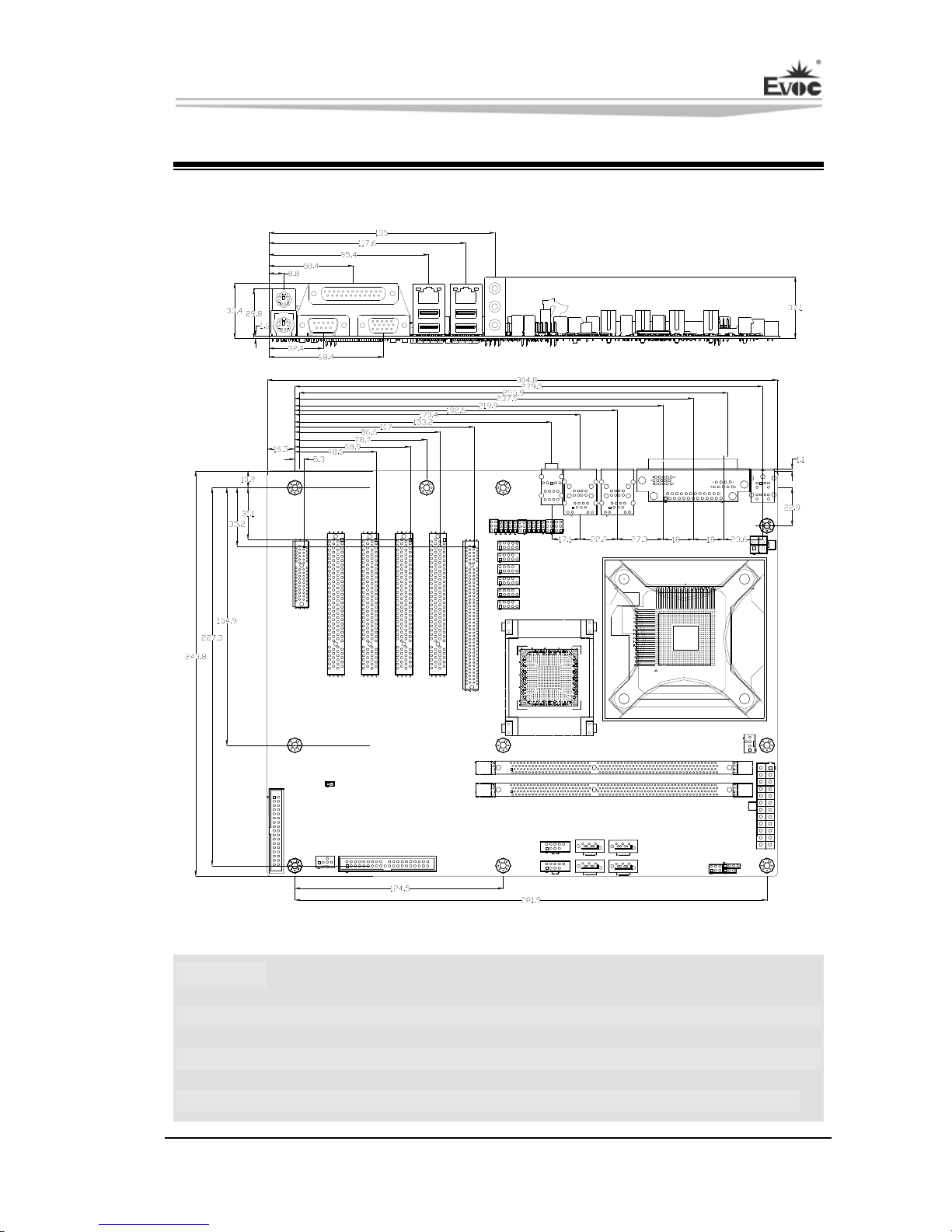
Product Outline
H1
H8 H2
H10
H6
H4
H5
H7
H9
H3
Unit: mm
Warning!
Please adopt appropriate screws and proper installation methods (including
board allocation, CPU and heat sink installation, etc); otherwise, the board may
be damaged. It is recommended to use M3x6 GB9074.4-88 screws at H1 ~ H10.
Page 11
Chapter 2 Installation
- 6 - EC0-1814(B)
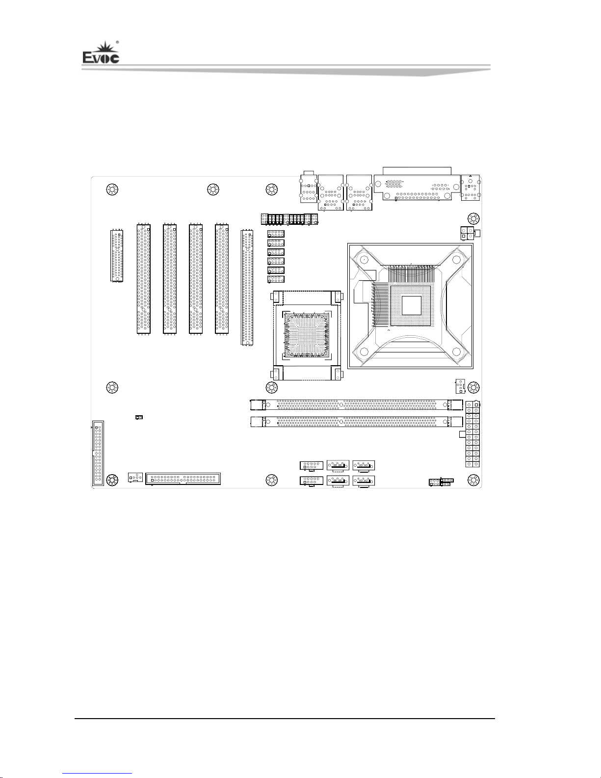
Locations of Connectors
H1
H8 H2
AUDIO1
J3
J2
J1
KM1
H10
PWR2
PCIE2
PCI1
PCI2
PCI3
PCI4
PCIE1
GPIO1
COM2
COM3
COM4
COM5
COM6
JP1
JP2
JP3
JP4
JP5
JP6
JP7
JP8
JP9
JP10
JP11
JP12
CPUFAN1
PWR1
H6
FP1
FP3
FP2
H4
J5
SATA1
SATA2
SATA3 SATA4
J4
H5
FDD1
H7
SYSFAN1
IDE1
DIMM1
DIMM2
H9
H3
JCC1
Page 12
Chapter 2 Installation
EC0-1814(B) - 7 -
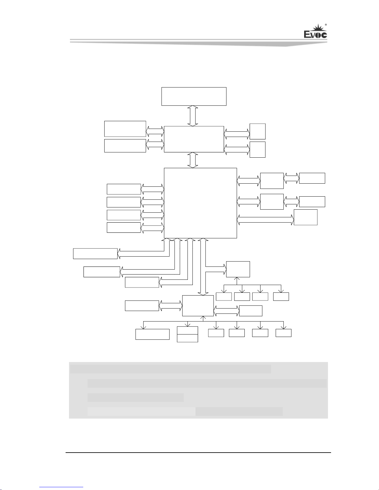
Structure
FDD
4*PCI SLOT
1*PCIe X4SLOT
1*PCIe X16SLOT
LPC TO
UART
IDE
COM3 COM4 COM5 COM6
PATA
PCIe
PC I BUS
Display Interface
Fa n Control
PCIe x4
ICH7R
Mouse
LGA775 Processor
Parallel
SATA
DDR3
SPI Flash
CH B
Hardwa re Moni tor
HDA Audi o
LAN2
RJ45
DIMM2
NH82801G R
LAN1
GMCH
LPC SIO
SATA Port 1~4
CH A
DMI X4
10/100/1000
Mbps LAN
USB 2.0
G41
Fan Control
VGA
MAX =24W
RJ45
DIMM1
MAX =3.3W
SPI
Keyboard
Conne ctor
Connector
PCI-E Port 6
DDR3
USB 2.0
COM2
HDA
COM1
PCI-E Port 5
LPC Bus
USB P ORT 4~7
USB P ORT 0~3
FSB
Bus
8GPIO
10/100/1000
Mbps LAN
Tip: How to identify the first pin of the jumpers and connectors
1. Observe the letter beside the socket: the first pin is usually marked with “1” or
bold lines or triangular symbols;
2. Observe the solder pad on the back; the square pad is the first pin.
Page 13
Chapter 2 Installation
- 8 - EC0-1814(B)
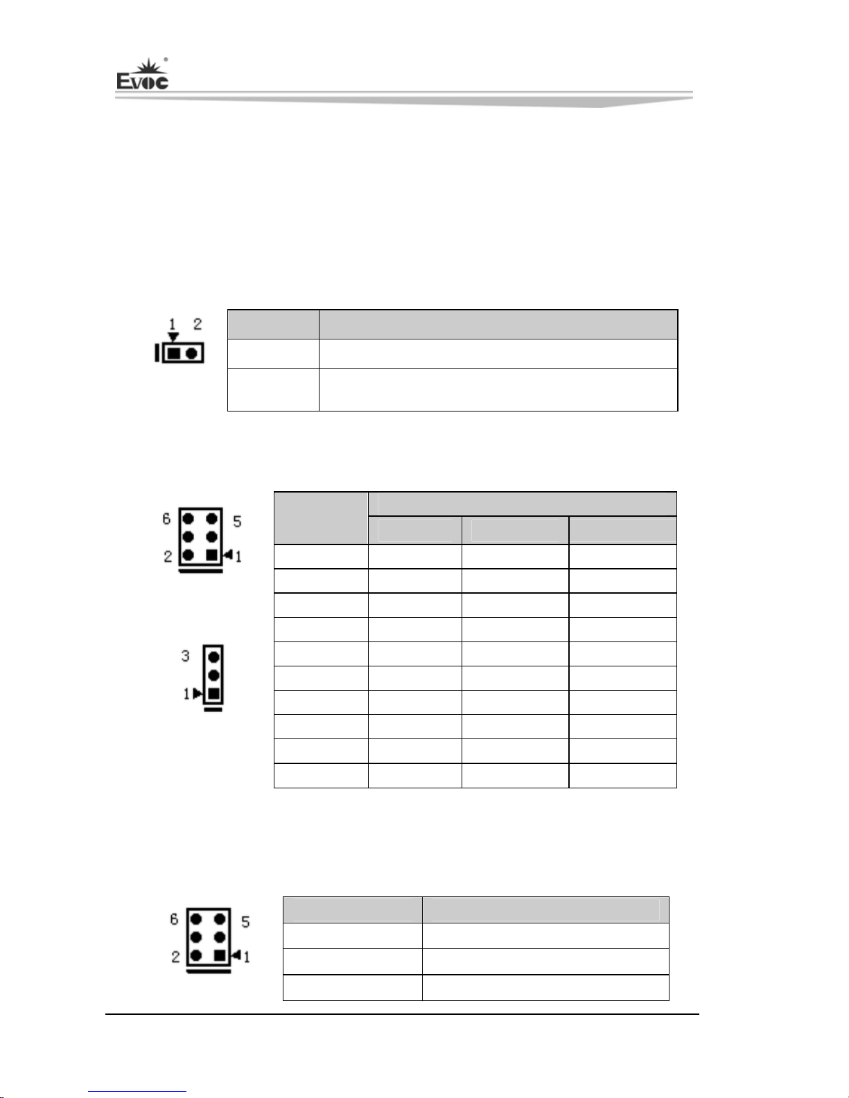
Jumper Setting
1. JCC1: Clear/Keep CMOS Setting (Pitch: 2.54mm)
CMOS is powered by the button battery on board. Clearing CMOS will restore
original settings (factory default). The steps are listed as follows: (1) Turn off the
computer and unplug the power cable; (2) Instantly short circuit JCC1; (3) Turn on
the computer; (4) Follow the prompt on screen to enter BIOS setup when booting the
computer, load optimized defaults; (5) Save and exit. Please set as follows:
Setup Function
1-2 Open Normal ((Default)
JCC1
1-2 Short
Clear the contents of CMOS and all BIOS settings
will restore to factory default values.
2. JP1 ~ JP10: RS-232/RS-422/RS-485 Mode Selection for COM1 and COM2
(Pitch: 2.54mm)
Mode Selection
Pin
Setting
RS-232 RS-485 RS-422
JP1 1-2 3-4 5-6
JP2 1-2 2-3 2-3
JP3 1-2 2-3 2-3
JP4 1-2 2-3 2-3
JP5 1-2 2-3 2-3
JP6 1-2 3-4 5-6
JP7 1-2 2-3 2-3
JP8 1-2 2-3 2-3
JP9 1-2 2-3 2-3
JP1/JP6
JP2 ~ JP5
JP7 ~ JP10
JP10 1-2 2-3 2-3
Note: JP1 ~ JP5 are used to set COM1; JP6 ~ JP10 are used to set COM2.
3. JP11 ~ JP12: Choose Voltage Mode for Serial Port with Power (Pitch:
2.54mm)
Setup Function
1-2 Short Normal ((Default)
3-4 Short Choose 5V Serial Port
JP11/JP12
5-6 Short Choose 12V Serial Port
Page 14
Chapter 2 Installation
EC0-1814(B) - 9 -
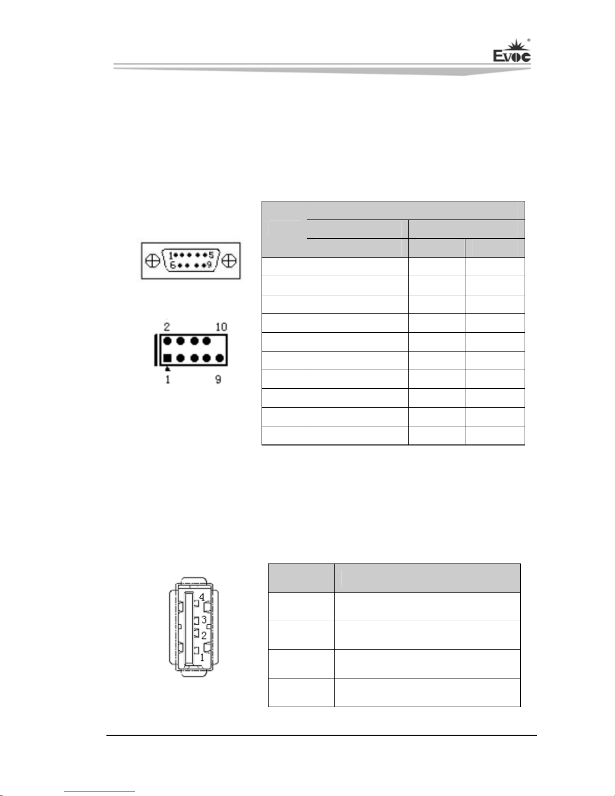
Serial Port
The board provides one standard DB9 serial port and five 2x5Pin serial port (Pitch:
2.54mm). COM1 and COM2 support RS-232/RS-422/RS-485 mode. The board
adopts VGA+PRINTER+COM combo socket and the model is 1262-049-401-910-N
of ETL and the model of the corresponding terminal is 1165-109-001-000 of ETL or
the D-SUB 9Pin female terminals of other manufacturers.
Signal Name
COM1 ~ COM6 COM1/COM2
Pin
RS-232 RS-422 RS-485
1 DCD# TXD- Data-
2 RXD TXD+ Data+
3 TXD RXD+ NC
4 DTR# RXD- NC
5 GND GND GND
6 DSR# NC NC
7 RTS# NC NC
8 CTS# NC NC
9 RI# NC NC
J1(COM1)
COM2 ~ COM6
10 NA NA NA
Note: the data transmission direction is controlled automatically at RS-485 mode.
USB Port
The board provides two sets of RJ45+dual USB connectors (J2 and J3) and two sets
of 2x5Pin USB pin headers (J4 and J5, Pitch: 2.54mm), which can support eight USB
devices in all.
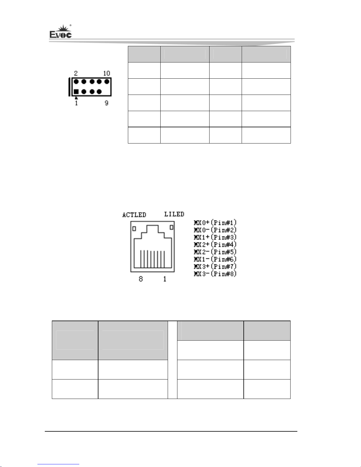
Pin Signal Name
1
+5V
2
USB_Data-
3
USB_Data+
J2/J3(USB)
4
GND
Note: it adopts RJ45+2USB combo socket of SUYIN 020180M500PM417ZA;
Page 15
Chapter 2 Installation
- 10 - EC0-1814(B)
Pin Signal Name Pin Signal Name
1
+5V 2 +5V
3
USB1_Data- 4 USB2_Data-
5
USB1_Data+ 6 USB2_Data+
7
GND 8 GND
J4/J5
9
NA 10 GND
LAN Port
The board provides two 10/100/1000Mbps LAN ports, RJ45+dual USB connectors
(J2 and J3).
J2/J3(LAN)
LILED
(Dual-Color: Y/G)
LAN Speed
Indicator
ACTLED
(Green)
LAN Activity
Status Indicator
Green 1000Mbps
Blink Data Transmitting Yellow 100Mbps
Off No Data to Transmit Off 10Mbps
Note: it adopts RJ45+2USB combo socket of SUYIN 020180M500PM417ZA.
Page 16
Chapter 2 Installation
EC0-1814(B) - 11 -
Power Connector
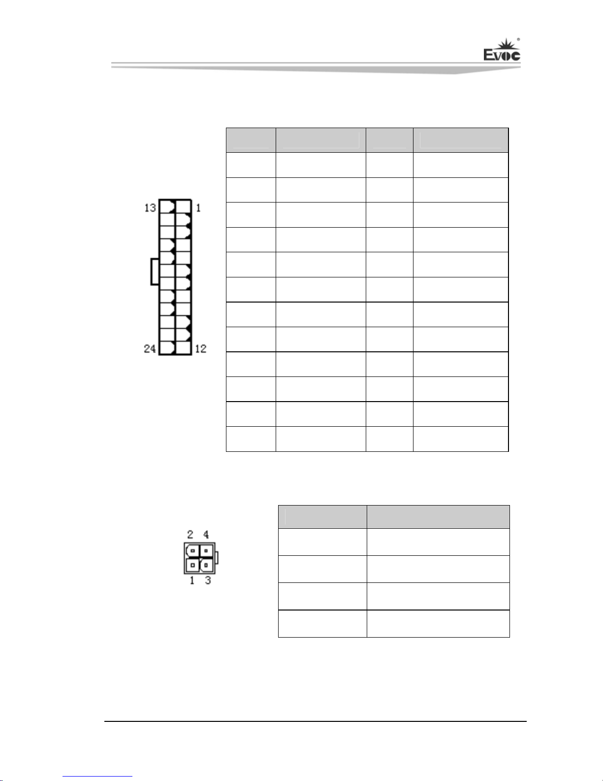
1. 24 Pin ATX Power Connector (Pitch: 4.2mm)
Pin Signal Name Pin Signal Name
1 +3.3V 13 +3.3V
2 +3.3V 14 -12V
3 GND 15 GND
4 +5V 16 PS_ON#
5 GND 17 GND
6 +5V 18 GND
7 GND 19 GND
8 PWROK 20 -5V
9 +5VSB 21 +5V
10 +12V 22 +5V
11 +12V 23 +5V
PWR1
12 +3.3V 24 GND
2. ATX 12V Power Connector (Pitch: 4.2mm)
Pin Signal Name
1 GND
2 GND
3 +12V
PWR2
4 +12V
Page 17
Chapter 2 Installation
- 12 - EC0-1814(B)
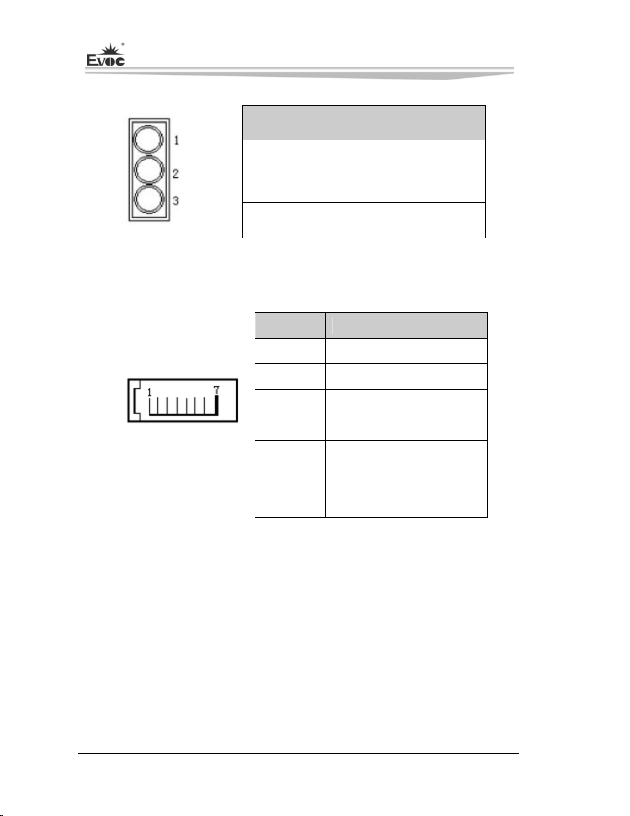
Audio Connector
Pin Signal Name
1 LINE_IN
2 LINE_OUT
AUDIO1
3 MIC_IN
SATA Connector
The board provides four standard SATA connectors, supporting RAID0, 1, 5 and 10.
Pin Signal Name
1 GND
2 TX+
3 TX-
4 GND
5 RX-
6 RX+
SATA1 ~ SATA4
7 GND
Hot-swap of SATA Hard Disk
Notes for hot-swap of SATA hard disk:
1. The hard disk shall support SATA 2.0 and use 15-pin SATA hard disk power
connector.
2. The driver of chipset shall support the hot-swap of SATA hard disk.
3. Hot-swap of SATA hard disk with the operating system is forbidden when system
is powered-on.
Page 18
Chapter 2 Installation
EC0-1814(B) - 13 -
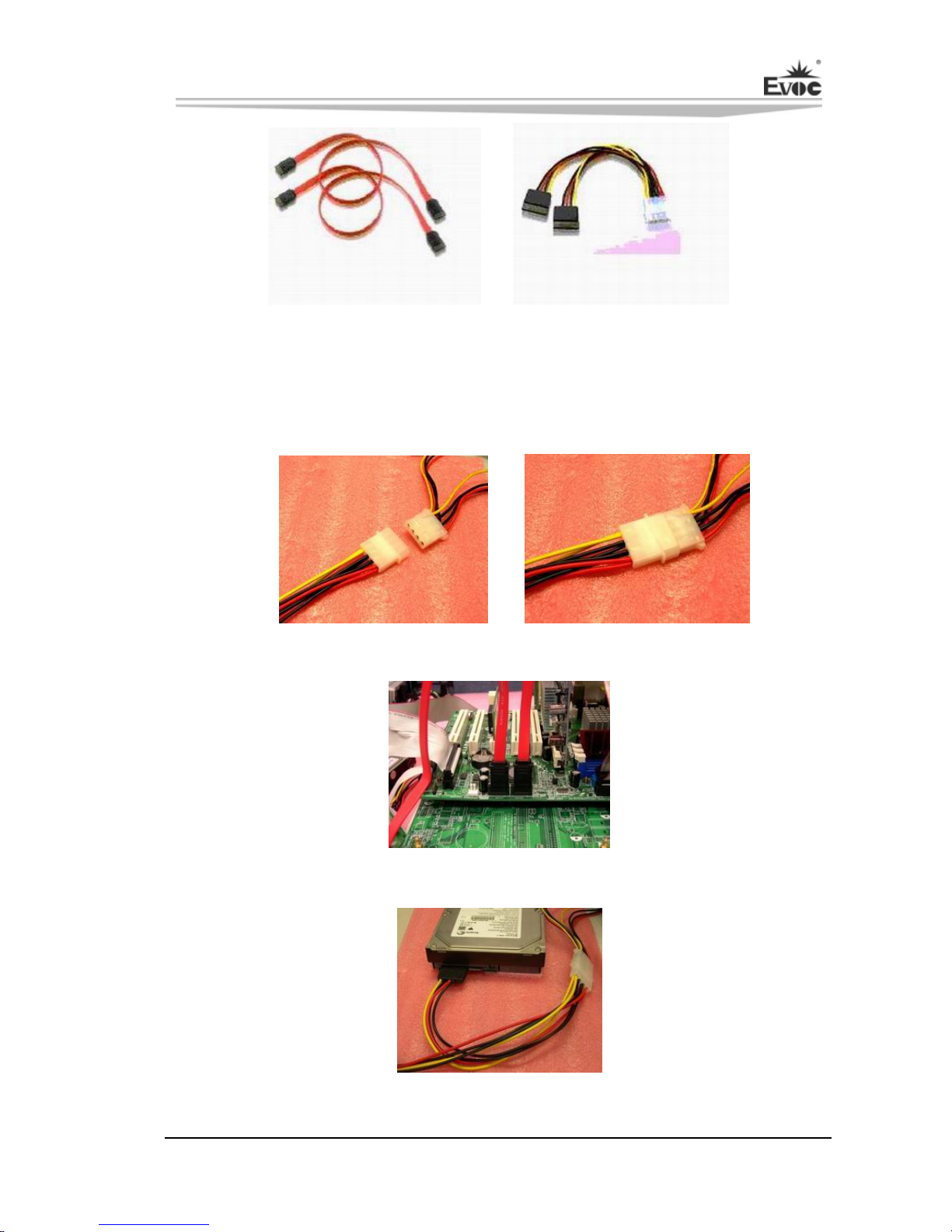
Please carry out hot plugging as follows. Improper operation may destroy the hard
disk or result in data loss.
Hot Plug
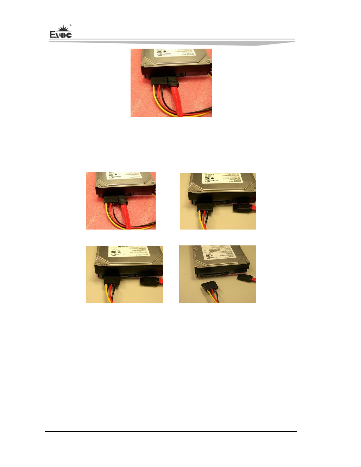
Step 1: Please plug the 1 x 4 pin SATA power connector (white) into the power adapter.
Step 2: Please connect the SATA data cable to the SATA connector on board.
Step 3: Please connect the 15-pin SATA power connector (black) to the SATA hard
disk.
SATA Data Cable SATA Power Cable
Page 19
Chapter 2 Installation
- 14 - EC0-1814(B)
Step 4: Please connect the SATA data cable to the SATA hard disk.
Hot Unplug
Step 1: Uninstall the hard disk from the device manager.
Step 2: Unplug the data cable from the SATA hard disk.
Step 3: Unplug the SATA 15-pin power connector (black) from the SATA hard disk.
Page 20
Chapter 2 Installation
EC0-1814(B) - 15 -
Keyboard and Mouse Connector
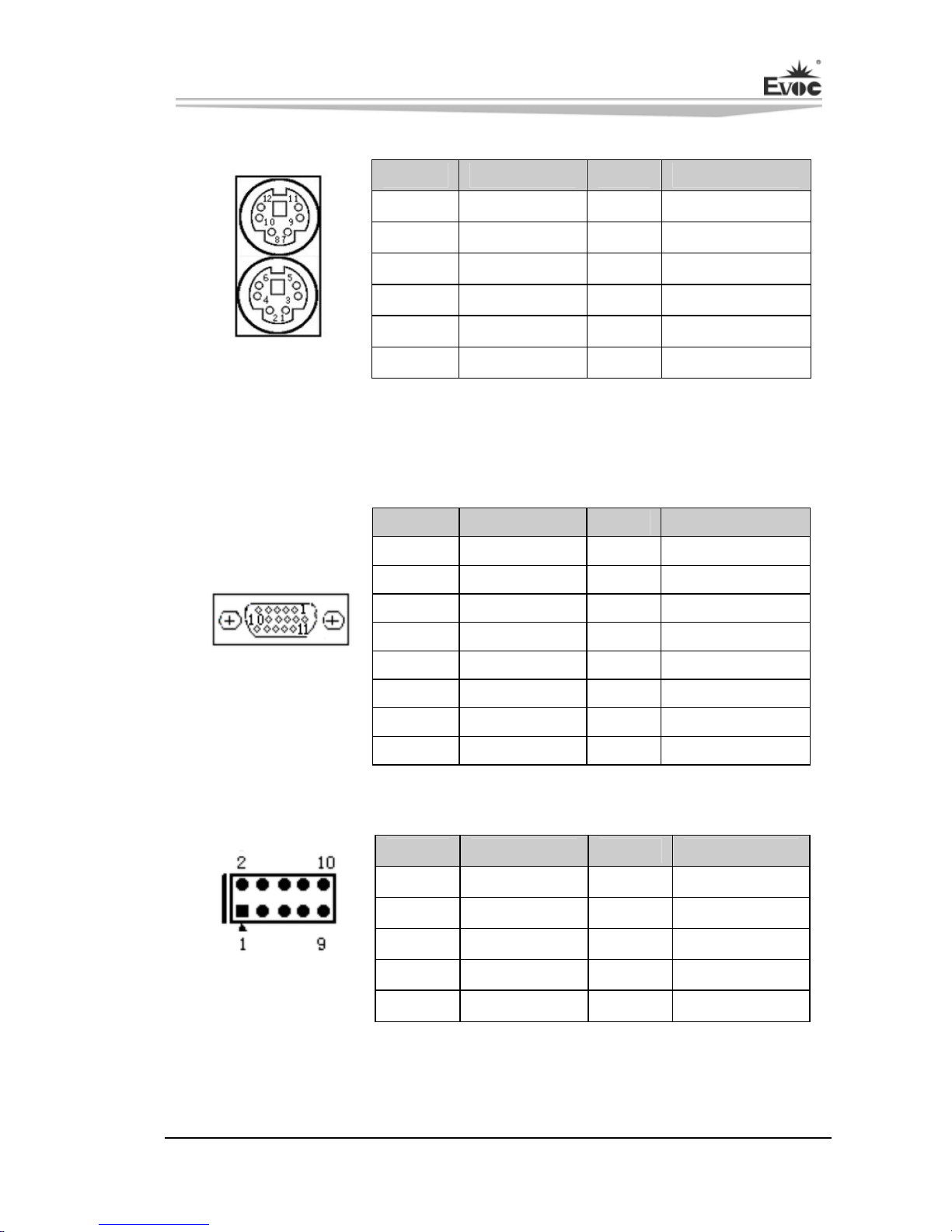
Pin Signal Name Pin Signal Name
1 KB_DATA 2 NC
3 GND 4 +5V
5 KB_CLK 6 NC
7 MS_DATA 8 NC
9 GND 10 +5V
KM1
11 MS_CLK 12 NC
VGA Graphic Connector
It adopts VGA+PRINTER+COM combo socket of ETL 1262-049-401-910-N; please
choose appropriate D-SUB 15Pin male terminal.
Pin Signal Name Pin Signal Name
1 Red 2 Green
3 Blue 4 NC
5 GND 6 GND
7 GND 8 GND
9 NC 10 GND
11 NC 12 DDCDATA
13 HSYNC 14 VSYNC
J1(VGA1
)
15 DDCCLK
GPIO Connector
Pin Signal Name Pin Signal Name
1 GPIO1 2 GPIO5
3 GPIO2 4 GPIO6
5 GPIO3 6 GPIO7
7 GPIO4 8 GPIO8
GPIO1
(Pitch: 2.54mm)
9 GND 10 NC
Note: the factory default values for the connector are pin 1, 3, 5 and 7 are for
TTL input while pin 2, 4, 6 and 8 are for TTL output. The voltage range for the
IO signals is 0 ~ 3.3V.
Page 21
Chapter 2 Installation
- 16 - EC0-1814(B)
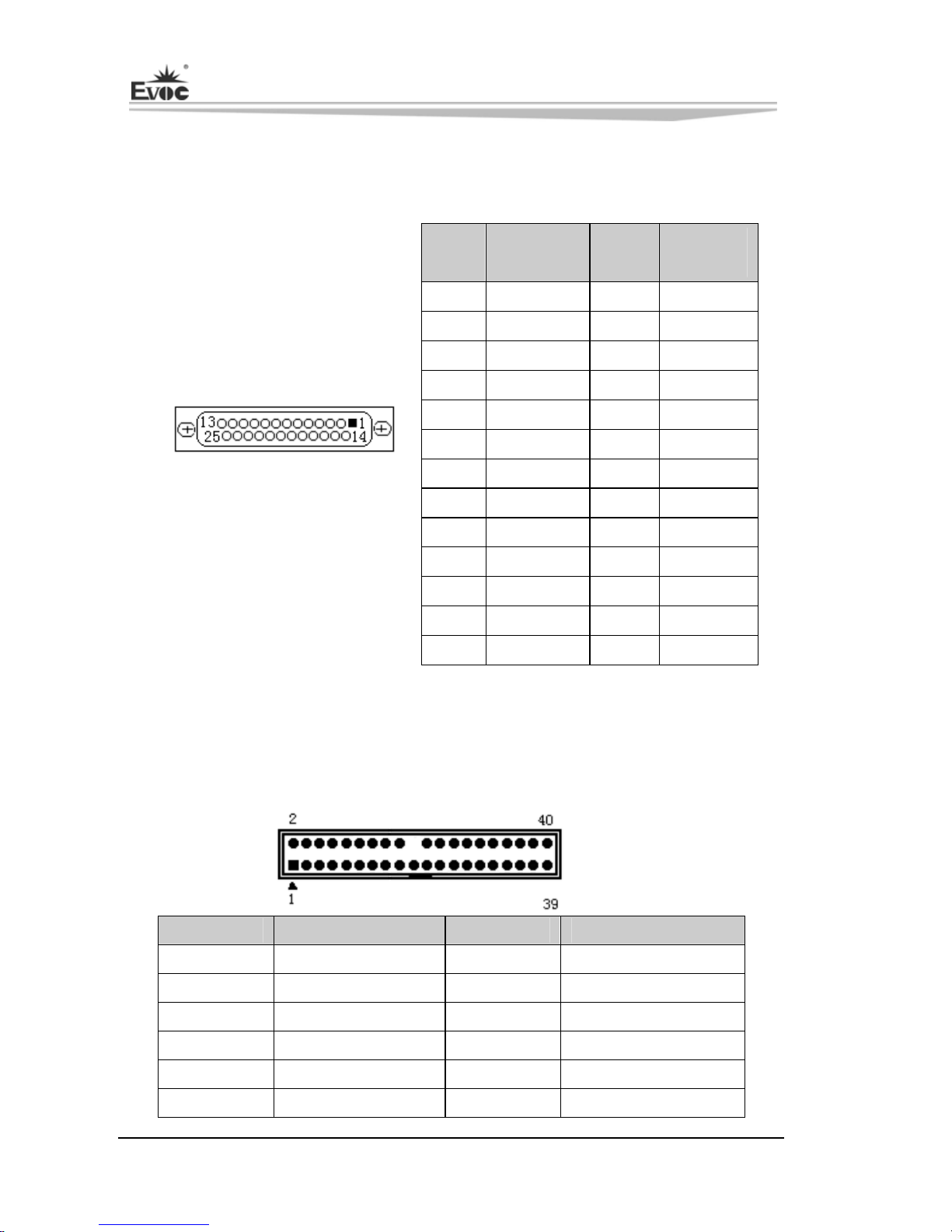
LPT Connector
It adopts VGA+PRINTER+COM combo socket of ETL 1262-049-401-910-N; please
choose appropriate D-SUB 25Pin male terminal.
Pin
Signal
Name
Pin
Signal
Name
1 STB# 14 AFD#
2 PD0 15 ERR#
3 PD1 16 INIT#
4 PD2 17 SLIN#
5 PD3 18 GND
6 PD4 19 GND
7 PD5 20 GND
8 PD6 21 GND
9 PD7 22 GND
10 ACK# 23 GND
11 BUSY 24 GND
12 PE 25 GND
J1(LPT)
13 SLCT
IDE Connector
The board provides one standard IDE connector (Pitch: 2.54mm), supporting Ultra
ATA/100/66/33, BMIDE and PIO modes.
IDE1
Pin Signal Name Pin Signal Name
1 RESET# 2 GND
3 D7 4 D8
5 D6 6 D9
7 D5 8 D10
9 D4 10 D11
11 D3 12 D12
Page 22
Chapter 2 Installation
EC0-1814(B) - 17 -
13 D2 14 D13
15 D1 16 D14
17 D0 18 D15
19 GND 20 KEY
21 DREQ 22 GND
23 IOW# 24 GND
25 IOR# 26 GND
27 IORDY 28 GND
29 DACK# 30 GND
31 IRQ 32 NC
33 DA1 34 ATA66_DET
35 DA0 36 DA2
37 CS1# 38 CS3#
39 LED# 40 GND
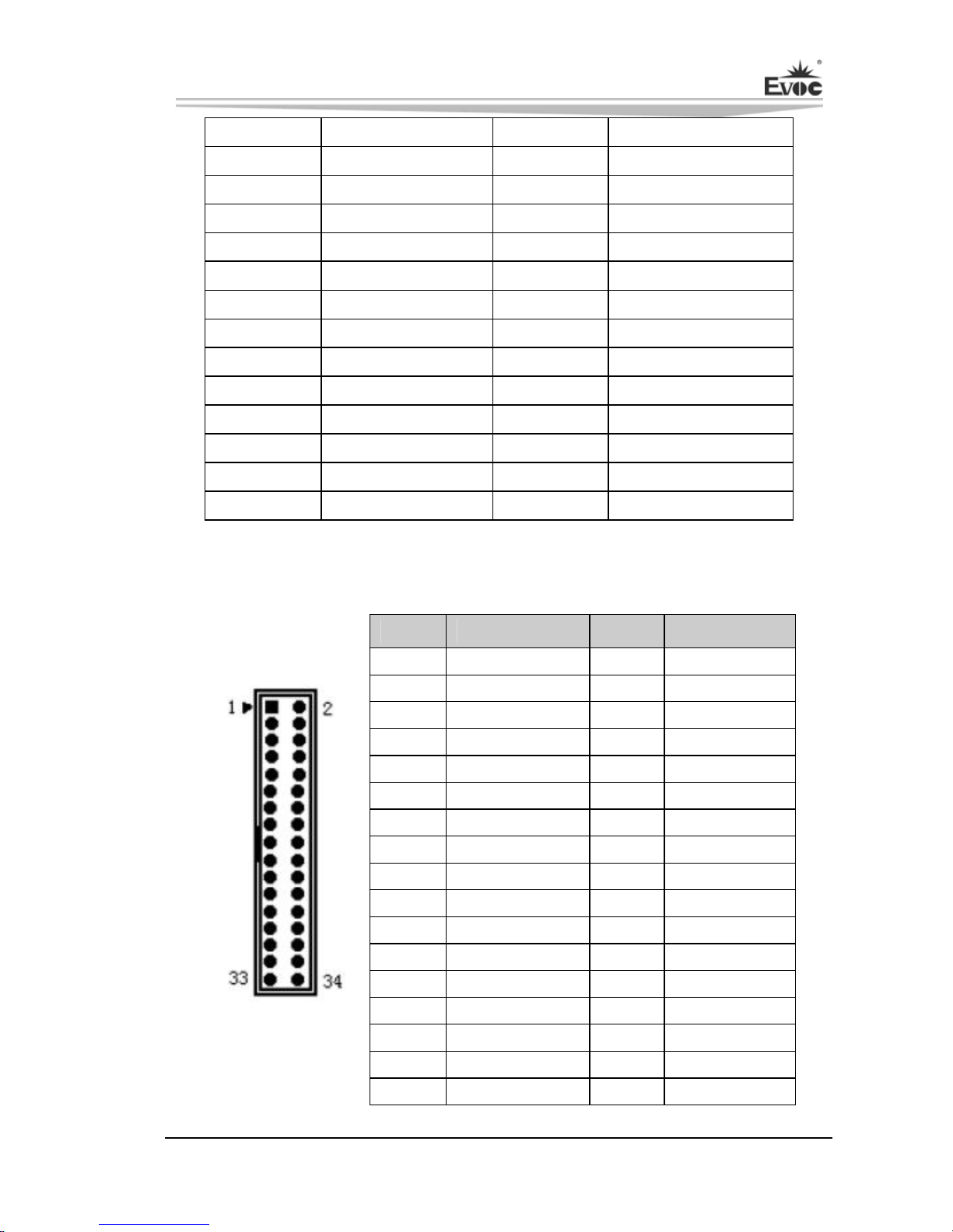
Floppy Driver Connector
The board provides one standard floppy driver connector (Pitch: 2.54mm).
Pin Signal Name Pin Signal Name
1 GND 2 DENSEL
3 GND 4 NC
5 KEY 6 DRATE
7 GND 8 INDEX#
9 GND 10 MOA#
11 GND 12 DSB#
13 GND 14 DSA#
15 GND 16 MOB#
17 GND 18 DIR#
19 GND 20 STEP#
21 GND 22 WD#
23 GND 24 WE#
25 GND 26 TRACKO#
27 GND 28 WP#
29 NC 30 RDATA#
31 GND 32 HDSEL#
FDD1
33 NC 34 DSKCHG#
Page 23
Chapter 2 Installation
- 18 - EC0-1814(B)
Status Indicator and Control Connector
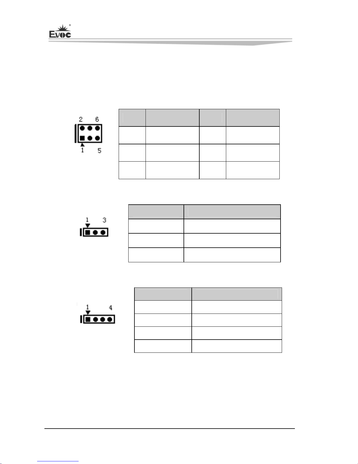
FP1, FP2 and FP3 are used to connect with the functional buttons or indicators
configured on the front panel of the chassis.
ATX Power Switch and HDD Indicator Connector (Pitch: 2.54mm)
Pin Signal Name Pin Signal Name
1 PWRBTN# 2 GND
3 GND 4 RESET#
FP1
5 HDD_LED- 6 HDD_LED+
Power Indicator Connector (Pitch: 2.54mm)
Pin Signal Name
1 +5V
2 NC
FP2
3 GND
Loudspeaker Output Connector (Pitch: 2.54mm)
Pin Signal Name
1 SPEAKER
2 NC
3 GND
FP3
4 +5V
Fan Connector
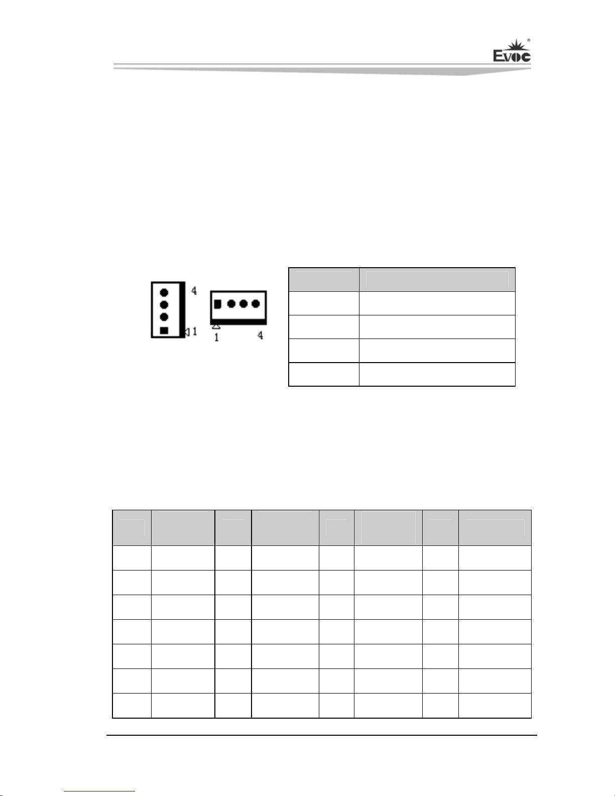
The board provides two standard fan connectors (CPUFAN1 and SYSFAN1) with
PWM speed adjustment and speed feedback function. Pay attention to the following
three issues when using the fan socket:
Page 24
Chapter 2 Installation
EC0-1814(B) - 19 -
The current for fan shall not exceed 700mA (12V);
Please confirm that the fan cable complies with the socket cable. Power cable
(usually red) is in the middle position. In addition, please confirm the earth
cable (usually black) and fan speed output impulse signal cable (other colors).
Some fans have no speed detection while the output of the cable is up to 12V, so
using these substandard connections will destroy the CPU card. It is
recommended to use a fan with speed detection.
Adjust the fan’s airflow to the direction of heat venting.
Pin Signal Name
1 GND
2 +12V
3 FAN_IO
CPUFAN1 SYSFAN1
(Pitch: 2.54mm)
4 FAN_PWM
Note: FAN_IO: fan speed impulse output; FAN_PWM: fan speed PWM control.
PCI Slot
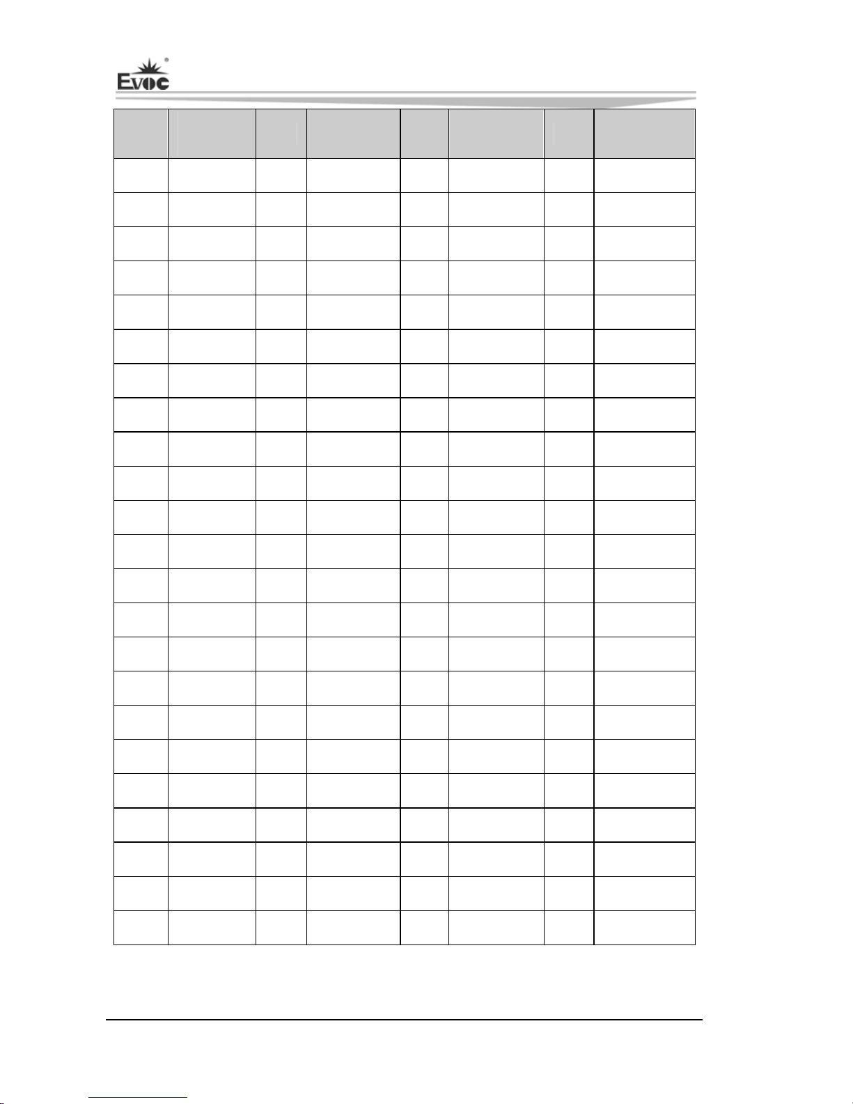
The board provides four standard PCI slots (PCI1/ PCI2 /PCI3 /PCI4);
SLOTS(version2.2) and 5V system Environment.
Pin
Signal
Name
Pin
Signal
Name
Pin
Signal
Name
Pin Signal Name
A1 TRST# A31 PCI_AD18 B1 -12V B31 +3.3V
A2 +12V A32 PCI_AD16 B2 TCK B32 PCI_AD17
A3 TMS A33 +3.3V B3 GND B33 PCI_C/BE#2
A4 TDI A34
PCI_FRAM
B4 TDO B34 GND
A5 +5V A35 GND B5 +5V B35 PCI_IRDY#
A6 INTA# A36 PCI_TRDY# B6 +5V B36 +3.3V
A7 INTC# A37 GND B7 INTB# B37
PCI_DEVSE
Page 25
Chapter 2 Installation
- 20 - EC0-1814(B)
Pin
Signal
Name
Pin
Signal
Name
Pin
Signal
Name
Pin Signal Name
A8 +5V A38 PCI_STOP# B8 INTD# B38 GND
A9 Null A39 +3.3V B9 PRSNT1# B39 PCI_PLOCK#
A10 +5V A40 NULL B10 Null B40 PCI_PERR#
A11 Null A41 NULL B11 PRSNT2# B41 +3.3V
A12 GND A42 GND B12 GND B42 PCI_SERR#
A13 GND A43 PCI_PAR B13 GND B43 +3.3V
A14 3.3Vaux A44 PCI_AD15 B14 Null B44 PCI_C/BE#1
A15 PCI_RST# A45 +3.3V B15 GND B45 PCI_AD14
A16 +5V A46 PCI_AD13 B16 PCI_CLK B46 GND
A17 PCI_GNT# A47 PCI_AD11 B17 GND B47 PCI_AD12
A18 GND A48 GND B18 PCI_REQ# B48 PCI_AD10
A19 PCI_PME# A49 PCI_AD9 B19 +5V B49 GND
A20 PCI_AD30 A50 PCI_C/BE#0 B20 PCI_AD31 B50 PCI_AD8
A21 +3.3V A51 +3.3V B21 PCI_AD29 B51 PCI_AD7
A22 PCI_AD28 A52 PCI_AD6 B22 GND B52 +3.3V
A23 PCI_AD26 A53 PCI_AD4 B23 PCI_AD27 B53 PCI_AD5
A24 GND A54 GND B24 PCI_AD25 B54 PCI_AD3
A25 PCI_AD24 A55 PCI_AD2 B25 +3.3V B55 GND
A26
PCI_IDSE
A56 PCI_AD0 B26 PCI_C/BE#3 B56 PCI_AD1
A27 +3.3V A57 +5V B27 PCI_AD23 B57 +5V
A28 PCI_AD22 A58
PCI_REQ64
B28 GND B58 PCI_ACK64#
A29 PCI_AD20 A59 +5V B29 PCI_AD21 B59 +5V
A30 GND A60 +5V B30 PCI_AD19 B60 +5V
Page 26
Chapter 2 Installation
EC0-1814(B) - 21 -
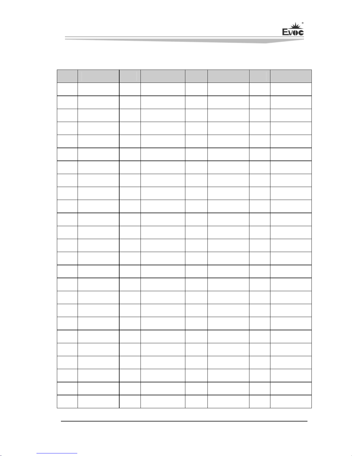
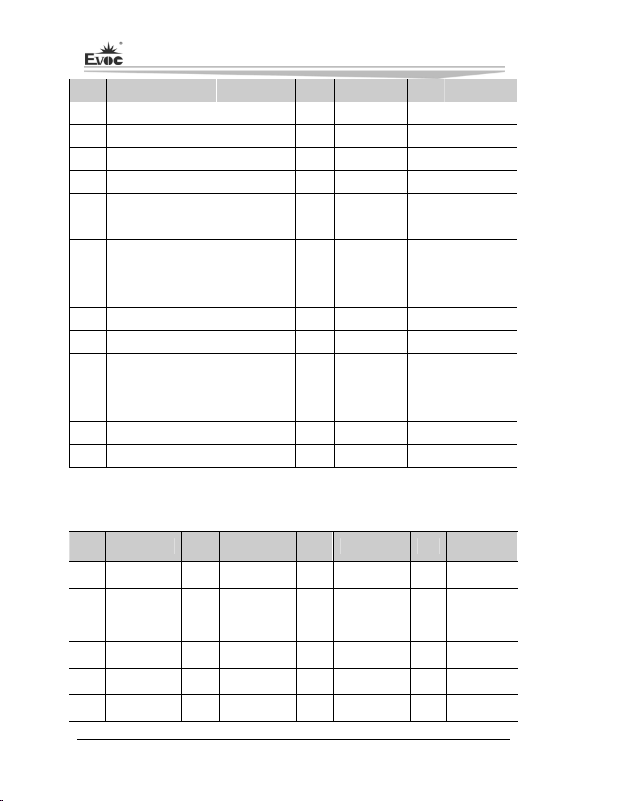
PCIex16 Slot
Marked as PCIE1 on-board.
Pin Signal Name Pin Signal Name Pin Signal Name Pin Signal Name
A1 PRSNT1# A2 +12V B1 +12V B2 +12V
A3 +12V A4 GND B3 RSVD B4 GND
A5 TCK A6 TDI B5 SMCLK B6 SMDATA
A7 TDO A8 TMS B7 GND B8 +3.3V
A9 +3.3V A10 +3.3V B9 TRST# B10 3.3Vaux
A11 PWRGD A12 GND B11 WAKE# B12 RSVD
A13 REFCLK+ A14 REFCLK- B13 GND B14 PETp0
A15 GND A16 PERp0 B15 PETn0 B16 GND
A17 PERn0 A18 GND B17 PRSNT2# B18 GND
A19 RSVD A20 GND B19 PETp1 B20 PETn1
A21 PERp1 A22 PERn1 B21 GND B22 GND
A23 GND A24 GND B23 PETp2 B24 PETn2
A25 PERp2 A26 PERn2 B25 GND B26 GND
A27 GND A28 GND B27 PETp3 B28 PETn3
A29 PERp3 A30 PERn3 B29 GND B30 RSVD
A31 GND A32 RSVD B31 PRSNT2#A B32 GND
A33 RSVD A34 GND B33 PETp4 B34 PETn4
A35 PERp4 A36 PERn4 B35 GND B36 GND
A37 GND A38 GND B37 PETp5 B38 PETn5
A39 PERp5 A40 PERn5 B39 GND B40 GND
A41 GND A42 GND B41 PETp6 B42 PETn6
A43 PERp6 A44 PERn6 B43 GND B44 GND
A45 GND A46 GND B45 PETp7 B46 PETn7
A47 PERp7 A48 PERn7 B47 GND B48 PRSNT2#B
A49 GND A50 RSVD B49 GND B50 PETp8
Page 27
Chapter 2 Installation
- 22 - EC0-1814(B)
Pin Signal Name Pin Signal Name Pin Signal Name Pin Signal Name
A51 GND A52 PERp8 B51 PETn8 B52 GND
A53 PERn8 A54 GND B53 GND B54 PETp9
A55 GND A56 PERp9 B55 PETn9 B56 GND
A57 PERn9 A58 GND B57 GND B58 PETp10
A59 GND A60 PERp10 B59 PETn10 B60 GND
A61 PERn10 A62 GND B61 GND B62 PETp11
A63 GND A64 PERp11 B63 PETn11 B64 GND
A65 PERn11 A66 GND B65 GND B66 PETp12
A67 GND A68 PERp12 B67 PETn12 B68 GND
A69 PERn12 A70 GND B69 GND B70 PETp13
A71 GND A72 PERp13 B71 PETn13 B72 GND
A73 PERn13 A74 GND B73 GND B74 PETp14
A75 GND A76 PERp14 B75 PETn14 B76 GND
A77 PERn14 A78 GND B77 GND B78 PETp15
A79 GND A80 PERp15 B79 PETn15 B80 GND
A81 PERn15 A82 GND B81 PRSNT2#C B82 RSVD
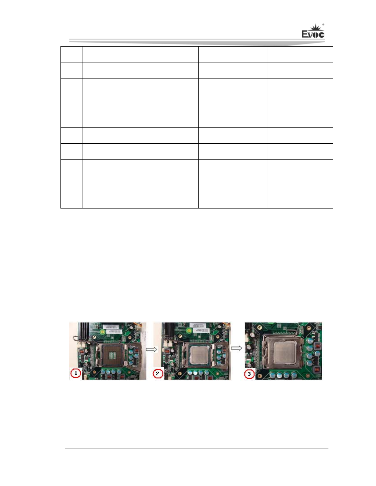
PCIex4 Slot
Marked as PCIE2 on-board.
Pin Signal Name Pin Signal Name Pin Signal Name Pin Signal Name
A1 PRSNT1# A2 +12V B1 +12V B2 +12V
A3 +12V A4 GND B3 RSVD B4 GND
A5 TCK A6 TDI B5 SMCLK B6 SMDATA
A7 TDO A8 TMS B7 GND B8 +3.3V
A9 +3.3V A10 +3.3V B9 TRST# B10 3.3Vaux
A11 PWRGD A12 GND B11 WAKE# B12 RSVD
Page 28
Chapter 2 Installation
EC0-1814(B) - 23 -
A13 REFCLK+ A14 REFCLK- B13 GND B14 PETp0
A15 GND A16 PERp0 B15 PETn0 B16 GND
A17 PERn0 A18 GND B17 PRSNT2# B18 GND
A19 RSVD A20 GND B19 PETp1 B20 PETn1
A21 PERp1 A22 PERn1 B21 GND B22 GND
A23 GND A24 GND B23 PETp2 B24 PETn2
A25 PERp2 A26 PERn2 B25 GND B26 GND
A27 GND A28 GND B27 PETp3 B28 PETn3
A29 PERp3 A30 PERn3 B29 GND B30 RSVD
A31 GND A32 RSVD B31 PRSNT2#A B32 GND
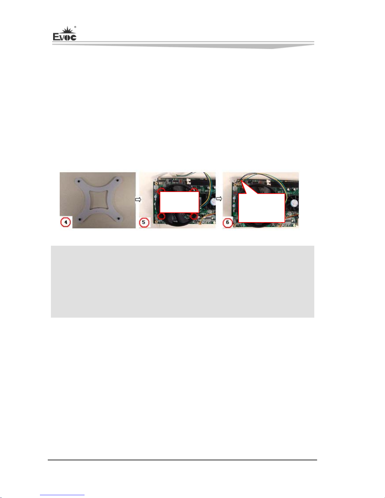
Install the CPU
Please install the CPU as follows (refer to the figure below):
Align the notches in the CPU with the notches on the socket and put the CPU
into the socket.
When the CPU is fully seated in the socket, close the upper cover on CPU
socket and then lock the CPU via hook.
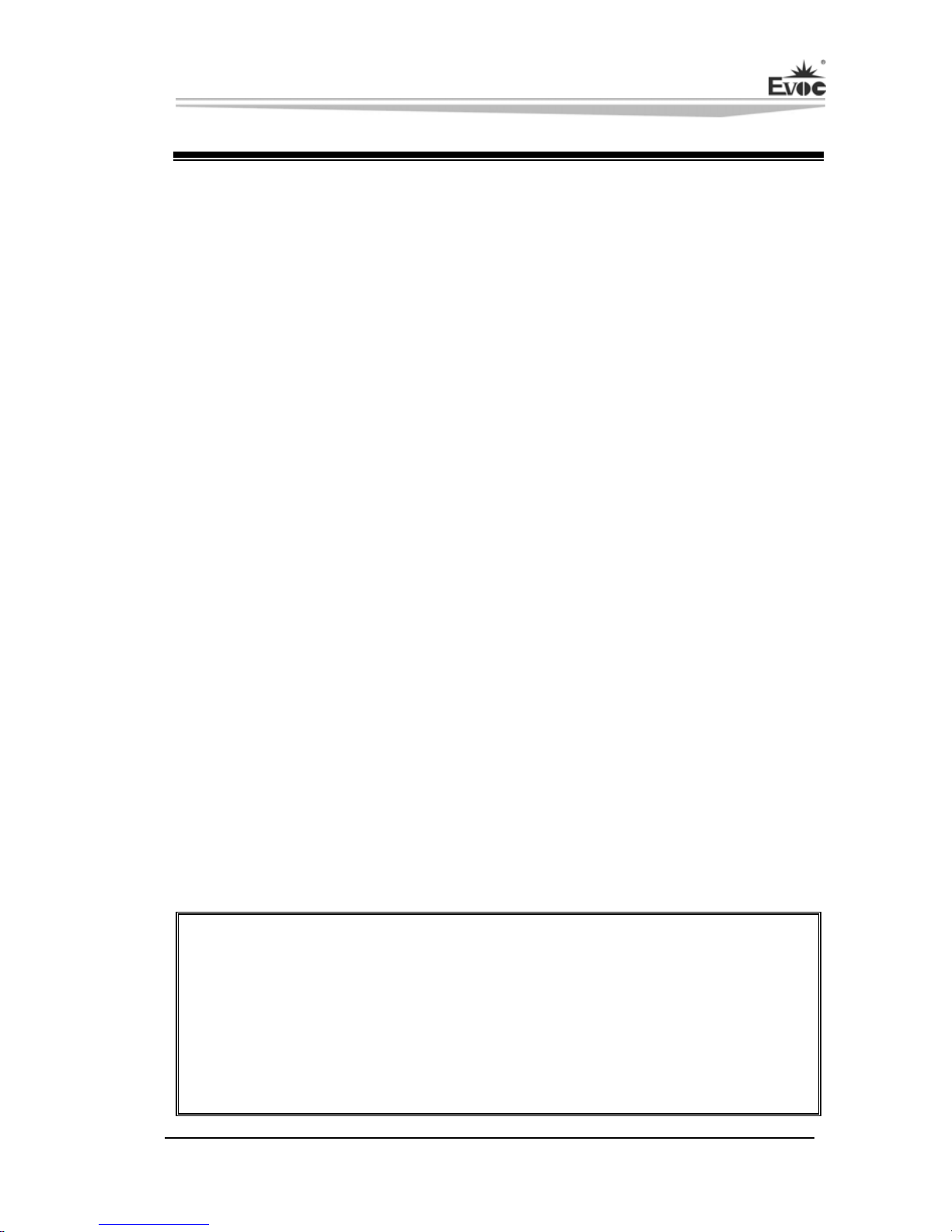
Install the CPU Fan
Please install the CPU fan as follows: (refer to the figure below):
Assemble the bracket of the cooling fin (refer to ④) with the fixing holes on the
Page 29
Chapter 2 Installation
- 24 - EC0-1814(B)
rear of the motherboard;
Connect the front side of cooling fin with the bracket and fix them (refer to ⑤);
take care that the surface between the cooling fin and the CPU crystal wafer
shall b
e well contacted;
Fix the cooling fin with two screws on the cross (do not tighten it) and then the
other two screws; then tighten the four screws;
Finally, connect the fan power cable to the fan socket on the CPU card.
Note! It is recommended to use cooling fan authenticated by Intel; before installing
the fan, smear the heat sink compound on the surface between CPU and the fan
cooling fin to improve the heat dissipation performance; always check whether the fan
is operating normally to ensure the heat dissipation within the chassis. When holding a
board, please hold the edge instead of the cooling fin.
Tighten the
screws on
CPU radiato
r
.
Connect the CPU
fan plug with the
relevant
Page 30
Chapter 3 BIOS Setup
EC0-1814(B) - 25 -
Chapter 3 BIOS Setup
BIOS Overview
BIOS (Basic Input and Output System) is solidified in the flash memory on the CPU
board. Its main functions include: initialize system hardware, set the operating status
of the system components, adjust the operating parameters of the system components,
diagnose the functions of the system components and report failures, provide hardware
operating and controlling interface for the upper level software system, guide
operating system and so on. BIOS provides users with a human-computer interface in
menu style to facilitate the configuration of system parameters for users, control power
management mode and adjust the resource distribution of system device, etc.
Correct BIOS settings make system more stable and reliable and also improve the
overall performance of the system. Inappropriate or wrong BIOS settings reduce the
performance of system, make system unstable and even unable to work normally.
BIOS Parameter Setup
Prompt message for BIOS setting may appear once the system is powered on and the
computer booted. At that time (invalid at other time), press the key specified in the
prompt message (usually <Del>) to enter into BIOS setting.
If the BIOS setting in CMOS is destroyed, system will ask you to enter BIOS setting
or select certain default value.
All the setup values modified by BIOS are saved in the CMOS storage of the system.
The CMOS storage is powered by battery; unless clearing CMOS is executed, the
settings would not be lost even when the power supply is cut off.
Note! BIOS setting will influence the computer performance directly. Wrong
settings may damage computer or even prevent boot up. After clearing CMOS, use
the internal default value of BIOS to restore the normal operation of system.
Our company is constantly researching and updating BIOS, so the setup interface
may be a bit different. The figure below is for reference only; it may be different
from your BIOS setting procedure in use.
Page 31
Chapter 3 BIOS Setup
- 26 - EC0-1814(B)
Basic Function Setting for BIOS
After starting SETUP program, the main interface of CMOS Setup Utility will
appear:
BIOS SETUP UTILITY
System Overview
Processor
Type :
Genuine Intel(R) CPU @ 2.40GHz
Speed :2400MHz
Cores :2
System Memory
Size: 504MB
System Time [00:47:55]
System Date [Wed 01/02/2002]
←→ Select Screen
↑↓ Select Item
+ - Change Field
Tab Select Field
F1 General Help
F10 Save and Exit
ESC Exit
V02.57 (c)Copyright 1985-2004,American Megatrends, Inc.
Main
System Time
Choose this option and set the current time by < + > / < - >, which is
displayed in the format of hour/minute/second. Reasonable range for each
option is: Hour (00-23), Minute (00-59), Second (00-59).
System Date
Choose this option and set the current date by < + > / < - >, which is
displayed in the format of month/date/year. Reasonable range for each option
is: Month (Jan.-Dec.), Date (01-31), Year (Maximum to 2099), Week (Mon.
~ Sun.).
Page 32
Chapter 3 BIOS Setup
EC0-1814(B) - 27 -
Advanced
BIOS SETUP UTILITY
Advanced Settings
WARNING: Setting wrong values in below
sections may cause system to malfunction
CPU Configuration
IDE Configuration
Super IO Configuration
Hardware Health Configuration
USB Configuration
Power Management Configuration
Clock Generator Configuration
Configure CPU
←→ Select Screen
↑↓ Select Item
Enter Go to Sub Screen
Tab Select Field
F1 General Help
F10 Save and Exit
ESC Exit
V02.57 (c)Copyright 1985-2004, American Megatrends, Inc.
CPU Configuration
BIOS SETUP UTILITY
Configure advanced CPU settings
Module Version: 3F.1C
Manufacturer: Intel
Genuine Intel(R) CPU @ 2.40GHz
Frequency; :2.40GHz
FSB Speed; :800MHz
Cache L1; :32 KB
Cache L2; :512 KB
Core Multi-Processing [Enabled]
←→ Select Screen
↑↓ Select Item
+ - Change Field
Tab Select Field
F1 General Help
F10 Save and Exit
ESC Exit
V02.57 (c)Copyright 1985-2004, American Megatrends, Inc
Core Multi-Processing
Switch to enable CPU multi-core processing.
Page 33
Chapter 3 BIOS Setup
- 28 - EC0-1814(B)
IDE Configuration
BIOS SETUP UTILITY
IDE Configuration
ATA/IDE Configuration [Enhanced]
Configure SATA as [IDE]
Port0 SATA AHCI Speed Gen 2 (3.0 Gb/sec)
Primary IDE Master
:[Not Detected]
Primary IDE Slave
:[Not Detected]
Secondary IDE Master
:[Not Detected]
Secondary IDE Slave
:[Not Detected]
Third IDE Master
:[Not Detected]
Third IDE Slave
:[Not Detected]
Fourth IDE Master
:[Not Detected]
Fourth IDE Slave
:[Not Detected]
←→ Select Screen
↑↓ Select Item
+ - Change Field
Tab Select Field
F1 General Help
F10 Save and Exit
ESC Exit
V02.57 (c)Copyright 1985-2004, American Megatrends, Inc.
ATA/IDE Configuration
Mode selection for SATA#1 controller; there are three options: Disabled,
Compatible and Enhanced.
Configure SATA as
SATA controller type selection; there are three options for this item: IDE,
RAID and AHCI. Only when ATA/IDE Configuration is under Enhanced
mode, are RAID and AHCI supported.
Both RAID and AHCI functions require supports from hardware chip and
OS.
Primary ~ Fourth IDE Master/Slave
﹡Type
Not Installed: no IDE device can be detected by system;
AUTO: automatic detection of IDE parameters when powering on;
CD/DVD: used for ATAPI CDROM;
ARMD: used for various analog IDE devices.
﹡LBA/Large Mode
Used to set whether to support LBA mode or not.
Page 34
Chapter 3 BIOS Setup
EC0-1814(B) - 29 -
﹡Block(Multi-sector Transfer)
Used to set whether to support multi-sector simultaneous transfer or not.
﹡PIO Mode
Used for PIO mode setting.
﹡DMA Mode
Used for DMA mode setting.
﹡S.M.A.R.T
Used to set whether to enable S.M.A.R.T function and it is only effective for
the hard disk supporting this function.
﹡32Bit Data Transfer
This option is used to enable 32-bit hard disk accessing mode, which could
optimize hard disk read and write speed.
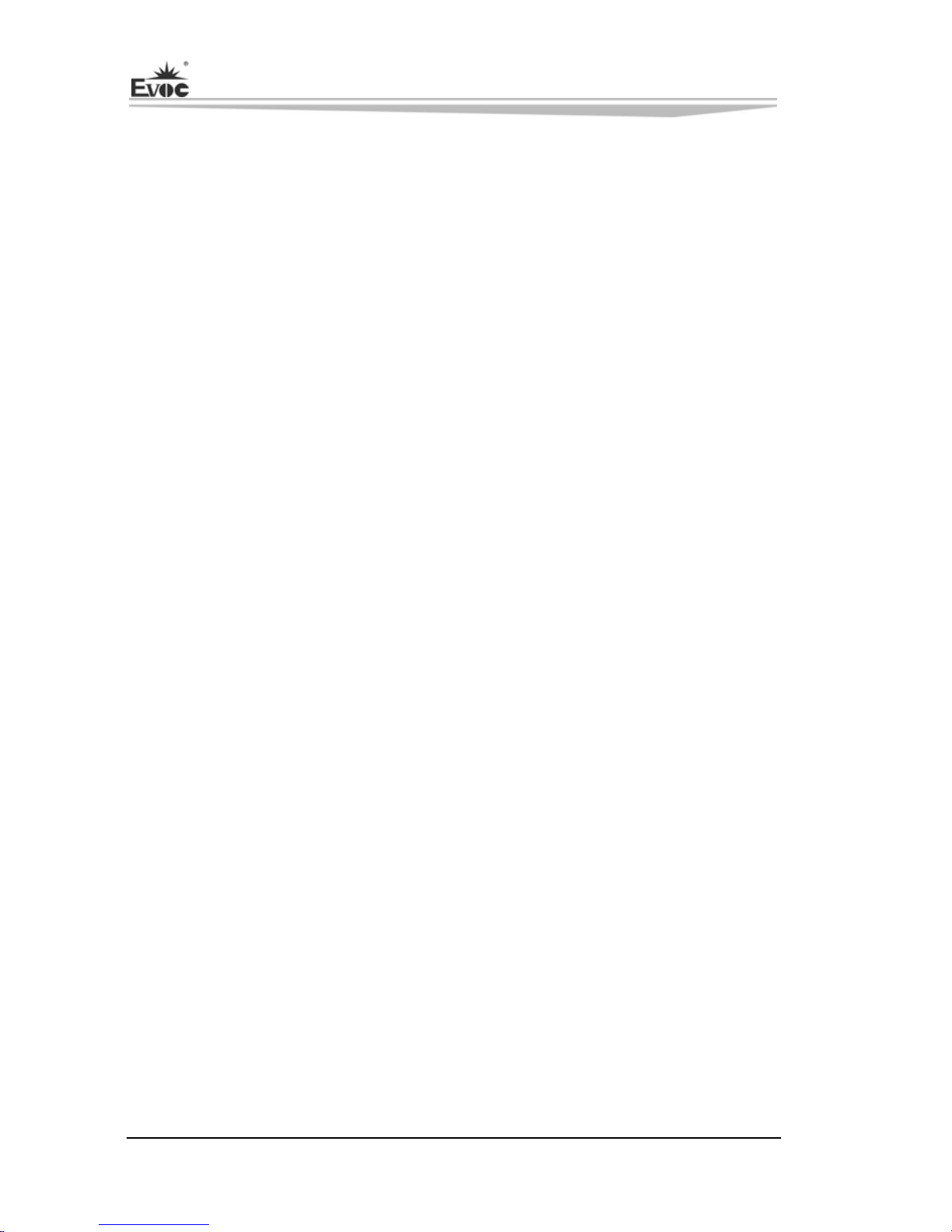
Super IO Configuration
BIOS SETUP UTILITY
Configure Super IO Chipset
Floppy A [1.44MB 31/2"]
OnBoard Floppy Controller [Enabled]
Serial Port1 Address [3F8/IRQ4]
Serial Port2 Address [2F8/IRQ3]
Uart IRQ Attribute [Level Active Low]
Serial Port3 Address [200]
Serial Port3 IRQ [10]
Serial Port4 Address [208]
Serial Port4 IRQ [10]
Serial Port5 Address [210]
Serial Port5 IRQ [10]
Serial Port6 Address [210]
Serial Port6 IRQ [10]
Parallel Port Address [378]
Parallel Port Mode [Normal]
Parallel Port IRQ [IRQ7]
Allows BIOS to Enable or
Disable Floppy
Controller.
←→ Select Screen
↑↓ Select Item
+ - Change Field
Tab Select Field
F1 General Help
F10 Save and Exit
ESC Exit
V02.57 (c)Copyright 1985-2004, American Megatrends, Inc.
Page 35
Chapter 3 BIOS Setup
- 30 - EC0-1814(B)
Floppy A
Configure the floppy driver type.
OnBoard Floppy Controller
Used to enable floppy controller.
Serial Port 1 Address
Set the addresses and IRQs of COM1 on motherboard. The options are:
Disabled, 3F8H/IRQ4, 3E8/IRQ4, 2E8/IRQ3 and 2F8H/IRQ3.
Serial Port 2 Address
Set the addresses and IRQs of COM2 on motherboard. The options are:
Disabled, 3F8H/IRQ4, 3E8/IRQ4, 2E8/IRQ3 and 2F8H/IRQ3.
Uart IRQ Attribute
Level Active Low: IRQ mode option under Windows system.
Edge Active High: IRQ mode option under Linux system.
Serial Port 3-6 Address
Set the addresses of COM3-6 on motherboard;
Serial Port 3-6 IRQ
Set the IRQs of COM3-6 on motherboard;
Parallel Port Address
Set the address of the parallel port on motherboard.
Parallel Port Mode
Set the mode for the parallel port on motherboard.
Parallel Port IRQ
Set the IRQ of the parallel port on motherboard.
Page 36
Chapter 3 BIOS Setup
EC0-1814(B) - 31 -
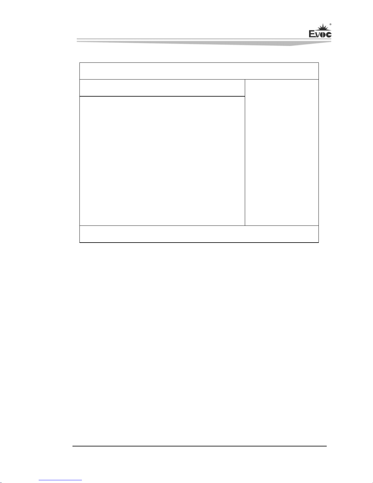
Hardware Health Configuration
BIOS SETUP UTILITY
Hardware Health Configuration
System Temperature : 34°C/93°F
CPU Temperature : 34°C/93°F
CPUFAN1 : 1577 RPM
SYSFAN1 : N/A
Vcore : 1.320 V
V3.3 : 3.312 V
V5.0 : 5.107 V
V12.0 : 11.481V
VBAT : 3.200 V
Enables Hardware
Health Monitoring
Device
←→ Select Screen
↑↓ Select Item
+ - Change Field
Tab Select Field
F1 General Help
F10 Save and Exit
ESC Exit
V02.57 (c)Copyright 1985-2004, American Megatrends, Inc.
System Temperature
Current system temperature, it is monitored by thermal resistor on
motherboard.
CPU Temperature
Current CPU temperature, it is monitored by temperature sensor on
motherboard.
CPUFAN1
Display the current CPU fan speed.
SYSFAN1
Display the current system fan speed.
Vcore
CPU core voltage;
V3.3/ V5.0/V12.0
Turn on/off power to output voltage;
Page 37
Chapter 3 BIOS Setup
- 32 - EC0-1814(B)
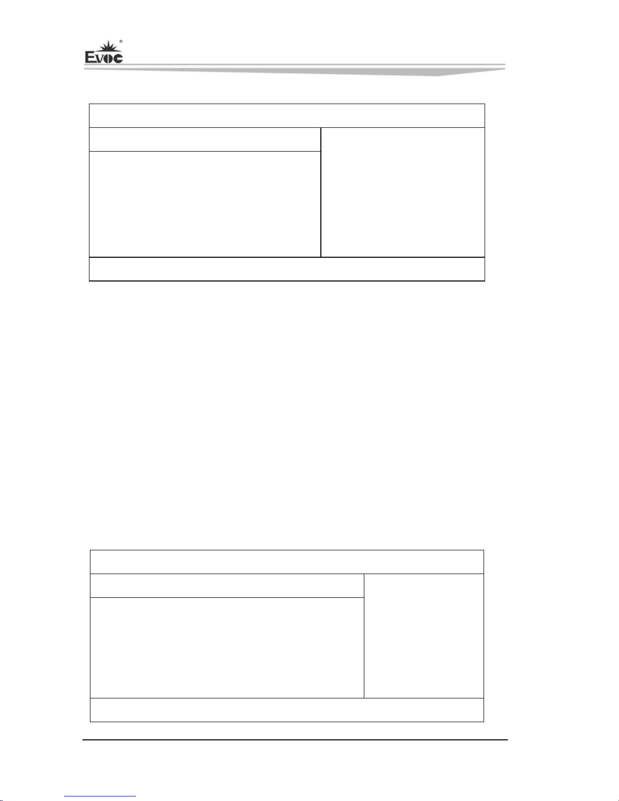
USB Configuration
BIOS SETUP UTILITY
USB Configuration
Module Version -2.24.0-12.4
USB Devices Enabled :
None
USB Function [8 USB Ports]
USB 2.0 Controller [Enabled]
Legacy USB Support [Auto]
Enables USB host controllers.
←→ Select Screen
↑↓ Select Item
+ - Change Field
F1 General Help
F10 Save and Exit
ESC Exit
V02.57 (c)Copyright 1985-2004, American Megatrends, Inc.
USB Function
This option is used to set the number of the USB controllers, i.e., to confirm
how many USB controllers are supported. One controller usually has two
USB connectors.
USB 2.0 Controller
This option is used to set whether to support USB 2.0 controller.
Legacy USB Support
This option is used to support legacy USB devices (keyboard, mouse and
storage device, etc.); when this option is set to Enabled, the USB device
could be used even if under OS that doesn’t support USB, such as DOS.
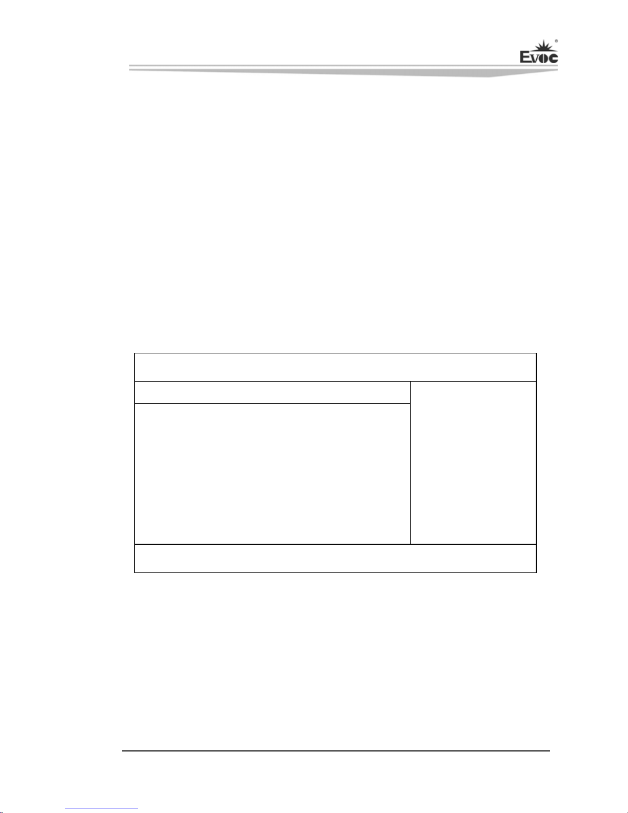
Power Management Configuration
BIOS SETUP UTILITY
Power Management Configuration
ACPI APIC Support [Enabled]
Restore on AC Power Loss [Last state]
Resume on RTC Alarm [Disabled]
←→ Select Screen
↑↓ Select Item
+ - Change Field
F1 General Help
F10 Save and Exit
ESC Exit
V02.57 (c)Copyright 1985-2004, American Megatrends, Inc.
Page 38
Chapter 3 BIOS Setup
EC0-1814(B) - 33 -
ACPI APIC Support
This option is used to enable or disable APIC under ACPI OS.
Restore on AC Power Loss
This option could set the system status when the computer is re-electrified
after powered off under AC. “Power Off” is to make the system at power off
status; “Power On” is to power on the system automatically; “Last State” is to
recover the status before powering off.
Resume on RTC Alarm
This option is used to enable or disable the system clock. When the specified
time is expired, it will wake the system from power saving mode, even from
power off mode. This function shall be supported by ATX power.
Clock Generator Configuration
BIOS SETUP UTILITY
Configure Clock Generator
Spread Spectrum Control [Enabled]
Auto PCI Clock [Enabled]
←→ Select Screen
↑↓ Select Item
+ - Change Field
F1 General Help
F10 Save and Exit
ESC Exit
V02.57 (c)Copyright 1985-2004, American Megatrends, Inc.
Spread Spectrum Control
This option is used to control the spread spectrum function of the clock
signal.
Auto PCI Clock
This option is used to detect the devices on PCI slot automatically. If there
are no devices in the slot, please disable the clock signal on that slot.
Page 39
Chapter 3 BIOS Setup
- 34 - EC0-1814(B)
Chipset
BIOS SETUP UTILITY
Advanced Chipset Settings
WARNING: Setting wrong values in below sections may
cause system to malfunction.
N
orth Bridge Chipset Configuration
DRAM Frequency [Auto]
Configure DRAM Timing by SPD [Enabled]
Initiate Graphic Adapter [PEG/PCI]
Internal Graphics Mode Select [Enabled,32MB]
Boot Display Device [CRT1]
Flat Panel Type [1024*768/18/
Single]
South Bridge Chipset Configuration
←→ Select Screen
↑↓ Select Item
Enter Go to Sub Screen
F1 General Help
F10 Save and Exit
ESC Exit
V02.57 (c)Copyright 1985-2004, American Megatrends, Inc.
DRAM Frequency
Configure the frequency for DRAM; it is recommended to use automatic
modification instead of manual modification; otherwise, it will not be able to
power on because it is not supported by DRAM.
Configure DRAM Timing by SPD
BIOS configures the time sequence of the SDRAM according to the contents
of the SPD chip. Most of the memory bank has one small chip to save the
time sequence and capacity of the memory, i.e. the SPD chip.
Initiate Graphic Adapter
This option is used to specify the boot-up priority of the video device type.
Initiate Graphic Mode Select
This option is used to set the system memory size occupied by integrated
graphics card.
Page 40
Chapter 3 BIOS Setup
EC0-1814(B) - 35 -
Boot Display Device
This option is used to set the boot display device. CRT1 represents the VGA on-board
while
LVDS and DVI are the display connectors on the external graphics card.
Note: when choosing LVDS or DVI, please make sure the graphics devices
supplied by EVOC have been installed on the motherboard; otherwise, there would
be no display when booting or it is unable to boot.
Flat Panel Type
This option is used to set the resolution for the LVDS screens in use, including
18-bit, 24-bit, single-channel and dual-channel, etc. Only when the LVDS graphics
card supplied by EVOC is used and the Boot Display Device option is set to
LVDS, is this option available.
PCIPnP
BIOS SETUP UTILITY
Advanced PCI/PnP Settings
WARNING: Setting wrong values in below sections
may cause system to malfunction.
IRQ3 [Available]
IRQ4 [Available]
IRQ5 [Available]
IRQ7 [Available]
IRQ9 [Available]
IRQ10 [Available]
IRQ11 [Available]
IRQ14 [Available]
IRQ15 [Available]
←→ Select Screen
↑↓ Select Item
+ - Change Field
F1 General Help
F10 Save and Exit
ESC Exit
V02.57 (c)Copyright 1985-2004, American Megatrends, Inc.
IRQ3 ~ 15
This option is used to specify whether the IRQ number is PNP mode or
reserved for ISA.
Page 41
Chapter 3 BIOS Setup
- 36 - EC0-1814(B)
Boot
BIOS SETUP UTILITY
Boot Settings
Quick Boot [Enabled]
Quiet Boot [Disabled]
Waite For ‘F1’ If Error [Enabled]
Boot Device Priority
1st Boot Device [1st FLOPPY DRIVE]
←→ Select Screen
↑↓ Select Item
Enter Go to Sub Screen
F1 General Help
F10 Save and Exit
ESC Exit
V02.57 (c)Copyright 1985-2004, American Megatrends, Inc.
Quick Boot
During BIOS booting period, configure whether to permit skipping certain
test to reduce BIOS booting time.
Quiet Boot
Configure whether to display the content of OEM LOGO.
Wait For ‘F1’ If Error
Configure whether to prompt pressing “F1” during system error.
1
st
~ 4th Boot Device
Configure the priority of the boot sequence for devices when the system
boots.
Security
BIOS SETUP UTILITY
Security Settings
Supervisor Password :Not Installed
User Password :Not Installed
Change Supervisor Password
Change User Password
Install or Change the
password
←→ Select Screen
↑↓ Select Item
Enter Change
F1 General Help
F10 Save and Exit
ESC Exit
V02.57 (c)Copyright 1985-2004, American Megatrends, Inc.
Change User/ Supervisor Password
After pressing Change User/ Supervisor Password and input new password in
the dialog box, this column will indicate that user’s password has been
installed.
Page 42
Chapter 3 BIOS Setup
EC0-1814(B) - 37 -
Exit
South Bridge Configuration
Exit Options
Save Changes and Exit
Discard Changes and Exit
Discard Changes
Load Optimal Defaults
Load Failsafe Defaults
Exit system setup after
saving the changes.
←→ Select Screen
↑↓ Select Item
Enter Go to Sub Screen
F1 General Help
F10 Save and Exit
ESC Exit
V02.57 (c)Copyright 1985-2004, American Megatrends, Inc.
Save Changes and Exit
When you have finished all the changes and want to cover the original
parameters, you may implement this operation and save the new parameters
into CMOS storage. To implement this operation, you may choose this option
and press < Enter >; press < Enter > again to exit.
Discard Changes and Exit
If you do not want to save the change into CMOS storage, please choose this
option and press < Enter >; press < Enter > again to exit.
Discard Changes
If error occurs in your change and the changes need to be neglected, please
choose this option and press < Enter > in order to enter corresponding options
again and reset it.
Load Optimal Defaults
This menu is used to load default value in system configuration. These
default values are optimized and could give play to the high capability of all
hardware.
Load Failsafe Defaults
The function of this option is to initialize the setup of each option to realize
the most fundamental and secure system functional value. To implement this
function, choose this option and press < Enter >; messages to be confirmed
will be shown on the screen, press < Enter > to implement this function.
Page 43
Chapter 3 BIOS Setup
- 38 - EC0-1814(B)
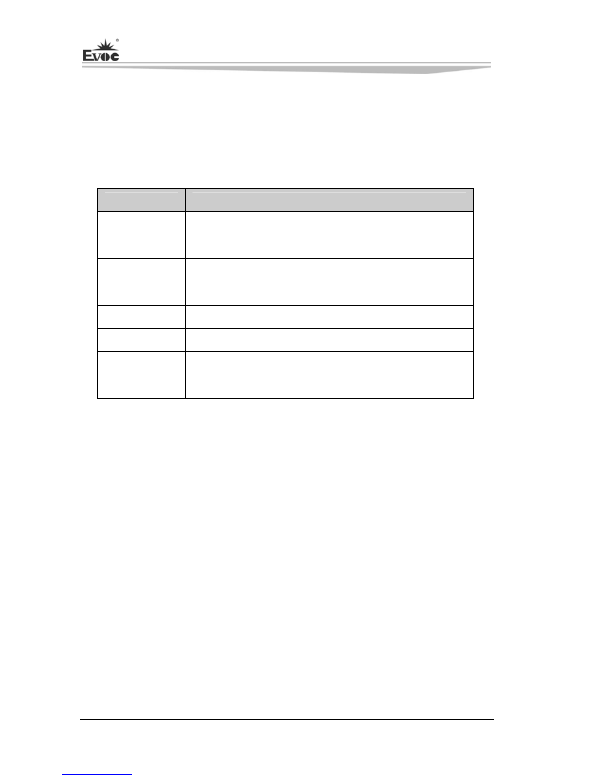
System Resource Managed by BIOS under X86 Platform
We define three kinds of system resources here: I/O port address, IRQ interrupt
number and DMA number.
DMA
Level Function
DMA0
DRAM Refresh
DMA1
Unassigned
DMA2 Floppy Disk
DMA3
Unassigned (sometimes used for hard disk)
DMA4
Used for DMAC Cascade
DMA5
Unassigned
DMA6
Unassigned
DMA7
Unassigned
APIC
Advanced programmable interrupt controller. Most motherboards above P4 level
support APIC and provide more than 16 interrupt sources, like IRQ16 - IRQ23; while
some others can have up to 28 interrupt sources, such as motherboard supporting
PCI-X. However, relevant OS are required to enable that function, and currently, only
the OS above Windows 2000 could support that function.
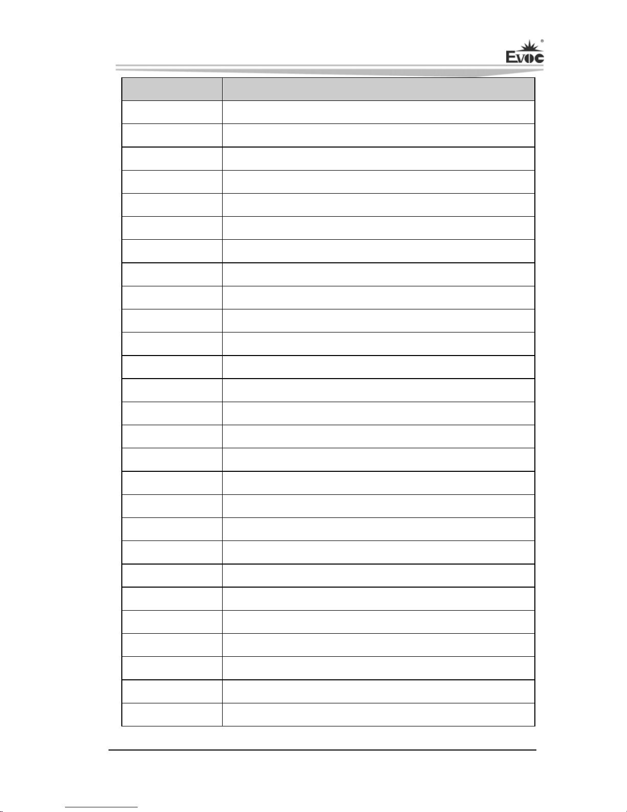
IO Port Address
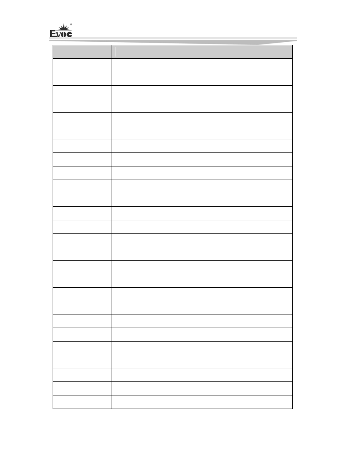
There is 64K for the system I/O address space. Each peripheral will occupy portion of
the space. The table below shows the I/O address assignments for part of the devices
of the CPU card. As the address of PCI device (e.g. PCI network card) is configured
by software, it is not listed in this table.
Page 44
Chapter 3 BIOS Setup
EC0-1814(B) - 39 -
Address Device Description
000h - 00Fh
DMA Controller #1
000h - CF7h
PCI Bus
010h - 01Fh
Carrier Resource
020h - 021h
Programmable Interrupt Controller #1
022h - 03Fh
Carrier Resource
040h - 043h
System Timer
044h - 05Fh
Carrier Resource
060h
Standard 101/102 Key or Microsoft Natural PS/2 Keyboard
061h
System speaker
062h – 063h
Carrier Resource
064h
Standard 101/102 Key or Microsoft Natural PS/2 Keyboard
065h - 06Fh
Carrier Resource
070h - 071h
Real Time Clock, NMI
072h – 07Fh
Carrier Resource
080h
Carrier Resource
081h - 083h
DMA Controller #2
084h - 086h
Carrier Resource
087h
DMA Controller #3
088h
Carrier Resource
089h - 08Bh
DMA Controller #4
08Ch - 08Eh
Carrier Resource
08Fh
DMA Controller #5
090h - 09Fh
Carrier Resource
0A0h - 0A1h Programmable Interrupt Controller #2
0A2h – 0BFh Carrier Resource
0C0h - 0DFh
DMA Controller #6
0E0h - 0EFh
Carrier Resource
Page 45
Chapter 3 BIOS Setup
- 40 - EC0-1814(B)
Address Device Description
0F0h - 0FFh
Numeric data processor
170h - 177h
Slave IDE
1F0h - 1F7h
Master IDE
200h - 207h
COM3
208h – 20Fh
COM4
210h - 217h
COM5
218h – 21Fh
COM6
274h – 277h ISAPNP Read Data Port
279h ISAPNP Read Data Port
2F8h - 2FFh COM2
376h Slave IDE(dual FIFO)
378h - 37Fh LPT1
3B0h – 3BBh Intel(R) G41 Express Chipset Family
3C0h – 3DFh Intel(R) G41 Express Chipset Family
3F0h – 3F5h Standard Floppy Disk Controller
3F6h Master IDE(dual FIFO)
3F7h Standard Floppy Disk Controller
3F8h - 3FFh COM1
400h - 41Fh
Intel(R) N10 ICH7 Family SMBus Controller – 27DA
480h – 4BFh Carrier Resource
4D0h –4D1h Carrier Resource
800h – 87Fh Carrier Resource
A00h – A0Fh Carrier Resource
A10h – A1Fh Carrier Resource
A79h ISAPNP Read Data Port
0D00h-FFFFh PCI bus
Page 46
Chapter 3 BIOS Setup
EC0-1814(B) - 41 -
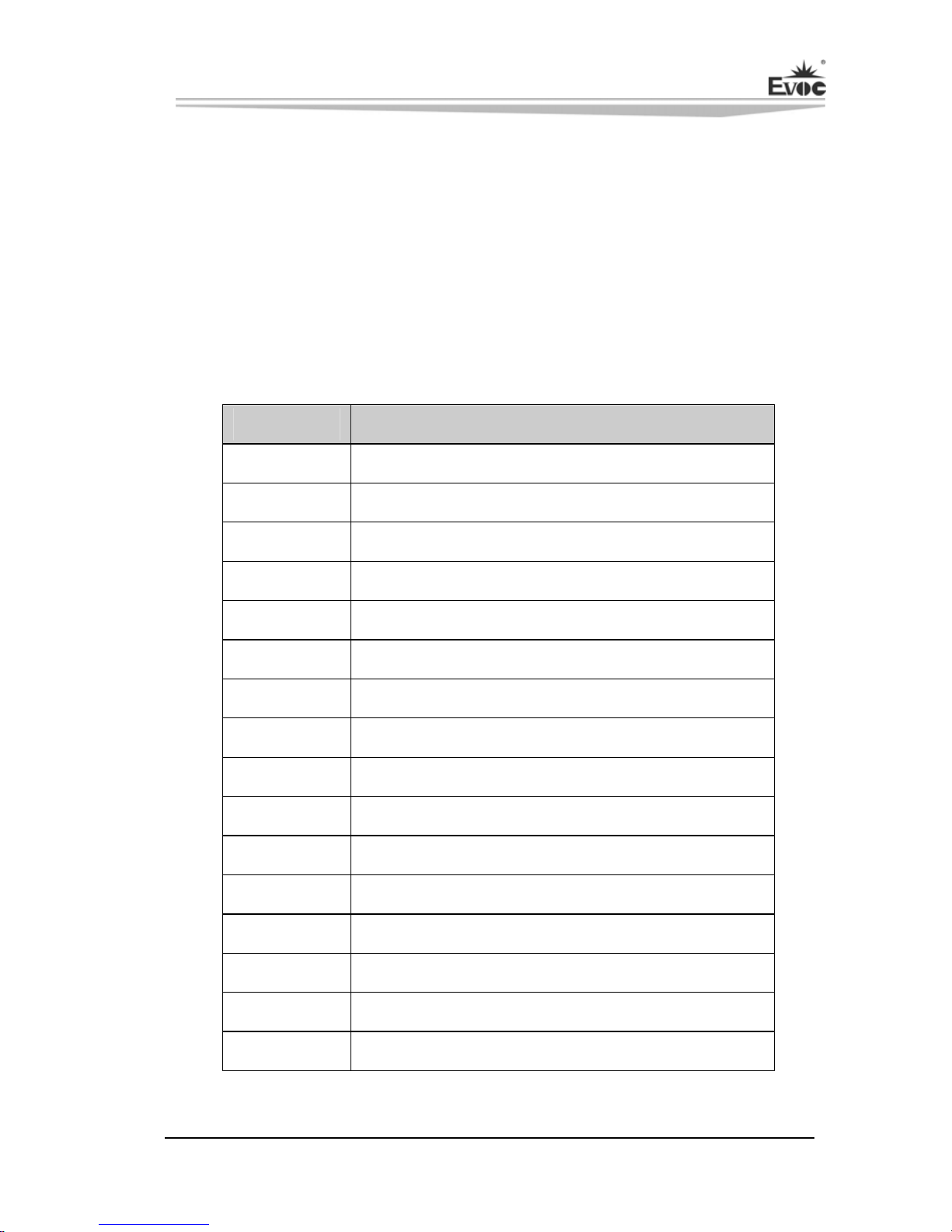
IRQ Assignment Table
There are 15 interrupt sources of the system. Some are occupied by the system
devices. Only the ones that are not occupied can be assigned to other devices. ISA
device requests exclusive use of its interrupt. Only the plug and play ISA devices can
be assigned by the BIOS or the OS. And several PCI devices share one interrupt,
which is assigned by BIOS or OS. Interrupt assignment of some devices of X86
platform is shown in the table below, but it does not show the interrupt source
occupied by the PCI devices.
Level Function
IRQ0 System Timer
IRQ1 Standard 101/102 Key or Microsoft Keyboard
IRQ2 Reserved
IRQ3 COM#2
IRQ4 COM#1
IRQ5 Reserved
IRQ6 Standard Floppy Disk Controller
IRQ7 Parallel Port#1
IRQ8 System CMOS/Real Time Clock
IRQ9 Microsoft ACPI-Compliant System
IRQ10 COM#3 ~ COM#6
IRQ11
Reserved
IRQ12
Reserved
IRQ13 Numeric data processor
IRQ14 Master IDE
IRQ15 Slave IDE
Page 47

Chapter 4 Install the Drivers
- 42 - EC0-1814(B)
Chapter 4 Install the Drivers
Regarding the driver program of this product, please refer to the enclosed CD.
Page 48

Appendix
EC0-1814(B) - 43 -
Appendix
Watchdog Programming Guide
The board provides a programmable watchdog timer (WDT) up to 255 levels and
timed by minute or second. Watchdog timeout event can be programmed to reset
system or generate maskable interrupts.
The available IRQ numbers for this board are: 3, 4, 5, 7, 9, 10 and 11.
Please modify the corresponding IRQ number in PCIPnP of BIOS Setup
interface into “Reserved” before using.
The following describes WDT program in C language. The steps to program WDT are
listed as follows:
Enter WDT programming mode;
Set WDT operating mode/enable WDT/disable WDT.
(1) Enter WDT Programming Mode
/*
Description: the function, PreInitWDT, is used to initialize the registers relevant
to WDT; please invoke the function before configuring and using WDT.
Input: none
Output: none
Note: none
*/
#define INDEX_PORT 0x2E
#define DATA_PORT 0x2F
VOID PreInitWDT()
{
outportb(INDEX_PORT, 0x87);
outportb(INDEX_PORT, 0x87);
outportb(INDEX_PORT, 0x07);
Page 49
Appendix
- 44 - EC0-1814(B)
outportb(DATA_PORT, 0x08);
outportb(INDEX_PORT, 0x30);
outportb(DATA_PORT, 0x01);
}
(2) Configure the WDT operating mode to enable or disable WDT
/*
Description: the function, SetWDT, is used to configure the parameter required
when configuring WDT to enable or disable WDT.
Input: Wmode: 0 - Configure WDT to reset mode
IRQ_NO - Configure WDT to interrupt mode. Please
replace the constant IRQ_NO with the interrupt number
need to be used. The available range of the interrupt number
has been listed in the beginning of this chapter
Wtime: 0 - Configure WDT to time by minute
1 - Configure WDT to time by second
Timeout: 0 - disable WDT
TIME_OUT_VALUE - Enable WDT. Please replace the
constant TIME_OUT_VALUE with the unit number of
timeout value (0x01 ~ 0xFF)
Note:
*/
SetWDT(int Wmode, int Wtime, int Timeout)
{
unsigned char oldval;
outportb(INDEX_PORT,0x2d);
oldval = inportb(DATA_PORT);
If (Wmode == 0)
{
oldval &= 0xfe;
Page 50
Appendix
EC0-1814(B) - 45 -
outportb(DATA_PORT, oldval);
}
else
{
oldval |= 0x01;
outportb(DATA_PORT, oldval);
outportb(INDEX_PORT,0xf7);
outportb(DATA_PORT, Wmode);
}
outportb(INDEX_PORT,0xf5);
If (Wtime == 0)
outportb(DATA_PORT,0x08);
Else
outportb(DATA_PORT,0x00);
outportb(INDEX_PORT,0xf6);
If (Timeout == 0)
outportb(DATA_PORT,0x00);
Else
outportb(DATA_PORT, Timeout);
}
Digital IO Programming Guide
The board provides 8-channel programmable digital IO pins, four for input while the
other four for output. The following provides digital I/O program in C language;
please follow the steps below to implement digital I/O programming:
(The GPIO1 ~ 8 described in the Users’ Manual are corresponding with GPIO30, 31,
34, 35, 36, 37, 20 and 21 of the Super IO; take GPIO1, 2, 3 and 4 setting to input (it is
read-only for input) and GPIO5, 6, 7 and 8 setting to output (it is read and write for
output) as an example).
Initialize digital I/O
Input/output program
(1) Initialize Digital I/O:
#define INDEX_PORT 0x2E
Page 51
Appendix
- 46 - EC0-1814(B)
#define DATA_PORT 0x2F
VOID PreInitGPIO()
{
outportb(INDEX_PORT,0x87);
outportb(INDEX_PORT,0x87);
outportb(INDEX_PORT,0x07);
outportb(DATA_PORT,0x09);
outportb(INDEX_PORT,0x30);
outportb(DATA_PORT,0x03); //Enable GPIO2 and GPIO3 series.
}
outportb(INDEX_PORT,0xF8);
outportb(DATA_PORT,0x0);
outportb(INDEX_PORT,0x29);
Temp_val=(inportb(DATA_PORT)|0x02)&0xfb;
outportb(DATA_PORT, Temp_val); //GP21,GP20 select as gpio
Note: the multifunctional GPIO shall be initialized to GPIO function.
(2) Input/output program:
outportb(INDEX_PORT, 0xE3);
Temp_val=(inportb(DATA_PORT))&0xfc;
outportb (DATA_PORT, Temp_val) ;// GPIO20 and 21, i.e. GPIO7 and 8,
are set to output.
outportb(INDEX_PORT, 0xE4);
Temp_val=(inportb(DATA_PORT))&0xfc;
outportb (DATA_PORT, Temp_val) ;// GPIO7 and 8 are set to low level.
outportb(INDEX_PORT, 0xF0);
Temp_val=(inportb(DATA_PORT)|0x33)&0x3f;
outportb (DATA_PORT, 0x3F);// GPIO30, 31, 34 and 35, i.e. GPIO1, 2,
3 and 4, are set to input; //GPIO36 and 37, i.e. GPIO5 and 6 are set to output.
outportb(INDEX_PORT, 0xF1);
Temp_val=(inportb(DATA_PORT))&0x3f;
outportb (DATA_PORT, Temp_val) ;// GPIO5 and 6 are set to low level.
(3) Disable Programming
outportb(0x2e,0xaa);
Page 52
Appendix
EC0-1814(B) - 47 -
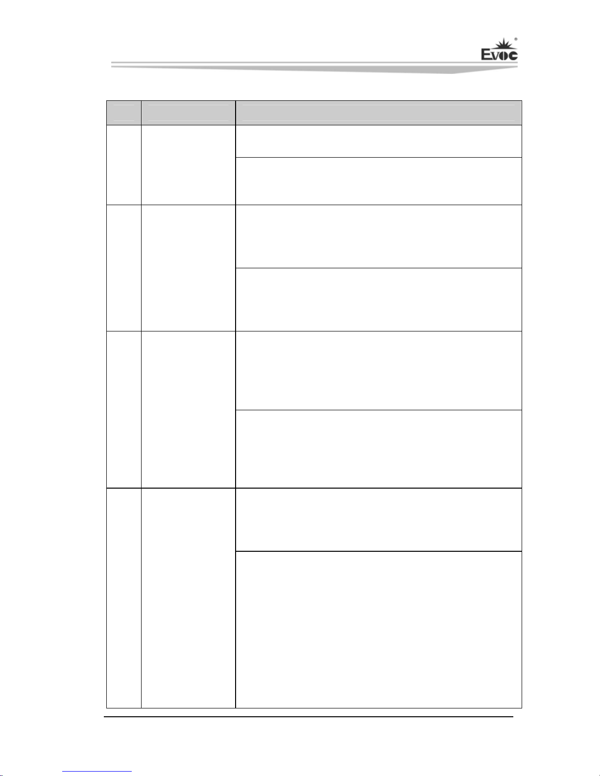
Troubleshooting and Solutions
NO. Phenomenon Troubleshooting and Solution
Analysis: it could be the problem of the CMOS battery.
1
BIOS setting
cannot be saved
Solution: measure the CMOS battery with a multi-meter;
if the voltage is insufficient, replace the battery; re-set the
BIOS and save again.
Analysis: it may be caused by poor connection. Remove
the power plug from power socket on motherboard, you
may find that certain pin of the motherboard power has
been collapsed to one side after some forceful insertion.
2
The computer
can only be
powered-on
occasionally
Solution: power off the computer and remove the power
plug; erect the bended power pin with tweezers and
re-insert in the power socket. Reboot the computer and
test for several times until the problem no longer exits.
Analysis: A USB flash drive is a high-speed USB2.0;
when connecting with the computer, it prompts that a
high-speed device has been connected with a low-speed
connector, which indicates that the connector on
motherboard is regarded as a USB1.1 port.
3
When
connecting with
a USB flash
drive, the system
prompts that a
high-speed
device has been
connected with a
low-speed
connector.
Solution: enable the USB high-speed transmission mode
on the motherboard. Different motherboards may have
different settings. Change the FULLSPEED option to
HISPEED in USB device option.
Analysis: it could result from improper operation when
inserting or removing the memory and cause abnormal
operation of the components on the motherboard. Focus
on the circuit related to the memory on the motherboard.
4
The screen has
no display after
replacing with a
new memory
and cannot enter
system; even
when the former
memory is
re-installed, the
system cannot
be booted as
well.
Solution: check the hardware such as memory, video card
first; if it shows that the hardware are all OK, then check
the circuit around the memory slot on motherboard
carefully; you may find that the two pins connected with
the gold finger in the first memory slot are shorted while
the second memory slot is normal, then you may know
that there is short circuit in the first memory slot. Remove
the two pins to their original location with tweezers
carefully, insert the memory, reboot the system and the
system will be booted smoothly.
Page 53
Appendix
- 48 - EC0-1814(B)
Analysis: the data cable of the hard disk may get knocked
when installing the CD-ROM, which leads to poor
connection of the hard disk data cable, or the master and
slave jumpers on hard disk and CD-ROM are wrongly
set.
5
The system
cannot be
booted after
replacing a
CD-ROM.
Solution: check the data cable of the hard disk and the
IDE connectors on hard disk and motherboard first; if
there are no problems, then check the master and slave
jumper setting. You may find that the hard disk and
CD-ROM are connected with different data cables while
their jumpers are all set to master; thus, the hard disk
cannot be booted. Set the CD-ROM jumper to slave and
then re-install it.
Analysis: make sure the PCI card functions normally;
re-insert the PCI card or insert it into another PCI slot to
see whether it is normal; find out the power type in use
(AT or ATX); find out users’ requirement for the PCI card
voltage.
6
No PCI card can
be detected after
entering the
system.
Solution: if the PCI card functions abnormally, replace it
with a new one; if it functions normally when re-inserted
or inserted in another PCI slot, then there is something
wrong between the PCI card and the slot. If AT power is
adopted and the PCI card requires 3.3V voltage, then the
AT power shall be replaced with ATX power because AT
power cannot provide 3.3V voltage. (Suggestion: when
purchasing power supplies, please check whether the PCI
card in use requires 3.3V voltage or not).
Analysis: devices are not connected; no drivers are
loaded; devices are broken.
7
No peripheral
devices can be
detected.
Solution: check whether the cable between the device and
the motherboard is normal; if it is normal, replace it with
a new cable to make sure the connection is OK. Re-install
the device driver and check whether it can be recognized;
check whether the device is normal; if the device is
normal, then check whether the device is compatible with
the motherboard.
 Loading...