

Page 1

BT-MSOII
Manual
Revision 1.2 – 2016/10/25
CONFIDENTIAL INFORMATION
Everint Co., Ltd..
Page 2

List of Contents
1. General .......................................................................................................... 3
1.1 Overview ................................................................................................................................. 3
1.2 Features ................................................................................................................................... 4
1.3 Application .............................................................................................................................. 4
1.4 Pin Configuration ..................................................................................................................... 5
1.5 Device Terminal Functions ....................................................................................................... 6
1.6 Package Dimensions & Land Pattern ........................................................................................ 7
2. Characteristics ............................................................................................... 9
2.1 Electrical Characteristics .......................................................................................................... 9
2.2 RF Characteristics ................................................................................................................... 10
2.3 Antenna Characteristics ......................................................................................................... 11
3. Terminal Description ................................................................................... 12
3.1 UART Interface ....................................................................................................................... 12
3.2 SPI Interface (Debug only) ...................................................................................................... 12
3.3 I2C Interface .......................................................................................................................... 12
4. Reset, RST# .................................................................................................. 13
2
Page 3
1. General
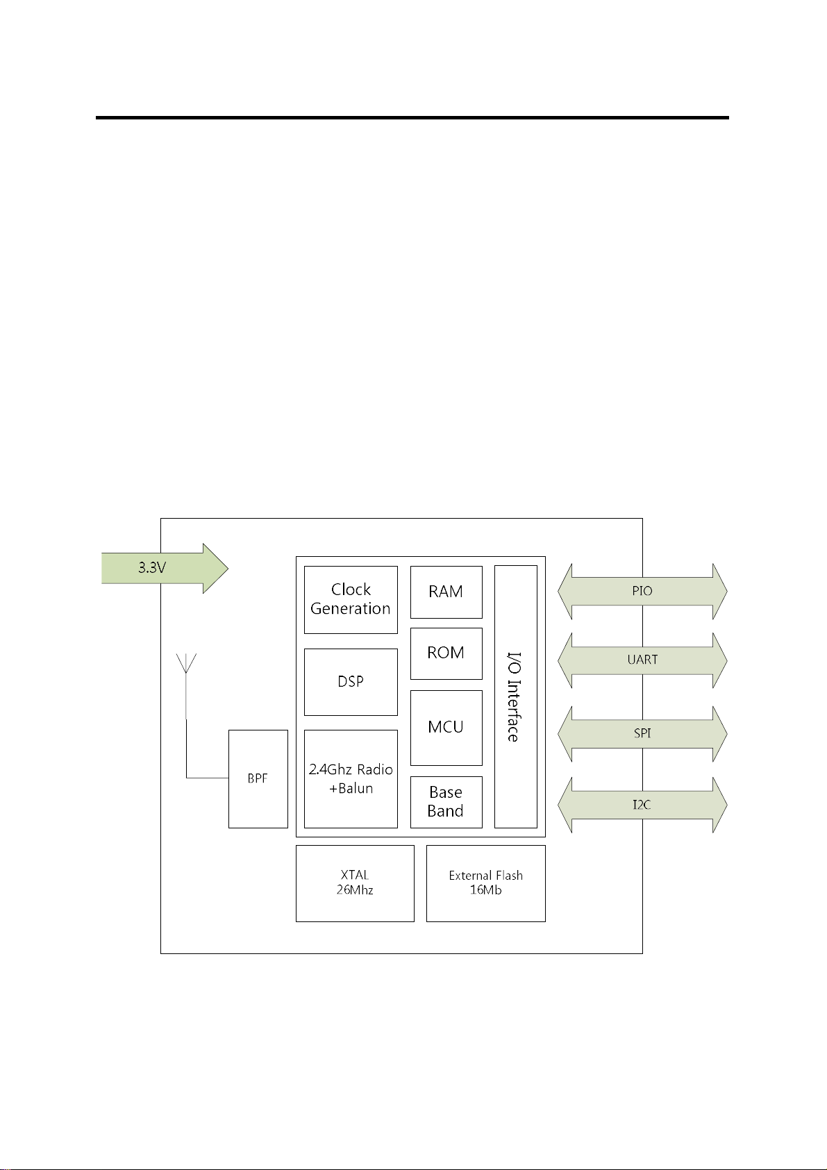
1.1 Overview
This specification covers Bluetooth module which complies with Bluetooth specification
version 4.1 and integrates RF & Baseband controller in small package. This Module has
deployed CSR’s CSRB5341 chipset.
All detailed specification including pin outs and electrical specification may be changed
without notice.
3
Page 4

1.2 Features
■ Bluetooth® v4.1 specification compliant
■ Radio includes integrated balun and typical RF
performance of 6 dBm transmit power and -87 dBm
receive sensitivity
■ 80 MHz RISC MCU
■ Programmable DSP with 4K x 32-bit program
■ Serial interfaces: UART , I²C and SPI (debug only)
■ 4 general purpose PIOs.
■ Integrated to 16Mbit external Flash memory
■ Power‑on‑reset detects low supply voltage
■ Competitive Size
BT-MSOII : 28mm x 18mm x 2.8mm : 44Pin
■ Operating temperature range (MAX -20℃ ~ 70℃)
1.3 Application
■ Mobile Printer
■ POS system
4
Page 5

1.4 Pin Configuration
GND
GND
GND
GND
NC
nRESET
BT_STATUS
NC
NC
44
1
2
3
4
5
6
7
8
9
GND
43
GND
42
NC
41
GND
40
GND
39
NC
38
NC
37
GND
36
DEBUG_SPI_CS#
35
DEBUG_SPI_MISO
34
GND
33
DEBUG_SPI_SEL
NC
3.3V
3.3V
GND
GND
GND
10
11
12
13
14
15
16 17 18 19 20 21 22 23 24
NC
NC
TXD
RXD
nCTS
NC
Pin Configuration (TOP VIEW)
32
DEBUG_SPI_MOSI
31
DEBUG_SPI_CLK
30
NC
29
APPLE_SDA
28
APPLE_SCL
27
GND
25 26
NC
RTS_CTL
AT_CMD
NC
BT_DUT
5
Page 6
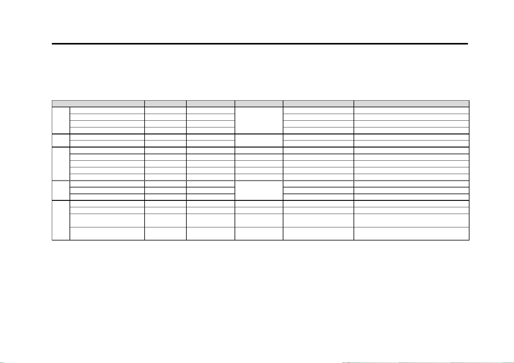
1.5 Device Terminal Functions
PIO
I2C
Interface
SPI
Interface
UART
Interface
Other
Pins
Function
PIO[13]
PIO[14]
PIO[15]
PIO[16]
SDA
SCL
SPI_MISO
SPI_MOSI
SPI_CS#
SPI_CLK
SPI_SEL
UART_RX
UART_TX
UART_CTS
3V3
RESET
GROUND
NC NC
Pin Name Pin No. Pin type Descriptio n Note
BT_DUT 25 BT DUT
BT_STATUS 7 BT_STATUS
AT_CMD 23 AT Command
RTS_CTL 22 RTS Control
APPLE_SDA 29 Apple MFi Chip Inte rface Data
APPLE_SCL 28 Apple MFi Chip Interface Clock
DEBUG_SPI_MISO 35 Output, Weak Pull Down SPI Data Output
DEBUG_SPI_MOSI 32 Input, Weak Pull Down SPI Data Input
DEBUG_SPI_CS# 36 Input, Weak Pull Down Chip Select Active Low
DEBUG_SPI_CLK 31 Input, Weak Pull Down SPI Clock
DEBUG_SPI_SEL 33 Input, Pul l Up SPI Sele ct
RXD 19 UART Data Input
TXD 17 UART Data Output
nCTS 18 UART Clear to Send Active Low
3V3 11,12 Positi ve Powe r Supply
nRESET 6 Input, Stong Pull Up Reset
1,2,3,4,13,14,15,27,34,37
40,41,43,44
5,8,9,10,16,20,21,24,26,30
38,39,42
Bideirection,
Weak Pull Down
Bideirection,
Weak Pull Up
Bidirection
Weak Pull Down
GroundGND
Not Connect
6
Page 7
0.15
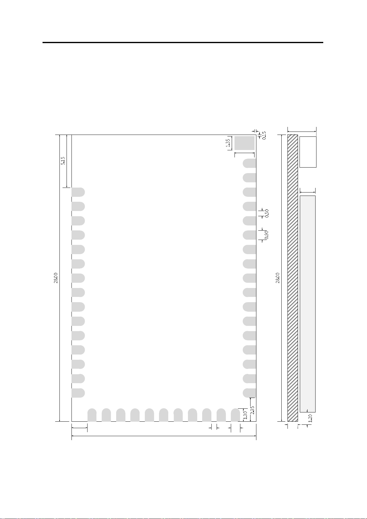
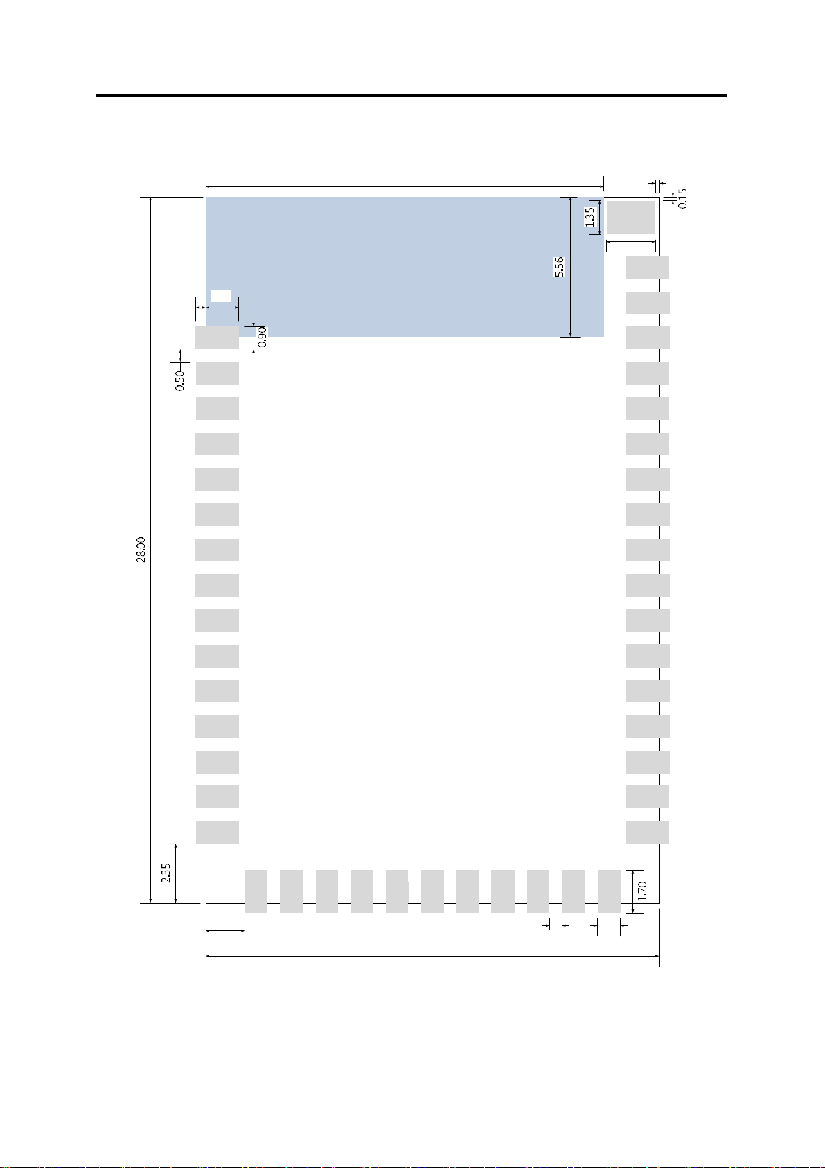
1.6 Package Dimensions & Land Pattern
● unit = mm
● General Tolerances = ±0.2mm
2.80
1.95
1.50
1.55
18.00
0.900.50
1.00
BT-MSOII Dimensions
7
Page 8
0.15
15.80
1.95
ANTENNA AREA
1.30
0.40
1.55
18.00
0.50
0.90
Land Pattern
8
Page 9
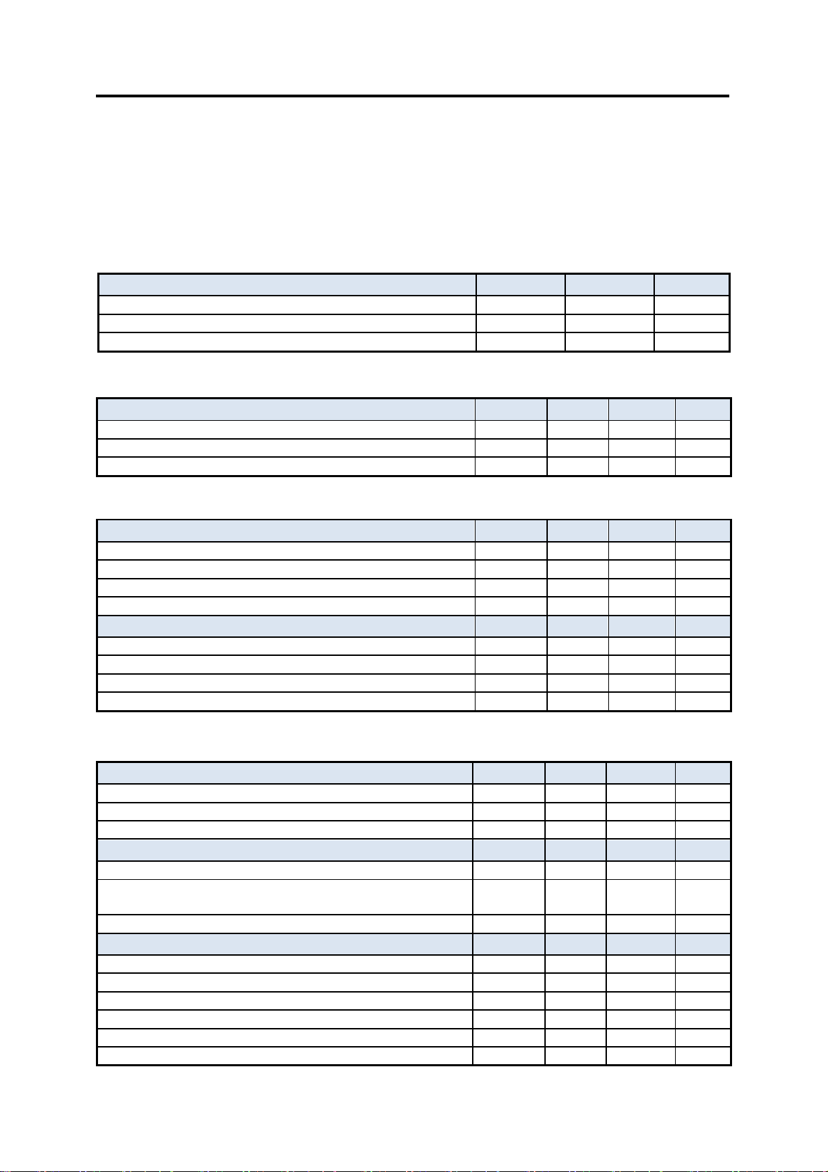
Storage Temperature range
-40 85 °C VDD -
0.4
3.6 V
Other terminal voltages
VSS-0.4 VDD+0.4
V
Operating Temperature range
-20 20 70 °C VDD 2.5 3.3 3.6 V Other terminal voltage
2.5 3.3 3.6 V
Standby current
- 5 - mA Connected current
- 4 - mA
TX current with UART
- 9 23 mA RX
current with UART
- 9 19 mA
Standby current
- 6 - mA Connected current
- 4 - mA
TX current with UART
- 7 27 mA RX
current with UART
- 4 20 mA
VIL
input logic level low
-0.4 - 0.25xVDD
V
VIH
input logic level high
0.7 x
VDD - VDD+0.4
V
Tr/Tf - - 25 ns
VOL
output logic level low, l
OL
= 4.0mA
- -
0.4 V
0.75 x
Tr/Tf - - 5 ns
Strong pull
-up -150 -40 -10 μA Strong pull
-
down
10 40
150 μA Weak pull
-up -5 -1.0 -
0.33 μA Weak pull
-
down
0.33 1 5 μA CI
Input Capacitance
1 - 5 pF
High impedance state (no pulls)
-0.1 0 0.1 μA
2. Characteristics
2.1 Electrical Characteristics
■ Absolute Maximum Ratings
Rating Min Max Unit
■ Recommended Operating Conditions
Operating Condition Min Typ Max Unit
■ Current consumption
Classic (Test Condition : VDD =3.3V, Temp = 25°C, Sniff = 40ms)
BLE (Test Condition : VDD =3.3V, Temp = 25°C, Sniff = 16.25ms)
UART baud rate = 230,400bps
Typ Peak Unit
Typ Peak Unit
■ Digital Terminals
Input Voltage Levels Min Typ Max Unit
Output Voltage Levels Min Typ Max Unit
VOH output logic level high, lOH = -4.0mA
Input and Tristate Currents Min Typ Max Unit
VDD
- - V
9
Page 10
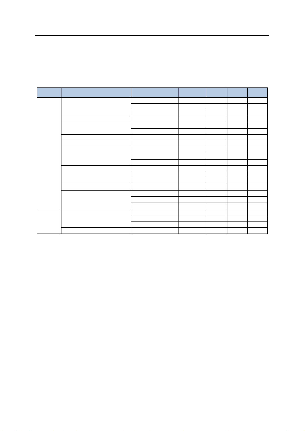
2.2 RF Characteristics
RF Specification Condition Min Typ Max Unit
2.402 - 4.69 - dB
Transmitter
Receiver
Output transmit power
Transmit power density - -6.29 - dBm
Transmit power control
Frequency Range 2401.515 - 2480.485 Mhz
20dB bandwidth for modulation - 925 - Khz
Adjacent channel transmit power
Modulation characteristics
Intial carrier frequency tolerance df0_avg - -13.7 - Khz
One slot packet(DH1) - -4.7 - KHz
Carrier frequency drift
Sensitivity at 0.1% BER for all
basic rate packet types
Maximum input level -20 -5 - dBm
Three slot packet(DH3) - -6.4 - KHz
2.441 - 4.96 - dB
2.480 - 5.15 - dB
Pmin -25.79 - - dBm
Pst 3.88 4.81 - dB
±2MHz - -22.4 - dBm
±3MHz - -48.09 - dBm
±4Mhz - -48.79 - dBm
Δf1avg - 165 - Khz
Δf2_pass_rate - 100 - %
Δf2avg/Δf1avg - 0.93 -
Five slot packet(DH5) - -6.4 - KHz
2.402 -84.6 - dBm
2.441 - -86.9 - dBm
2.480 -86.9 - dBm
10
Page 11
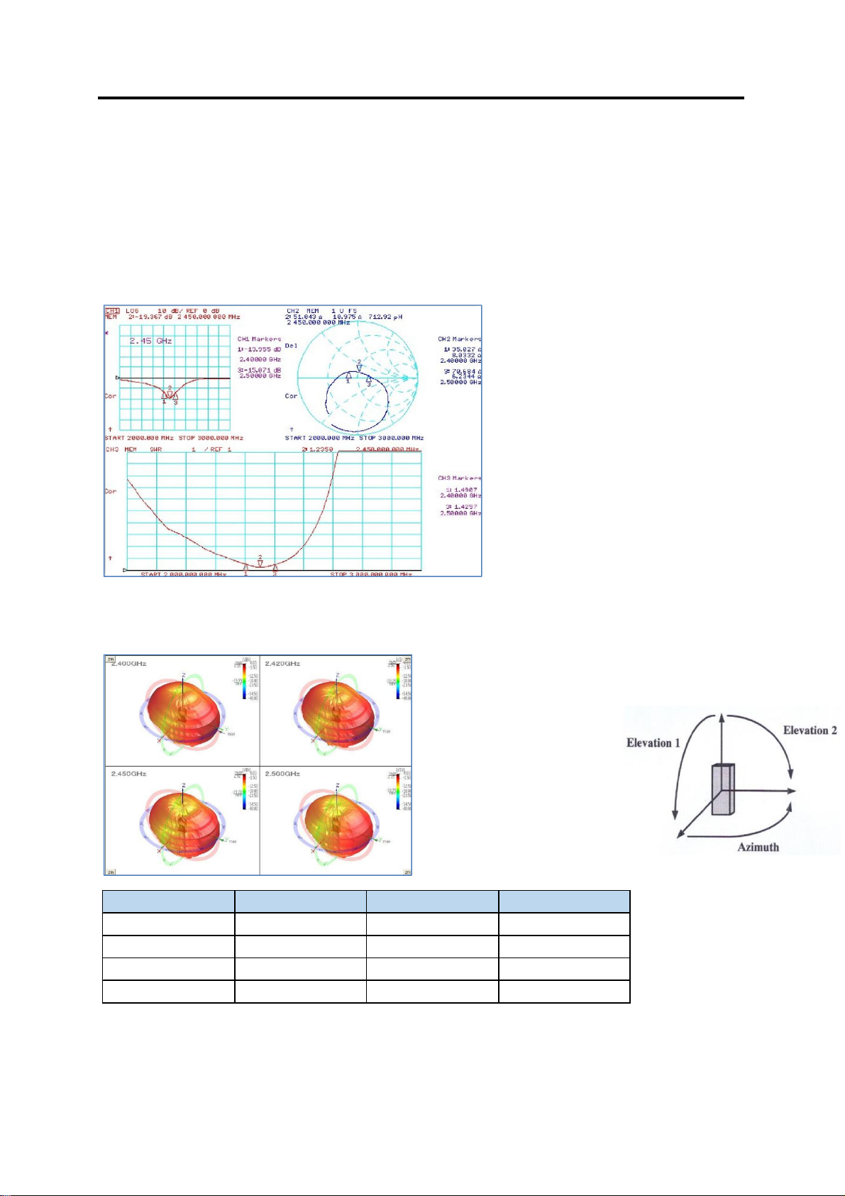
2.3 Antenna Characteristics
The antenna is monopole type of chip antenna. The antenna impedance matching is optimized
for 1 mm ~ 2 mm mother board PCB thickness. The radiation pattern is impacted by the layout of
the mother board. Typically the highest gain is towards GND plane and weakest gain away from the
GND plane.
■ LOG, Smith Chart & VSWR
■ Radiation Gain
Freq(Mhz) Efficiency(%) Avg. Gain(dBi) Peak Gain(dBi)
2400 55.26 -2.58 3.16
2420 56.16 -2.51 3.56
2450 45.52 -3.42 2.92
2500 37.27 -4.29 2.15
11
Page 12

3. Terminal Description
3.1 UART Interface
This is a standard UART interface for communicating with other serial devices.
BT-MSOII UART interface provides a simple mechanism for communicating with other serial devices
using the RS-232 protocol.
When BT-MSOII is connected to another digital device, UART_RX and UART_TX transfer data
between the 2 devices. The remaining a signal, UART_CTS implement optional RS232 hardware flow
control
3.2 SPI Interface (Debug only)
BT-MSOII provides a debug SPI interface for programming, configuring and debugging the BT-MSOII.
Access to this interface is required in production. Ensure the 4 SPI signals externally.
3.3 I2C Interface
BT-MSOII supports a firmware controlled I²C interface to communicate with external Device.
The I²C timing is compliant with the Philips I²C Specification (100 kHz and 400 kHz).
12
Page 13

4. Reset, RST#
BT-MSOII is reset from several sources:
▪ RST# pin
▪ Power-on reset
▪ UART break character
The RST# pin is an active low reset and is internally filtered using the internal low
frequency clock oscillator. CSR recommends applying RST# for a period >5ms.
13
Page 14

■ Notice
This device complies with Part 15 of the FCC Rules. Operation is subject to the
following two conditions:
(1) This device may not cause harmful interference, and
(2) This device must accept any interference received, including interference
that may cause undesired operation.
This device complies with Industry Canada’s licence-exempt RSSs. Operation is
subject to the following two conditions:
(1) This device may not cause interference; and
(2) This device must accept any interference, including interference that may
cause undesired operation of the device
Le présent appareil est conforme aux CNR d'Industrie Canada applicables aux
appareils radio exempts de licence. L'exploitation est autorisée aux deux
conditions suivantes :
(1) l'appareil ne doit pas produire de brouillage, et
(2) l'utilisateur de l'appareil doit accepter tout brouillage radioélectrique subi,
même si le brouillage est susceptible d'en compromettre le fonctionnement.
The module is limited to OEM installation ONLY.
OEM integrators are responsible for ensuring that the end-user has no manual
instructions to remove or install module.
The module is limited to installation in mobile or fixed applications, according to
Part 2.1091(b).
Separate approval is required for all other operating configurations, including
portable configurations with respect to Part 2.1093 and different antenna
configurations.
For a host manufacture’s using a certified modular, if (1) the module’s FCC ID is
not visible when installed in the host, or (2) if the host is marketed so that end
users do not have straightforward commonly used methods for access to remove
the module so that the FCC ID of the module is visible; then an additional
permanent label referring to the enclosed module: “Contains Transmitter
Module FCC ID: 2AKMF-BT-MSOII” or “Contains FCC ID: 2AKMF-BT-MSOII”
must be used. The host OEM user manual must also contain clear instructions on
how end users can find and/or access the module and the FCC ID.
Canada certification label of a module shall be clearly visible at all times when
installed in the host product; otherwise, the host product must be labelled to
display the Canada certification number for the module, preceded by the word
“Contains” or similar wording expressing the same meaning, as follows:
Contains IC : 22266-BTMSOII
14
Page 15
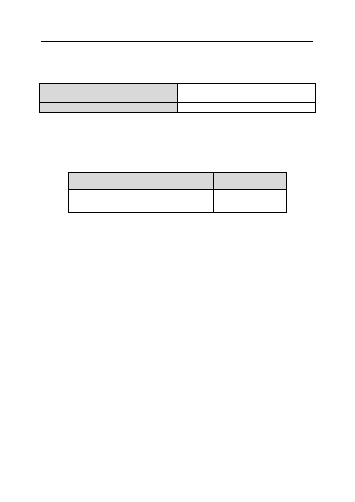
■ Product Information
Model Number BT-MSOII
Product Name Bluetooth Module
Firmware Version 2.0.0
■ Antenna
The MT-MSOII Module has been designed to operate with the following antenna and gains. Use
with other antenna types or with these antenna types at higher gains is strictly prohibited.
Type of Antenna Gain (dBi) Type of Connector
Chip Antenna 3.56
Permanent
integral
■ Warning - U.S.A
i) Changes or modifications not expressly approved by the manufacturer could
void the user's authority to operate the equipment.
ii) Caution: Exposure to Radio Frequency Radiation.
To comply with FCC RF exposure compliance requirements, a separation distance
of at least 20 cm must be maintained between the antenna of this device and all
persons.
Afin de se conformer aux exigences en matière d'exposition aux
rayonnements radioélectriques, une distance de séparation d'au moins 20 cm
doit être maintenue entre l'antenne de cet appareil et toutes les personnes.
15
 Loading...