

Page 1

User’s Manual
ECM-3610/3610L
All-in-One VIA Eden ESP6000 Single Board with LCD, LVDS,
AC97 Audio, & Dual 10/100Base-Tx Ethernet
6th Ed. – 15 November 2004
Part No. 2047361000
Page 2

ECM-3610/3610L
FCC STATEMENT
THIS DEVICE COMPLIES WITH PART 15 FCC RULES. OPERATION IS SUBJECT TO
THE FOLLOWING TWO CONDITIONS:
(1) THIS DEVICE MAY NOT CAUSE HARMFUL INTERFERENCE.
(2) THIS DEVICE MUST ACCEPT ANY INTERFERENCE
RECEIVED INCLUDING INTERFERENCE THAT MAY CAUSE UNDESIRED
OPERATION.
THIS EQUIPMENT HAS BEEN TESTED AND FOUND TO COMPLY WITH THE LIMITS
FOR A CLASS "A" DIGITAL DEVICE, PURSUANT TO PART 15 OF THE FCC RULES.
THESE LIMITS ARE DESIGNED TO PROVIDE REASONABLE PROTECTION
AGAINTST HARMFUL INTERFERENCE WHEN THE EQUIPMENT IS OPERATED IN A
COMMERCIAL ENVIRONMENT. THIS EQUIPMENT GENERATES, USES, AND CAN
RADIATE RADIO FREQUENCY ENERGY AND, IF NOT INSTATLLED AND USED IN
ACCORDANCE WITH THE INSTRUCTION MANUAL, MAY CAUSE HARMFUL
INTERFERENCE TO RADIO COMMUNICATIONS.
OPERATION OF THIS EQUIPMENT IN A RESIDENTIAL AREA IS LIKELY TO CAUSE
HARMFUL INTERFERENCE IN WHICH CASE THE USER WILL BE REQUIRED TO
CORRECT THE INTERFERENCE AT HIS OWN EXPENSE.
Evalue Technology Inc.
Page 3

User’s Manual
Copyright Notice
Copyright 2002, 2003, Evalue Technology Inc., ALL RIGHTS RESERVED.
No part of this document may be reproduced, copied, translated, or transmitted in any
form or by any means, electronic or mechanical, for any purpose, without the prior written
permission of the original manufacturer.
Trademark Acknowledgement
Brand and product names are trademarks or registered trademarks of their respective
owners.
Disclaimer
Evalue Technology Inc. reserves the right to make changes, without notice, to any product,
including circuits and/or software described or contained in this manual in order to
improve design and/or performance. Evalue Technology assumes no responsibility or
liability for the use of the described product(s), conveys no license or title under any
patent, copyright, or mask work rights to these products, and makes no representations or
warranties that these products are free from patent, copyright, or mask work right
infringement, unless otherwise specified. Applications that are described in this manual
are for illustration purposes only. Evalue Technology Inc. makes no representation or
warranty that such application will be suitable for the specified use without further testing
or modification.
Life Support Policy
Evalue Technology’s PRODUCTS ARE NOT FOR USE AS CRITICAL COMPONENTS IN
LIFE SUPPORT DEVICES OR SYSTEMS WITHOUT THE PRIOR WRITTEN APPROVAL
OF Evalue Technology Inc.
As used herein:
1. Life support devices or systems are devices or systems which, (a) are intended for
surgical implant into body, or (b) support or sustain life and whose failure to perform,
when properly used in accordance with instructions for use provided in the labelling,
can be reasonably expected to result in significant injury to the user.
2. A critical component is any component of a life support device or system whose failure
to perform can be reasonably expected to cause the failure of the life support device or
system, or to affect its safety or effectiveness.
Evalue Technology Inc.
Page 4

ECM-3610/3610L
A Message to the Customer
Evalue Customer Services
Each and every Evalue’s product is built to the most exacting specifications to ensure
reliable performance in the harsh and demanding conditions typical of industrial
environments. Whether your new Evalue device is destined for the laboratory or the
factory floor, you can be assured that your product will provide the reliability and ease of
operation for which the name Evalue has come to be known.
Your satisfaction is our primary concern. Here is a guide to Evalue’s customer services.
To ensure you get the full benefit of our services, please follow the instructions below
carefully.
Evalue Technology Inc.
Page 5

User’s Manual
Technical Support
We want you to get the maximum performance from your products. So if you run into
technical difficulties, we are here to help. For the most frequently asked questions, you
can easily find answers in your product documentation. These answers are normally a lot
more detailed than the ones we can give over the phone. So please consult this manual
first.
To receive the latest version of the user manual, please visit our Web site at:
http://www.evalue-tech.com/
If you still cannot find the answer, gather all the information or questions that apply to your
problem, and with the product close at hand, call your dealer. Our dealers are well trained
and ready to give you the support you need to get the most from your Evalue’s products.
In fact, most problems reported are minor and are able to be easily solved over the phone.
In addition, free technical support is available from Evalue’s engineers every business
day. We are always ready to give advice on application requirements or specific
information on the installation and operation of any of our products. Please do not
hesitate to call or e-mail us.
Headquarters
Evalue Technology Inc.
7F, 228, Lian-Cheng Road,
Chung-ho City, Taipei,
Taiwan
Tel: +886-2-82262345
Fax: +886-2-82262777
http://www.evalue-tech.com
E-mail: [email protected]
China Branch Office
Evalue Technology Shanghai Inc.
Room 909, 9F, Section B, No.900,
Yisan Road, Caohejing Hi-tech Park,
Shanghai 200233, China
Tel : +86-21-6470-3454
Fax : +86-21-6470-3454
http://www.evalue-tech.com
E-mail: [email protected]
Europe Branch Office
Evalue Europe A/S
Nordre Strandvej 119C,
3150 Hellebaek,
Denmark
Tel : +45-7025-0310
Fax : +45-4975-5026
http://www.evalue-tech.com
E-mail: [email protected]
US Branch Office
Evalue Technology Inc.
Suite 210, 200 Tornillo Way,
Tinton Falls, NJ 07712
USA
Tel: +732-578-0200
Fax: +732-578-0250
http://www.evalue-tech.com
E-mail: [email protected]
Evalue Technology Inc.
Page 6

ECM-3610/3610L
Product Warranty
Evalue warrants to you, the original purchaser, that each of its products will be free from
defects in materials and workmanship for two years from the date of purchase.
This warranty does not apply to any products which have been repaired or altered by
persons other than repair personnel authorized by Evalue, or which have been subject to
misuse, abuse, accident or improper installation. Evalue assumes no liability under the
terms of this warranty as a consequence of such events. Because of Evalue’s high
quality-control standards and rigorous testing, most of our customers never need to use
our repair service. If an Evalue’s product is defective, it will be repaired or replaced at no
charge during the warranty period. For out-of-warranty repairs, you will be billed
according to the cost of replacement materials, service time, and freight. Please consult
your dealer for more details. If you think you have a defective product, follow these steps:
1. Collect all the information about the problem encountered. (For example, CPU type
and speed, Evalue’s products model name, hardware & BIOS revision number, other
hardware and software used, etc.) Note anything abnormal and list any on-screen
messages you get when the problem occurs.
2. Call your dealer and describe the problem. Please have your manual, product, and
any helpful information readily available.
3. If your product is diagnosed as defective, obtain an RMA (return material authorization)
number from your dealer. This allows us to process your good return more quickly.
4. Carefully pack the defective product, a complete Repair and Replacement Order Card
and a photocopy proof of purchase date (such as your sales receipt) in a shippable
container. A product returned without proof of the purchase date is not eligible for
warranty service.
5. Write the RMA number visibly on the outside of the package and ship it prepaid to
your dealer.
Evalue Technology Inc.
Page 7

User’s Manual
Packing List
Before you begin installing your single board, please make sure that the following
materials have been shipped:
n 1 ECM-3610/3610L All-in-One VIA Eden ESP6000 Computing Module
n 1 Quick Installation Guide
n 1 Audio jacks and USB connector daughter board
n 1 CD-ROM contains the followings:
— User’s Manual (this manual in PDF file)
— Ethernet driver and utilities
— VGA drivers and utilities
— Audio drivers and utilities
n Cable set includes the followings:
— 1 PS/2 keyboard and mouse Y cable (6-pin, Mini-DIN)
— 1 IDE HDD cable (40-pin, pitch 2.54mm)
— 1 FDD cable (34-pin, pitch 2.0mm)
— 1 bracket with one printer port cable (26-pin, pitch 2.0mm) and one serial port
cable (10-pin, pitch 2.0mm)
— 2 flat cables (10-pin, pitch 2.0mm) for connecting the Audio/USB daughter board
to the ECM-3610
If any of these items are missing or damaged, please contact your distributor or sales
representative immediately.
Evalue Technology Inc.
Page 8

ECM-3610/3610L
1. MANUAL OBJECTIVES ............................................................................................ 1
2. INTRODUCTION........................................................................................................ 1
2.1 System Overview................................................................................................... 1
2.2 System Specifications .......................................................................................... 2
2.3 Architecture Overview .......................................................................................... 5
2.3.1 VIA Eden™ Processor................................................................................................ 6
2.3.2 VIA VT8606 North Bridge............................................................................................ 6
2.3.3 VIA VT82C686B South Bridge.................................................................................. 11
2.3.4 Realtek RTL8139C Ethernet Controller..................................................................... 13
2.3.5 Intel 82559ER Ethernet Controller (Optional)............................................................ 13
2.3.6 Compact Flash Interface........................................................................................... 14
3. HARDWARE CONFIGURATION............................................................................. 15
3.1 Installation Procedure......................................................................................... 15
3.2 Safety Precautions.............................................................................................. 15
3.2.1 Warning! ................................................................................................................... 15
3.2.2 Caution!..................................................................................................................... 15
3.3 Installing DRAM (SODIMMs)............................................................................... 16
3.3.1 System Memory ........................................................................................................ 16
3.3.2 Memory Installation Procedures................................................................................16
3.4 Jumper & Connector........................................................................................... 17
3.4.1 Jumper & Connector Layout ..................................................................................... 17
3.5 Jumper and Connector List................................................................................ 18
3.6 Setting Jumpers .................................................................................................. 20
3.6.1 Clear CMOS (J4)....................................................................................................... 20
3.6.2 COM2 RS-232/422/485 Select (J5, J6)..................................................................... 21
3.6.3 AT/ATX Power Select (ATATX1)............................................................................... 21
3.7 Connector Definitions......................................................................................... 22
3.7.1 Pin Header Serial Port 2 Connector in RS-232 Mode (CM1)..................................... 22
3.7.2 Serial Port 2 with External DB9 Connector (CM1)..................................................... 22
3.7.3 Signal Description – Serial Port 2 – COM2 in RS-232 Mode (CM1)......................... 22
3.7.4 Pin Header Serial Port 2 Connector in RS-422 Mode (CM1)..................................... 23
3.7.5 Signal Description – Serial Port 2 – COM2 in RS-422 Mode (CM1)......................... 23
3.7.6 Pin Header Serial Port 2 Connector in RS-485 Mode (CM1)..................................... 23
3.7.7 Signal Description – Serial Port 2 – COM2 in RS-485 Mode (CM1).......................... 24
3.7.8 Serial Port 1 with External DB9 Connector (CM2)..................................................... 24
3.7.9 Signal Description – Serial Port 1 – COM1 in RS-232 Mode (CM2).......................... 25
3.7.10 Secondary LCD Panel Connector (CN1)................................................................... 25
3.7.11 Primary LCD Panel Connector (CN2)........................................................................ 26
3.7.12 Signal Description – Primary & Secondary LCD Panel Connector (CN2, CN1) ........ 26
Evalue Technology Inc.
Page 9

User’s Manual
3.7.13 Signal Configuration – DSTN Displays...................................................................... 27
3.7.14 Signal Configuration – TFT Displays......................................................................... 28
3.7.15 PC/104 Connector (CN3, CN4).................................................................................29
3.7.16 Signal Description – PC/104 Connector (CN3, CN4) ................................................ 30
3.7.17 IDE Connector (CN5)................................................................................................ 34
3.7.18 Signal Description – IDE Connector (CN5)................................................................ 35
3.7.19 System Fan Connector (CN6)...................................................................................35
3.7.20 Audio Connector (CN7)............................................................................................. 35
3.7.21 Signal Description – Audio Connector (CN7)............................................................ 36
3.7.22 CD-ROM Audio Input Connector (CN8)..................................................................... 36
3.7.23 Signal Description – CD-ROM Audio Input Connector (CN8).................................... 36
3.7.24 IrDA Connector (CN9)...............................................................................................36
3.7.25 Signal Description – IrDA Connector (CN9) .............................................................. 36
3.7.26 10/100BASE-Tx Ethernet Connector (CN10, CN11).................................................37
3.7.27 Signal Description – 10/100Base-Tx Ethernet Connector (CN10, CN11).................. 37
3.7.28 Floppy Connector (FLP1).......................................................................................... 37
3.7.29 Signal Description – Floppy Connector (FLP1)......................................................... 38
3.7.30 ATX Power Connector (J1) ....................................................................................... 39
3.7.31 ATX Soft-power Bottom (J2)..................................................................................... 39
3.7.32 Signal Description – ATX Soft-power Bottom (J2)..................................................... 39
3.7.33 LCD Inverter Connector (J3)..................................................................................... 39
3.7.34 Signal Description – LCD Inverter Connector (J3)..................................................... 39
3.7.35 Keyboard and PS/2 Mouse Connector (KB1)............................................................ 40
3.7.36 Signal Description – Keyboard & PS/2 Mouse Connectors (KB1)............................. 40
3.7.37 Parallel Port Connector (PNT1)................................................................................. 40
3.7.38 DB25 Parallel Port Connector (PNT1)....................................................................... 41
3.7.39 Signal Description – Parallel Port Connector (PNT1)................................................42
3.7.40 Auxiliary Power Connector (PWR1).......................................................................... 42
3.7.41 Power Connector (PWR2)......................................................................................... 42
3.7.42 USB Connector (USB1)............................................................................................. 43
3.7.43 Signal Description – USB Connector (USB1)............................................................ 43
3.7.44 CRT Connector (VGA1) ............................................................................................ 44
3.7.45 Signal Description – CRT Connector (VGA1)............................................................ 44
3.7.46 LCD Backlight Brightness Adjustment Connector (VR1)........................................... 45
3.7.47 STN LCD Contrast Adjustment Connector (VR2)...................................................... 45
4. AWARD BIOS SETUP............................................................................................. 46
4.1 Starting Setup...................................................................................................... 46
4.2 Using Setup ......................................................................................................... 47
4.2.1 Navigating Through The Menu Bar........................................................................... 47
4.2.2 To Display a Sub Menu............................................................................................. 47
4.3 Getting Help......................................................................................................... 48
4.4 In Case of Problems............................................................................................ 48
4.5 Main Menu............................................................................................................ 48
4.5.1 Setup Items............................................................................................................... 49
4.5.2 Standard CMOS Setup ............................................................................................. 51
4.5.3 Advanced BIOS Features ......................................................................................... 54
4.5.4 Advanced Chipset Features...................................................................................... 58
4.5.5 Integrated Peripherals............................................................................................... 62
Evalue Technology Inc.
Page 10

ECM-3610/3610L
4.5.6 Power Management Setup........................................................................................ 66
4.5.7 PnP/PCI Configuration Setup.................................................................................... 69
4.5.8 Frequency / Voltage Control ..................................................................................... 71
4.5.9 Load Fail-Safe Defaults ............................................................................................ 72
4.5.10 Load Optimized Defaults........................................................................................... 72
4.5.11 Supervisor / User Password Setting.......................................................................... 73
4.5.12 Exit Selecting ............................................................................................................ 74
5. DRIVER INSTALLATION......................................................................................... 76
5.1 Driver Installation for Ethernet Adapter ............................................................ 76
5.1.1 Windows 9x Ethernet Installation..............................................................................76
5.1.2 Windows NT 4.0 Ethernet Installation....................................................................... 83
5.1.3 Windows 2000 Ethernet Installation.......................................................................... 93
5.2 Driver Installation for Display Adapter............................................................ 102
5.2.1 Windows 9x............................................................................................................. 102
5.2.2 Windows NT 4.0 Display Installation.......................................................................107
5.2.3 Windows 2000 Display Installation.......................................................................... 111
5.3 Driver Installation for Audio Adapter............................................................... 118
5.3.1 Windows 9x............................................................................................................. 118
5.3.2 Windows NT 4.0 Audio Installation ......................................................................... 123
5.3.3 Windows 2000 Audio Installation............................................................................ 129
6. MEASUREMENT DRAWING................................................................................. 132
APPENDIX A: BIOS REVISIONS ................................................................................... 133
APPENDIX B: SYSTEM RESOURCES.......................................................................... 134
Memory Map........................................................................................................................ 134
I/O – Map............................................................................................................................. 135
Interrupt Usage.................................................................................................................... 136
DMA-channel Usage............................................................................................................ 137
APPENDIX C: PROGRAMMING THE WATCHDOG TIMER.......................................... 138
Introduction.......................................................................................................................... 138
Programming Watchdog Timer............................................................................................ 138
Demo Program 1 (Micro-Assembly Language) .................................................................... 139
Demo Program 2 (C Language) ........................................................................................... 141
APPENDIX D: AWARD BIOS POST MESSAGES ......................................................... 143
POST Beep ................................................................................................................. 143
Error Messages .......................................................................................................... 143
CMOS BATTERY HAS FAILED........................................................................................... 143
CMOS CHECKSUM ERROR ............................................................................................... 143
DISK BOOT FAILURE, INSERT SYSTEM DISK AND PRESS ENTER ............................... 143
DISKETTE DRIVES OR TYPES MISMATCH ERROR - RUN SETUP ................................. 143
DISPLAY SWITCH IS SET INCORRECTLY........................................................................ 144
DISPLAY TYPE HAS CHANGED SINCE LAST BOOT........................................................ 144
Evalue Technology Inc.
Page 11

User’s Manual
EISA Configuration Checksum Error PLEASE RUN EISA CONFIGURATION UTILITY....... 144
EISA Configuration Is Not Complete PLEASE RUN EISA CONFIGURATION UTILITY....... 144
ERROR ENCOUNTERED INITIALIZING HARD DRIVE....................................................... 144
ERROR INITIALIZING HARD DISK CONTROLLER ............................................................ 144
FLOPPY DISK CNTRLR ERROR OR NO CNTRLR PRESENT........................................... 144
Invalid EISA Configuration PLEASE RUN EISA CONFIGURATION UTILITY...................... 145
KEYBOARD ERROR OR NO KEYBOARD PRESENT........................................................ 145
Memory Address Error at .................................................................................................... 145
Memory parity Error at ......................................................................................................... 145
MEMORY SIZE HAS CHANGED SINCE LAST BOOT ........................................................ 145
Memory Verify Error at ........................................................................................................ 145
OFFENDING ADDRESS NOT FOUND................................................................................ 145
OFFENDING SEGMENT:..................................................................................................... 145
PRESS A KEY TO REBOOT ............................................................................................... 146
PRESS F1 TO DISABLE NMI, F2 TO REBOOT.................................................................. 146
RAM PARITY ERROR - CHECKING FOR SEGMENT ........................................................ 146
Should Be Empty But EISA Board Found PLEASE RUN EISA CONFIGURATION UTILITY146
Should Have EISA Board But Not Found PLEASE RUN EISA CONFIGURATION UTILITY146
Slot Not Empty.....................................................................................................................146
SYSTEM HALTED, (CTRL-ALT-DEL) TO REBOOT ........................................................... 146
Wrong Board In Slot PLEASE RUN EISA CONFIGURATION UTILITY............................... 146
FLOPPY DISK(S) fail (80) → Unable to reset floppy subsystem.......................................... 147
FLOPPY DISK(S) fail (40) → Floppy Type dismatch............................................................ 147
Hard Disk(s) fail (80) → HDD reset failed......................................................................... 147
Hard Disk(s) fail (40) → HDD controller diagnostics failed............................................... 147
Hard Disk(s) fail (20) → HDD initialization error. .............................................................. 147
Hard Disk(s) fail (10) → Unable to recalibrate fixed disk.................................................. 147
Hard Disk(s) fail (08) → Sector Verify failed..................................................................... 147
Keyboard is locked out - Unlock the key.............................................................................. 147
Keyboard error or no keyboard present............................................................................... 147
Manufacturing POST loop.................................................................................................... 147
BIOS ROM checksum error - System halted........................................................................147
Memory test fail.................................................................................................................... 147
APPENDIX E: AWARD BIOS POST CODES................................................................. 148
APPENDIX F: AUDIO / USB DAUGHTER BOARD USER’S GUIDE............................. 154
Jumper & Connector Layout..................................................................................... 154
Jumper and Connector List....................................................................................... 154
Connector Definitions................................................................................................ 155
Evalue Technology Inc.
Page 12

ECM-3610/3610L
Document Amendment History
Revision
1st Aug. 2002. Steven Yen Initial Release
2nd Dec. 2002 Steven Yen 1. Revised ATATX1 Power Select default
3rd Mar. 2003 Philip Chang 1. Change 3.4.1 Jumper & Connector Layout
4th May, 2003 Stephen Tsao 1. Revise page 14, from 256 MB to 512 MB
5th July, 2003 Stephen Tsao 1. Correct SSD interface “CF+” to “CF”
6th Nov. 2004 Leo Chen 1. Update the picture of the daughter board
Date By Comment
setting (3.6.3)
2. Revise 3.5 Jumper & Connector List
3. Revise 3.6.2 COM2 RS-232/422/485
Select (J5, J6)
4. Correct 4.6.3 AT/ATX Power Select
(ATATX1) default from ATX to AT.
5. Revise 3.7.8 IDE Connector (CN5)
6. Revise 3.7.13 CD-ROM Audio Input
Connector (CN8)
7. Revise 3.7.28 Floppy Connector (FLP1)
8. Revise 3.7.40 Auxiliary Power Connector
(PWR1)
9. Revise 3.7.42 USB Connector (USB1)
2. Revise 3.3.1 System Memory
2. Correct to non support TV out.
3. Headquarters address updated.
4. Latest BIOS updated.
5. APPENDIX F: AUDIO/USB DAUGHTER
BOARD USER’S MANUAL updated.
Evalue Technology Inc.
Page 13

ECM-3610/3610L
1. Manual Objectives
This manual describes in detail the Evalue Technology ECM-3610 Single Board.
We have tried to include as much information as possible but we have not duplicated
information that is provided in the standard IBM Technical References, unless it proved to
be necessary to aid in the understanding of this board.
We strongly recommend that you study this manual carefully before attempting to
interface with ECM-3610 or change the standard configurations. Whilst all the necessary
information is available in this manual we would recommend that unless you are confident,
you contact your supplier for guidance.
Please be aware that it is possible to create configurations within the CMOS RAM that
make booting impossible. If this should happen, clear the CMOS settings, (see the
description of the Jumper Settings for details).
If you have any suggestions or find any errors concerning this manual and want to inform
us of these, please contact our Customer Service department with the relevant details.
2. Introduction
2.1 System Overview
The ECM-3610 is a 3.5” FDD size Single Board Computer that equips with VIA Eden
ESP6000 low-power integrated processor, LCD & LVDS Interfaces, AGP 4X 3D Graphics,
AC97 Audio, and Dual 10/100Base-Tx Ethernet interfaces.
The ECM-3610 is armed with a VIA Eden ESP6000 processor, powerful in performance
while low power in system consumption. Its display is bolstered up with the chipset
VT8606 Integrated Savage4 AGP4X graphics which supports 36-bit flat panel and dualchannel LVDS with a frame buffer of up to 32 MB. This PC engine is perfect for POS,
KIOSK, Thin Client, Set Top Box, and other information appliances that require a lowpower and low-heat dissipation single board controller.
Furthermore, the ECM-3610 is outstanding in a 3.5" form factors designed with dual PCIbus Realtek 8139C 10/100Base-Tx Ethernet controllers. Making it the ideal solution for
popular networking devices like Gateway, Router, Thin Server, Firewall and E-Box.
Other impressive features include a built-in 40-pin TFT LCD interface, the AC97 Audio, a
Compact Flash socket for type I/ II Compact Flash storage card, two serial ports, one
parallel port, and a 144-pin SODIMM socket allowing for up to 512 MB of SDRAM to be
installed. Additional expansion is available through the PC/104 expansion connector.
ECM-3610/3610L User’s Manual 1
Page 14

User’s Manual
2.2 System Specifications
General Functions
• CPU: Onboard VIA Eden ESP6000 677MHz Low-power CPU
(Optional ESP5000/4000)
• BIOS: Award 256KB Flash BIOS
• Chipset: VIA VT8606 / VT82C686B
• I/O Chipset: VIA VT82C686B
• Memory: Onboard one 144-pin SODIMM socket supports up to 512Mbytes
SDRAM
• Enhanced IDE: Supports two IDE devices. Supports Ultra DMA/100 mode with
data transfer rate up to 100MB/sec.
• FDD Interface: Supports up to two floppy disk drives, 5.25" (360KB and 1.2MB)
and/or 3.5" (720KB, 1.44MB, and 2.88MB)
• Parallel Port: Internal header for bi-directional parallel port x 1. Supports SPP,
ECP, and EPP modes
• Serial Port: One external DB-9 connector supports RS-232 x 1, one internal
header supports RS-232/422/485 x 1. Ports can be configured as COM1, COM2,
COM3, COM4, or disabled individually. (16C550 equivalent)
• IR Interface: Supports one IrDA Tx/Rx header
• KB/Mouse Connector: External mini-DIN PS2 Keyboard/Mouse connector x 1
• USB Connectors: One 5 x 2 header onboard supports dual USB ports
• Watchdog Timer: Can generate a system reset, IRQ10/11, or NMI. Software
selectable time-out interval (2 sec. ~ 255 sec., 1 sec./step)
• Power Management: Supports ATX power supply. Supports PC97, LAN wake up
and modem ring-in functions. I/O peripheral devices support power saving and
doze/standby/suspend modes. APM 1.2 compliant.
2 ECM-3610/3610L User’s Manual
Page 15

ECM-3610/3610L
Flat Panel/CRT Interface
• Chipset: VIA VT8606, high performance 128-bit GUI, 3D engine
• Display Memory: 8/ 16 /32 MB frame buffer using system memory
• Display Type: Simultaneously supports CRT and flat panel (TFT/DSTN) displays.
36-bit DSTN/TFT flat panel interface with 256 gray shade support
• Interface: 4X AGP, Accelerator Graphics Ports 1.0 compliant
• Display Mode:
n LCD panel supports up to 1280 x 1024 @ 24 bpp
n CRT displays support up to 1280 x 1024 @ 24 bpp
LVDS Interface
• Chipset: VIA VT8606
• Scalable bandwidth: Ranging from 25 ~ 112 MHz (VGA ~ SXGA), 18/36-bit
one/two pixel per clock
Audio Interface
• Chipset: VIA VT82686B
• Audio Controller: AC97 2.0 compliant interface, Multi-stream Direct Sound and
Direct Sound 3D acceleration
• Audio Interface: Microphone in, Line in, CD audio in, Line out
Ethernet Interface
• Chipset: Dual Realtek 8139C PCI-bus Ethernet controller onboard (ECM-3610
only)
• Ethernet Interface: PCI 100/10 Mbps, IEEE 802.3U compatible
• Remote Boot-ROM: For diskless system
SSD Interface
One CF socket supports Type I/II Compact Flash memory devices
Expansion Interface
One 16-bit 104-pin connector onboard
ECM-3610/3610L User’s Manual 3
Page 16

User’s Manual
Connector
• External Connectors: VGA (DB-15), COM 1 (DB-9), Ethernet (RJ-45) x 2 (ECM-
3610 only), KB/Mouse (Mini-DIN)
• Power Connectors: 4-pin HDD type
Mechanical and Environmental
• Power Supply Voltage: +5V (4.75V to 5.25V), AT/ATX type
• Typical Power Requirement: 5V @ 2.9A (with VIA C3 667MHz CPU)
• Operating Temperature: 32 to 140 °F (0 to 60 °C)
• Board Size: 146mm x 101mm (3.5" FDD-size)
• Weight: 0.4 Kg
4 ECM-3610/3610L User’s Manual
Page 17
ECM-3610/3610L
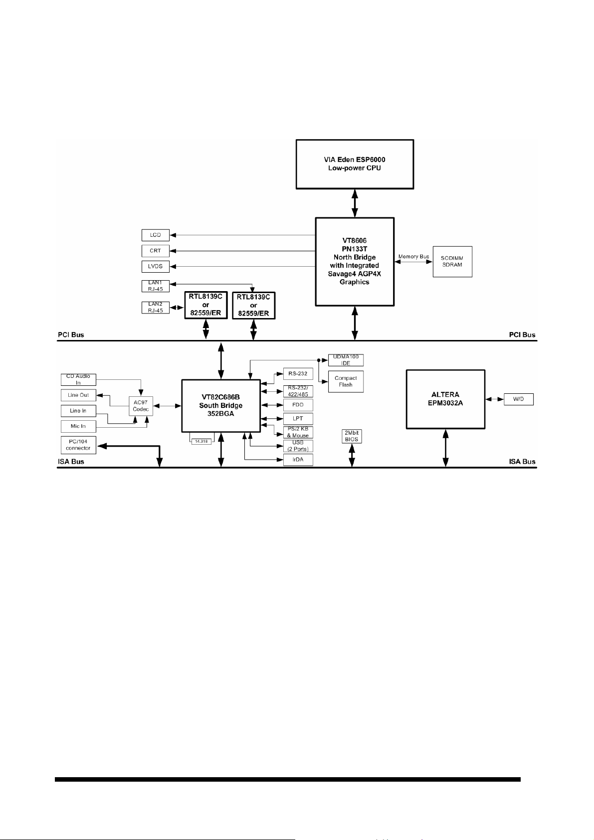
2.3 Architecture Overview
The following block diagram shows the architecture and main components of ECM-3610.
The two key components on board are the VIA VT8606 North Bridge and VT82C686B
super South Bridge. These two devices provide the ISA and PCI bus to which all the major
components are attached.
The following sections provide detail information about the functions provided onboard.
ECM-3610/3610L User’s Manual 5
Page 18

User’s Manual
2.3.1 VIA Eden™ Processor
The VIA C3 processor in Enhanced Ball Grid Array (EBGA) packaging is based upon a
unique internal architecture and is manufactured using advanced 0.15μ or 0.13μ CMOS
technology. The C3 architecture and process technology provide a highly compatible,
high-performance, low-cost, and low-power solution for the desktop PC, notebook, and
Internet Appliance markets. The VIA C3 processor in EBGA is available in several MHz
versions.
When considered individually, the compatibility, function, performance, cost, and power
dissipation of the VIA C3 processor family are all very competitive. Furthermore, the value
added from the advanced EBGA packaging includes remarkable compactness, cost
efficiency and excellent thermal characteristics. The VIA C3 package in EBGA represents
a breakthrough combination for enabling high-value, high-performance, low-power, small
form factor x86-based solutions. When considered as a whole, the VIA C3 processor
family in EBGA offers a peerless level of value.
n Enables flexible & innovative system designs
l Desktop & mobile devices
l Small, low profile form factors
l Fanless implementation for ergonomic silent designs
n Optimizes heat dissipation & power consumption
l Saves energy costs
l Ensures longer battery life in mobile designs
l Enhances reliability, particularly for “always on” designs
2.3.2 VIA VT8606 North Bridge
TwisterT (VT8606) is a high performance, cost-effective and energy efficient SMA chip set
for the implementation of mobile personal computer systems with 66 MHz, 100 MHz and
133 MHz CPU host bus (“Front Side Bus”) frequencies and based on 64-bit Socket-370
(VIA Cyrix III and Intel Celeron and Tualatin) and Slot-1 (Intel Pentium III) super-scalar
processors. TwisterT integrates VIA’s VT82C694T system controller, S3’s Savage4 2D/3D
graphics accelerator and S3’s flat panel interfaces into a single 552 BGA package. The
TwisterT SMA system controller provides superior performance between the CPU, DRAM
and PCI bus with pipelined, burst, and concurrent operation.
TwisterT supports six banks of DRAMs (three memory modules) up to 1.5Gbyte of system
memory with 256Mbit DRAM technology. The DRAM controller supports standard
Synchronous DRAM (SDRAM) and Virtual Channel SDRAM (VC SDRAM), in a flexible
mix / match manner. The Synchronous DRAM interface allows zero wait state bursting
between the DRAM and the data buffers at 100 / 133 MHz. The six banks of DRAM can
be composed of an arbitrary mixture of 1M / 2M / 4M / 8M / 16M / 32MxN DRAMs. The
DRAM controller can run at either the host CPU Front Side Bus frequency (100 / 133 MHz)
or pseudo-synchronous to the CPU FSB frequency (PC100 with the FSB at 133 MHz or
PC133 with the FSB at 100 MHz) with built-in PLL timing control.
6 ECM-3610/3610L User’s Manual
Page 19

ECM-3610/3610L
TwisterT supports a 32-bit 3.3 / 5V system bus (PCI) that is synchronous / pseudosynchronous to the CPU bus. The chip also contains a built-in bus-to-bus bridge to allow
simultaneous concurrent operations on each bus. Five levels (doublewords) of post write
buffers are included to allow for concurrent CPU and PCI operation. For PCI master
operation, forty-eight levels (doublewords) of post write buffers and sixteen levels
(doublewords) of prefetch buffers are included for concurrent PCI bus and DRAM/cache
accesses. The chip also supports enhanced PCI bus commands such as Memory-ReadLine, Memory-Read-Multiple and Memory-Write-Invalid commands to minimize snoop
overhead. In addition, advanced features are supported such as snoop ahead, snoop
filtering, L1 write-back forward to PCI master, and L1 write-back merged with PCI post
writes buffers to minimize
PCI master read latency and DRAM utilization. Delay transaction and read caching
mechanisms are also implemented for further improvement of overall system performance.
TwisterT also integrates S3.’s Savage4 graphics accelerator into a single chip. TwisterT
brings mainstream graphics performance to the Value PC with leading-edge 2D, 3D and
DVD video acceleration into a cost effective package. Based on its capabilities, TwisterT
is an ideal solution for the consumer, corporate mobile users and entry-level professionals.
The industry’s first integrated AGP 4X solution, TwisterT combines AGP 4X performance
with S3’s DX6 texture compression (S3TC) and massive 2Kx2K textures to deliver
unprecedented 3D performance and image quality for the Value PC mobile market.
For sophisticated power management, TwisterT provides independent clock stop control
for the CPU / SDRAM and PCI and Dynamic CKE control for powering down of the
SDRAM. A separate suspend-well plane is implemented for the SDRAM control signals for
Suspend-to-DRAM operation.
2.3.2.1 High-Performance 3D Accelerator
Featuring a new super-pipelined 128-bit engine, TwisterT utilizes a single cycle
architecture that provides high performance along with superior image quality. Several
new features enhance the 3D architecture, including single-pass multitexturing,
anisotropic filtering, and an 8-bit stencil buffer. TwisterT also offers the industry’s only
simultaneous usage of single-pass multitexturing and single-cycle trilinear filtering –
enabling stunning image quality without performance loss. TwisterT further enhances
image quality with true 32-bit color rendering throughout the 3D pipeline to produce more
vivid and realistic images. TwisterT’s advanced triangle setup engine provides industry
leading 3D performance for a realistic user experience in games and other interactive 3D
applications. The 3D engine is optimized for AGP texturing from system memory.
2.3.2.2 128-bit 2D Graphics Engine
TwisterT’s advanced 128-bit 2D graphics engine delivers high-speed 2D acceleration for
productivity applications. Several enhancements have been made to the 2D architecture
to optimize SMA performance and to provide acceleration in all color depths.
ECM-3610/3610L User’s Manual 7
Page 20

User’s Manual
2.3.2.3 DVD Playback and Video Conferencing
TwisterT provides the ideal architecture for high quality MPEG-2 based DVD applications
and video conferencing. For DVD playback, TwisterT’s video accelerator offloads the CPU
by performing the planar to packed format conversion and motion compensation tasks,
while its enhanced scaling algorithm delivers incredible full-screen video playback. For
video conferencing, TwisterT’s multiple video windows enable a cost effective solution.
2.3.2.4 LCD and Flat Panel Monitor Support
TwisterT supports a wide variety of DSTN or TFT panels through a 36-bit interface. This
includes support for VGA, SVGA, XGA, SXGA+, UXGA, and UXGA+ TFT color panels
with 9-bit, 12-bit, 18-bit (both 1 pixel/clock and 2 pixels/clock), and 24-bit interfaces.
Enhanced STN hardware with 256 gray scale supports and advanced frame rate control
to provide up to 16.7 million colors. In addition, the integrated 2-channel LVDS interface
can support another panel. All resolutions are supported up to 1280x1024. The integrated
ZV-Port allows display of video from an external source. An alternative to the 36-bit panel
interface is a 12-bit interface to a TMDS encoder. This interface is Digital Visual Interface
(DVI) 1.0 compliant.
n Defines Integrated Solutions for Value PC Desktops
l High performance SMA North Bridge: Integrated VIA VT82C694X and S3
Savage4 2D/3D graphic accelerator in a single chip
l 64-bit Advanced Memory controller supporting PC133/PC100 SDRAM
n High Performance CPU Interface
l Socket 370, Micro-PGA and Micro FCPGA support for Mobile Intel
Pentium processors
l 133/100/66 MHz CPU Front Side Bus (FSB)
l Built-in Phase Lock Loop circuitry for optimal skew control within and
between clocking regions
l Five outstanding transactions (four In-Order Queue (IOQ) plus one output
latch)
l Dynamic deferred transaction support
n Advanced High - Performance SDRAM Controller
l DRAM interface runs synchronous (100/100, 133/133) mode or pseudo-
synchronous (100/66, 100/133, 133/100) mode with FSB
l Concurrent CPU, AGP, and PCI access
l Supports SDRAM and VCM SDRAM memory types
l Support 3 SODIMMs or 6 banks for up to 1.5 GB of DRAM (256Mb DRAM
technology)
l 64-bit data width
l Supports maximum 8-bank interleave (8 pages open simultaneously); banks
are allocated based on LRU
l SDRAM X-1-1-1-1-1-1-1 back-to-back accesses
8 ECM-3610/3610L User’s Manual
Page 21

n Integrated Savage4 2D/3D/Video Accelerator
l Optimized Shared Memory Architecture (SMA)
l 8/ 16 /32 MB frame buffer using system memory
l Floating point triangle setup engine
l Single cycle 128-bit 3D architecture
l 8M triangles/second setup engine
l 140M pixels/second trilinear fill rate
l Full internal AGP 4x performance
l S3 DX7 texture compression (S3TC)
l Next generation, 128-bit 2D graphics engine
l High quality DVD video playback
l Flat panel monitor support
l 2D/3D resolutions up to 1920x1440 for High resolution CRT support,
n 3D Rendering Features
l Single-pass multiple textures
l Anisotropic filtering
l 8-bit stencil buffer
l 32-bit true color rendering
l Specular lighting and diffuse shading
l Alpha blending modes
l Massive 2K x 2K textures
l MPEG-2 video textures
l Vertex and table fog
l 16 or 24-bit Z-buffering
l Sprite anti-aliasing, reflection mapping, texture morphing, shadows,
procedural textures and atmospheric effects
ECM-3610/3610L
n 2D Hardware Acceleration Features
l ROP3 Ternary Raster Operation BitBLTs
l 8, 16, and 32 bpp mode acceleration
n Motion Video Architecture
l High quality up/down scaler
l Planar to packed format conversion
l Motion compensation for full speed DVD playback
l Hardware subpicture blending and highlights
l Multiple video windows for video conferencing
l Contrast, hue, saturation, brightness and gamma controls
ECM-3610/3610L User’s Manual 9
Page 22

User’s Manual
n Extensive LCD Support
l 36-bit DSTN/TFT flat panel interface with 256 gray shade support
l Integrated 2-channel 110 MHz LVDS interface
l Support for all resolutions up to 1280x1024
l ZV-Port Interface
l Panel power sequencing
l Hardware Suspend/Standby control
n Flat Panel Monitor Support
l 12-bit TFT flat panel interface to TMDS encoders
l Digital Visual Interface (DVI) 1.0 compliant
n Concurrent PCI Bus Controller
l PCI 2.2 compliant, 32-bit 3.3V PCI interface with 5V tolerant inputs
l Supports up to 5 PCI masters
l PCI to system memory data streaming support
l Delay transaction from PCI master accessing DRAM
l Symmetric arbitration between Host/PCI bus for optimized system
performance
n Advanced System Power Management Support
l Dynamic power down of SDRAM (CKE)
l Independent clock stop controls for CPU / SDRAM, AGP, and PCI bus
l PCI and AGP bus clock run and clock generator control
l VTT suspend power plane preserves memory data
l Suspend-to-DRAM and self-refresh power down
l Low-leakage I/O pads
l ACPI 1.0 and PCI Bus Power Management 1.1 compliant
10 ECM-3610/3610L User’s Manual
Page 23

ECM-3610/3610L
2.3.3 VIA VT82C686B South Bridge
The VT82C686B PSIPC (PCI Super-I/O Integrated Peripheral Controller) is a high
integration, high performance, power-efficient, and high compatibility device that supports
Intel and non-Intel based processor to PCI bus bridge functionality to make a complete
Microsoft PC99-compliant PCI/ISA system. In addition to complete ISA extension bus
functionality, the VT82C686B includes standard intelligent peripheral controllers:
n Master mode enhanced IDE controller with dual channel DMA engine and
interlaced dual channel commands. Dedicated FIFO coupled with scatter and
gather master mode operation allows high performance transfers between PCI
and IDE devices. In addition to standard PIO and DMA mode operation. The
VT82C686B also supports the UltraDMA-33, UltraDMA-66, and UltraDMA-100
(ATA-100) standards. The IDE controller is SFF-8038I v1.0 and Microsoft
Windows-family compliant.
n Universal Serial Bus controller that is USB v1.1 and Universal HCI v1.1
compliant. The VT82C686B includes the root hub with four function ports with
integrated physical layer transceivers. The USB controller allows hot plug and
play and isochronous peripherals to be inserted into the system with universal
driver support. The controller also implements legacy keyboard and mouse
support so that legacy software can run transparently in a non-USB-aware
operating system environment.
n Keyboard controller with PS2 mouse support.
n Real Time Clock with 256 byte extended CMOS. In addition to the standard ISA
RTC functionality, the integrated RTC also includes the date alarm, century field,
and other enhancements for compatibility with the ACPI standard.
n Notebook-class power management functionality compliant with ACPI and legacy
APM requirements. Multiple sleep states (power-on suspend, suspend-to-DRAM,
and suspend-to-Disk) are supported with hardware automatic wake-up.
Additional functionality includes event monitoring, CPU clock throttling and stop
(Intel processor protocol), PCI bus clock stop control, modular power, clock and
leakage control, hardware-based and software-based event handling, general
purpose I/O, chip select and external SMI.
n Hardware monitoring subsystem for managing system / motherboard voltage
levels, temperatures, and fan speeds
n Full System Management Bus (SMBus) interface.
n Two 16550-compatible serial I/O ports with infrared communications port option
on the second port.
ECM-3610/3610L User’s Manual 11
Page 24

User’s Manual
n Integrated PCI-mastering dual full-duplex direct-sound AC97-link-compatible
sound system. Hardware soundblaster-pro and hardware-assisted FM blocks are
included for Windows DOS box and real-mode DOS compatibility. Loopback
capability is also implemented for directing mixed audio streams into USB and
1394 speakers for high quality digital audio.
n Two game ports and one MIDI port
n ECP/EPP-capable parallel port
n Standard floppy disk drive interface
n Distributed DMA capability for support of ISA legacy DMA over the PCI bus.
Serial IRQ is also supported for docking and non-docking applications.
n Plug and Play controller that allows complete steerability of all PCI interrupts and
internal interrupts / DMA channels to any interrupt channel. One additional
steerable interrupt channel is provided to allow plug and play and
reconfigurability of on-board peripherals for Windows family compliance.
n Internal I/O APIC (Advanced Programmable Interrupt Controller)
2.3.3.1 IDE Interface (Bus Master Capability and Synchronous DMA Mode)
Master mode enhanced IDE controller with dual channel DMA engine and interlaced dual
channel commands. Dedicated FIFO coupled with scatter and gather master mode
operation allows high performance transfers between PCI and IDE devices. In addition to
standard PIO and DMA mode operation. The VT82C686B also supports the UltraDMA-33,
UltraDMA-66, and UltraDMA-100 (ATA-100) standards. The IDE controller is SFF-8038I
v1.0 and Microsoft Windows-family compliant.
2.3.3.2 USB
Universal Serial Bus controller that is USB v1.1 and Universal HCI v1.1 compliant. The
VT82C686B includes the root hub with four function ports with integrated physical layer
transceivers. The USB controller allows hot plug and play and isochronous peripherals to
be inserted into the system with universal driver support. The controller also implements
legacy keyboard and mouse support so that legacy software can run transparently in a
non-USB-aware operating system environment.
12 ECM-3610/3610L User’s Manual
Page 25

ECM-3610/3610L
2.3.4 Realtek RTL8139C Ethernet Controller
The Ethernet interfaces are based on two Realtek RTL8139C Ethernet controllers which
support both 100Mbit as well as 10Mbit Base-T interface.
The Ethernet controllers are attached to the PCI bus and use PCI bus mastering for data
transfer. The CPU is thereby not loaded during the actual data transfer.
The Realtek RTL8139C is a highly integrated and cost-effective single-chip Fast Ethernet
controller that provides 32-bit performance, PCI bus master capability, and full compliance
with IEEE 802.3u 100Base-T specifications and IEEE 802.3x Full Duplex Flow Control. It
also supports Advanced Configuration Power management Interface (ACPI), PCI power
management for modern operating systems that is capable of Operating System Directed
Power Management (OSPM) to achieve the most efficient power management.
2.3.5 Intel 82559ER Ethernet Controller (Optional)
The 82559ER is part of Intel's second generation family of fully integrated 10BASET/100BASE-TX LAN solutions. The 82559ER consists of both the Media Access
Controller (MAC) and the physical layer (PHY) combined into a single component solution.
82559 family members build on the basic functionality of the 82558 and contain power
management enhancements.
The 82559ER is a 32-bit PCI controller that features enhanced scatter-gather bus
mastering capabilities which enables the 82559ER to perform high-speed data transfers
over the PCI bus. The 82559ER bus master capabilities enable the component to process
high-level commands and perform multiple operations, thereby off-loading communication
tasks from the system CPU. Two large transmit and receive FIFOs of 3 Kbytes each help
prevent data underruns and overruns, allowing the 82559ER to transmit data with
minimum interframe spacing (IFS).
The 82559ER can operate in either full duplex or half duplex mode. In full duplex mode
the 82559ER adheres to the IEEE 802.3x Flow Control specification. Half duplex
performance is enhanced by a proprietary collision reduction mechanism.
The 82559ER includes a simple PHY interface to the wire transformer at rates of 10BASET and 100BASE-TX, and Auto-Negotiation capability for speed, duplex, and flow control.
These features and others reduce cost, real estate, and design complexity.
The 82559ER also includes an interface to a serial (4-pin) EEPROM and a parallel
interface to a 128 Kbyte Flash memory. The EEPROM provides power-on initialization for
hardware and software configuration parameters
ECM-3610/3610L User’s Manual 13
Page 26

User’s Manual
2.3.6 Compact Flash Interface
A Compact Flash type II connector is connected to the secondary IDE controller. The
Compact Flash storage card is IDE compatible. It is an ideal replacement for standard IDE
hard drives. The solid-state design offers no seek errors even under extreme shock and
vibration conditions. The Compact Flash storage card is extremely small and highly
suitable for rugged environments, thus providing an excellent solution for mobile
applications with space limitations. It is fully compatible with all consumer applications
designed for data storage PC card, PDA, and Smart Cellular Phones, allowing simple use
for the end user. The Compact Flash storage card is O/S independent, thus offering an
optimal solution for embedded systems operating in non-standard computing
environments. The Compact Flash storage card is IDE compatible and offers various
capacities.
14 ECM-3610/3610L User’s Manual
Page 27

ECM-3610/3610L
3. Hardware Configuration
This chapter explains you the instructions of how to setup your system.
3.1 Installation Procedure
1. Turn off the power supply.
2. Insert the SODIMM module (be careful with the orientation and refer to chapter 3.3 for
details)
3. Connect all external cables for hard disk, floppy, keyboard, mouse, USB etc. except for
flat panel. A CRT monitor must be connected in order to change CMOS settings to
support flat panel.
4. Connect power supply to the board.
5. Turn on the power.
6. Enter the BIOS setup by pressing the delete key during boot up. Use the “LOAD BIOS
DEFAULTS” feature. The Integrated Peripheral Setup and the Standard CMOS
Setup Window must be entered and configured correctly to match the particular
system configuration.
7. If TFT panel display is to be used, make sure the panel voltage is correctly set before
connecting the display cable and turning on the power.
3.2 Safety Precautions
3.2.1 Warning!
Always completely disconnect the power cord from your chassis or power
cable from your board whenever you work with the hardware. Do not make
connections while the power is on. Sensitive electronic components can
be damaged by sudden power surges. Only experienced electronics
personnel should open the PC chassis.
3.2.2 Caution!
Always ground yourself to remove any static charge before touching the
board. Modern electronic devices are very sensitive to static electric
charges. As a safety precaution, use a grounding wrist strap at all times.
Place all electronic components in a static-dissipative surface or staticshielded bag when they are not in the chassis.
ECM-3610/3610L User’s Manual 15
Page 28

User’s Manual
3.3 Installing DRAM (SODIMMs)
3.3.1 System Memory
The reverse side of the ECM-3610 contains a socket for 144-pin dual inline memory
module (SODIMM). The socket uses 3.3 V unbuffered synchronous DRAM (SDRAM).
SODIMM module is available in capacities of 32, 64, 128, 128 or 512 MB. The socket can
be filled in the SODIMM of any size, giving your ECM-3610 single board between 32 and
512 MB of memory.
3.3.2 Memory Installation Procedures
Press the SODIMM module right down into the socket, until you hear a click. This is when
the two handles have automatically locked the memory module into the correct position of
the SODIMM socket. (See Figure below) To take away the memory module, just push both
handles outward, and the memory module will be ejected by the mechanism in the socket.
16 ECM-3610/3610L User’s Manual
Page 29
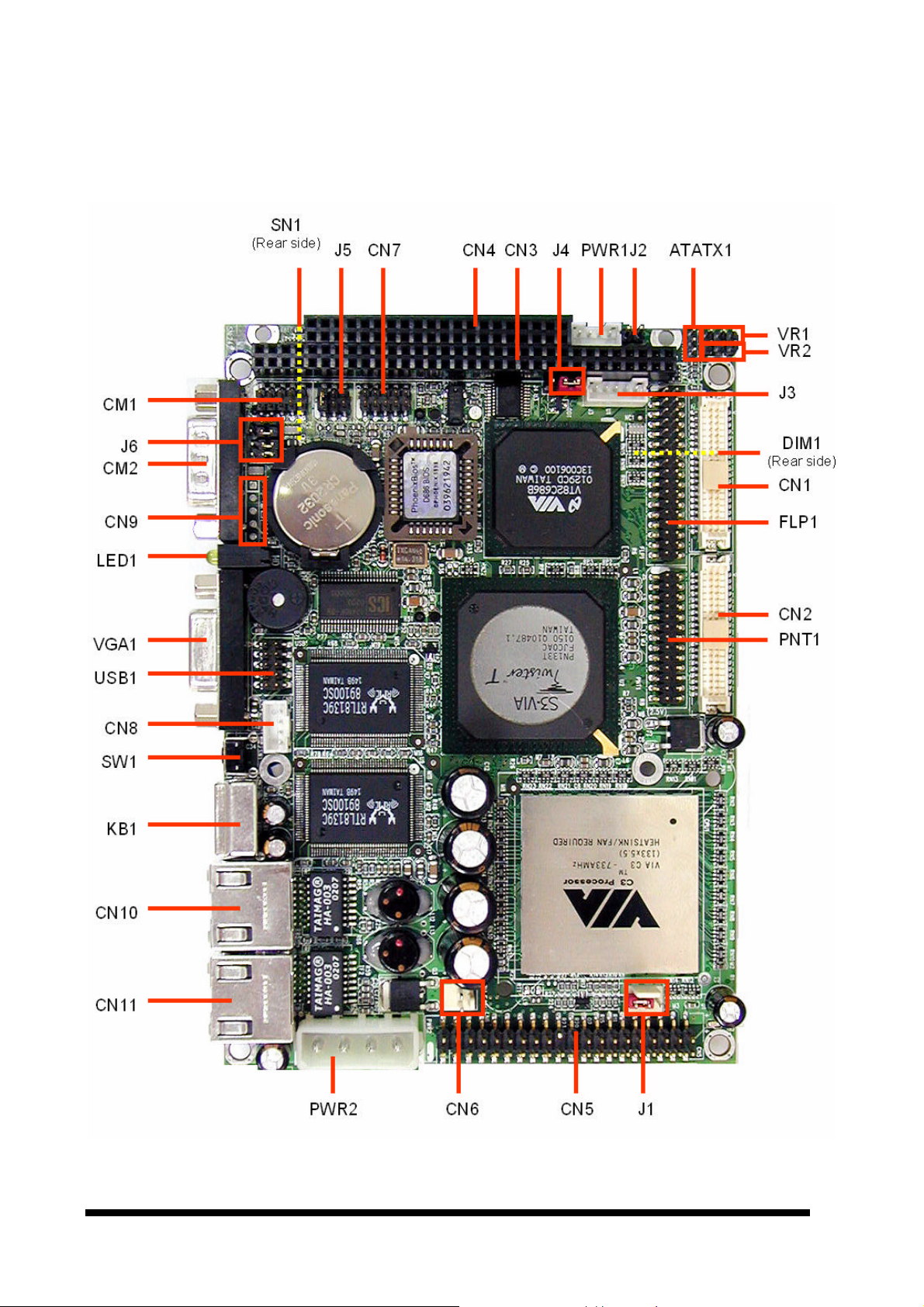
3.4 Jumper & Connector
3.4.1 Jumper & Connector Layout
ECM-3610/3610L
ECM-3610/3610L User’s Manual 17
Page 30

User’s Manual
3.5 Jumper and Connector List
Connectors on the board are linked to external devices such as hard disk drives, a
keyboard, or floppy drives. In addition, the board has a number of jumpers that
allow you to configure your system to suit your application.
The following tables list the function of each of the board's jumpers and connectors.
Jumpers
Label Function Note
J4
J5, J6
ATATX1
Clear CMOS 3 x 1 header, pitch 2.54mm
COM2 RS-232/422/485 select 3 x 2 header, pitch 2.0mm
4 x 3 header, pitch 2.0mm (J6)
AT / ATX power select 3 x 1 header, pitch 2.0mm
18 ECM-3610/3610L User’s Manual
Page 31

ECM-3610/3610L
Connectors
Label Function Note
CM1
CM2
CN1
CN2
CN3, CN4
CN5
CN6
CN7
CN8
CN9
CN10 (LAN1)
CN11 (LAN2)
DIM1
FLP1
Serial port 2 connector 5 x 2 header, pitch 2.0mm
Serial port 1 connector DB-9 male connector
Secondary LCD panel connector HIROSE DF13-40DP-1.25V
Primary LCD panel connector HIROSE DF13-40DP-1.25V
PC/104 connector
IDE connector 20 x 2 header, pitch 2.54mm
CPU fan connector 2 x 1 wafer, pitch 2.54mm
Audio connector 5 x 2 header, pitch 2.0mm
CD-ROM audio input connector 4 x 1 wafer, pitch 2.0mm
IrDA connector 5 x 1 header, pitch 2.0mm
10/100Base-Tx Ethernet 1 connector RJ-45
10/100Base-Tx Ethernet 2 connector RJ-45 (ECM-3610 only)
144-pin SODIMM socket (Real side)
Floppy connector 17 x 2 header, pitch 2.0mm
J1
J2
J3
KB1
PNT1
PWR1
PWR2
SN1
SW1
USB1
VGA1
VR1
VR2
ATX Power connector 3 x 1 wafer, pitch 2.54mm
ATX Soft-power bottom 2 x 1 header, pitch 2.54mm
LCD inverter connector 5 x 1 wafer, pitch 2.0mm
Keyboard and PS/2 mouse connector 6-pin mini DIN
Parallel port connector 13 x 2 header, pitch 2.0mm
Auxiliary power connector 4 x 1 wafer, pitch 2.0mm
Power connector Molex A-8981-04V5
Compact Flash connector (Real side)
Reset button
USB connector 5 x 2 header, pitch 2.0mm
CRT connector DB-15 female connector
LCD backlight brightness adjustment
connector
STN LCD contrast adjustment connector 3 x 1 header, pitch 2.54mm
3 x 1 header, pitch 2.54mm
ECM-3610/3610L User’s Manual 19
Page 32
User’s Manual
2
2
3.6 Setting Jumpers
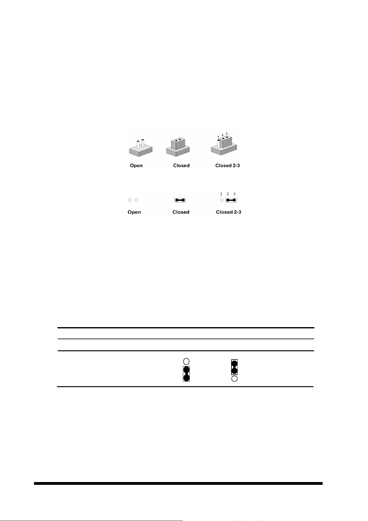
You can configure your board to match the needs of your application by setting jumpers. A
jumper is the simplest kind of electric switch.
It consists of two metal pins and a small metal clip (often protected by a plastic cover) that
slides over the pins to connect them. To “close” a jumper you connect the pins with the
clip. To “open” a jumper you remove the clip. Sometimes a jumper will have three pins,
labeled 1, 2, and 3. In this case, you would connect either two pins.
The jumper settings are schematically depicted in this manual as follows:
A pair of needle-nose pliers may be helpful when working with jumpers.
If you have any doubts about the best hardware configuration for your application, contact
your local distributor or sales representative before you make any changes.
3.6.1 Clear CMOS (J4)
You can use J4 to clear the CMOS data if necessary. To reset the CMOS data, set
J4 to 2-3 closed for just a few seconds, and then move the jumper back to 1-2
closed.
Clear CMOS (J4)
Clear CMOS Protect*
1
1
J4
3
3
* default
20 ECM-3610/3610L User’s Manual
Page 33
2
2
6 4 2
6 4 2
6 4 2
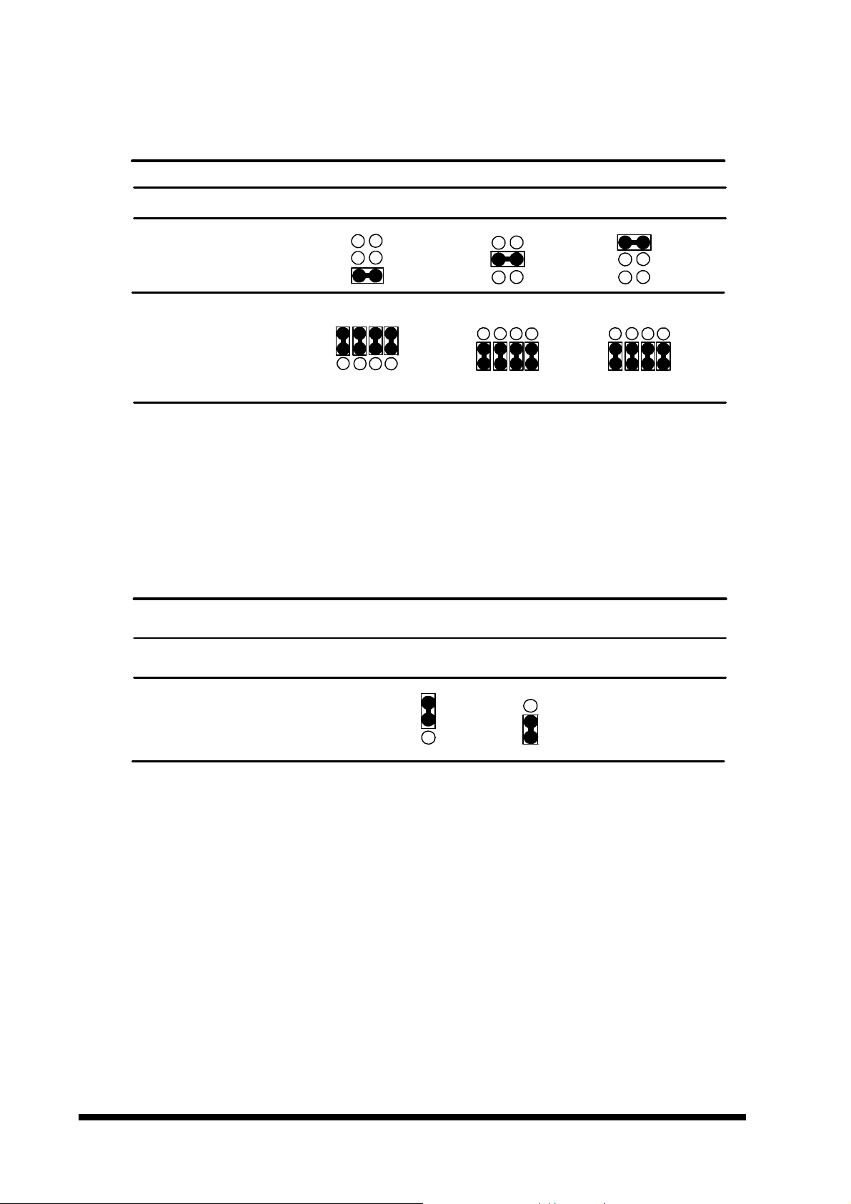
3.6.2 COM2 RS-232/422/485 Select (J5, J6)
COM2 RS-232/422/485 Select (J5, J6)
J5
RS-232* RS-422 RS-485
1 4 7 10
5
3
1
1 4 7 10
5
3
1
ECM-3610/3610L
5
3
1
1 4 7 10
J6
3 6 9 12
* default
3.6.3 AT/ATX Power Select (ATATX1)
You can use ATATX1 to select the power supply type. To use the AT power supply,
set ATATX1 to 1-2 closed. Set ATATX1 to 1-2 closed (and J1 to 2-3 closed), if ATX
power supply is to be used.
AT/ATX Power Select (ATATX1)
AT P/S* ATX P/S
ATATX1
* default
Note:
Set J1 to 2-3 closed, if AT power supply is to be used.
3 6 9 12
3 6 9 12
1
3
1
3
ECM-3610/3610L User’s Manual 21
Page 34
User’s Manual
board UART
3.7 Connector Definitions
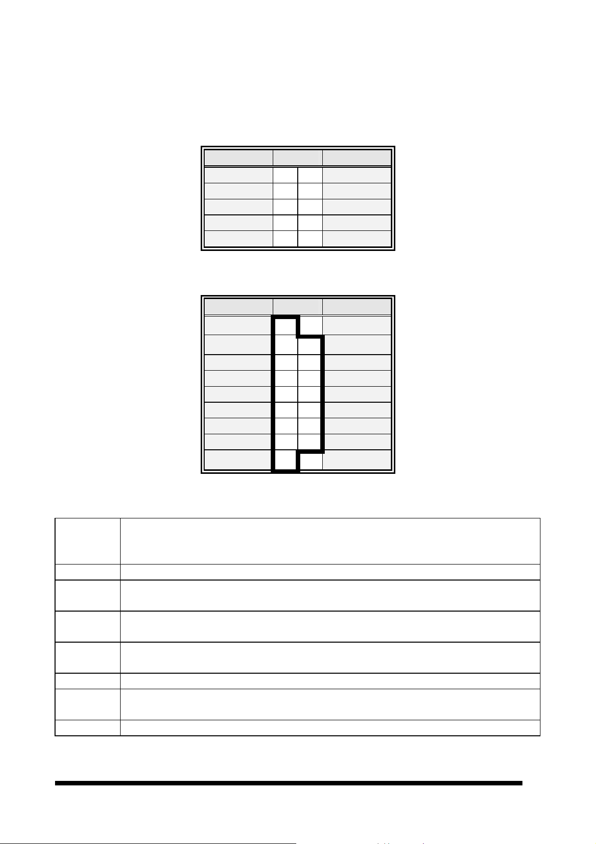
3.7.1 Pin Header Serial Port 2 Connector in RS-232 Mode (CM1)
Signal PIN Signal
DCD 1 2 RxD
TxD 3 4 DTR
GND 5 6 DSR
RTS 7 8 CTS
RI 9 10
NC
3.7.2 Serial Port 2 with External DB9 Connector (CM1)
Signal PIN Signal
GND 5
9
DTR 4
8
TxD 3
7
RxD 2
6
DCD 1
RI
CTS
RTS
DSR
3.7.3 Signal Description – Serial Port 2 – COM2 in RS-232 Mode (CM1)
TxD Serial output. This signal sends serial data to the communication link. The signal is set to a
marking state on hardware reset when the transmitter is empty or when loop mode operation
is initiated.
RxD Serial input. This signal receives serial data from the communication link.
DTR Data Terminal Ready. This signal indicates to the modem or data set that the on-
is ready to establish a communication link.
DSR Data Set Ready. This signal indicates that the modem or data set is ready to establish a
communication link.
RTS Request To Send. This signal indicates to the modem or data set that the on-board UART is
ready to exchange data.
CTS Clear To Send. This signal indicates that the modem or data set is ready to exchange data.
DCD Data Carrier Detect. This signal indicates that the modem or data set has detected the data
carrier.
RI Ring Indicator. This signal indicates that the modem has received a telephone ringing signal.
22 ECM-3610/3610L User’s Manual
Page 35
ECM-3610/3610L
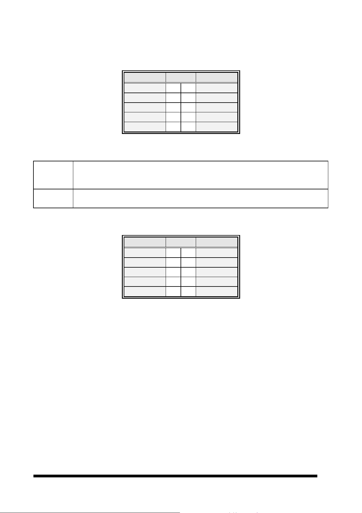
3.7.4 Pin Header Serial Port 2 Connector in RS-422 Mode (CM1)
Signal PIN Signal
Tx- 1 2 Rx+
Tx+ 3 4 Rx-
NC 5 6 NC
NC 7 8 NC
NC 9 10
NC
3.7.5 Signal Description – Serial Port 2 – COM2 in RS-422 Mode (CM1)
Tx +/- Serial output. This differential signal pair sends serial data to the communication link. Data is
transferred from Serial Port 2 Transmit Buffer Register to the communication link, if the RTS
register of the Serial Port 2 is set to LOW.
Rx +/- Serial input. This differential signal pair receives serial data from the communication link.
Received data is available in Serial Port 2 Receiver Buffer Register.
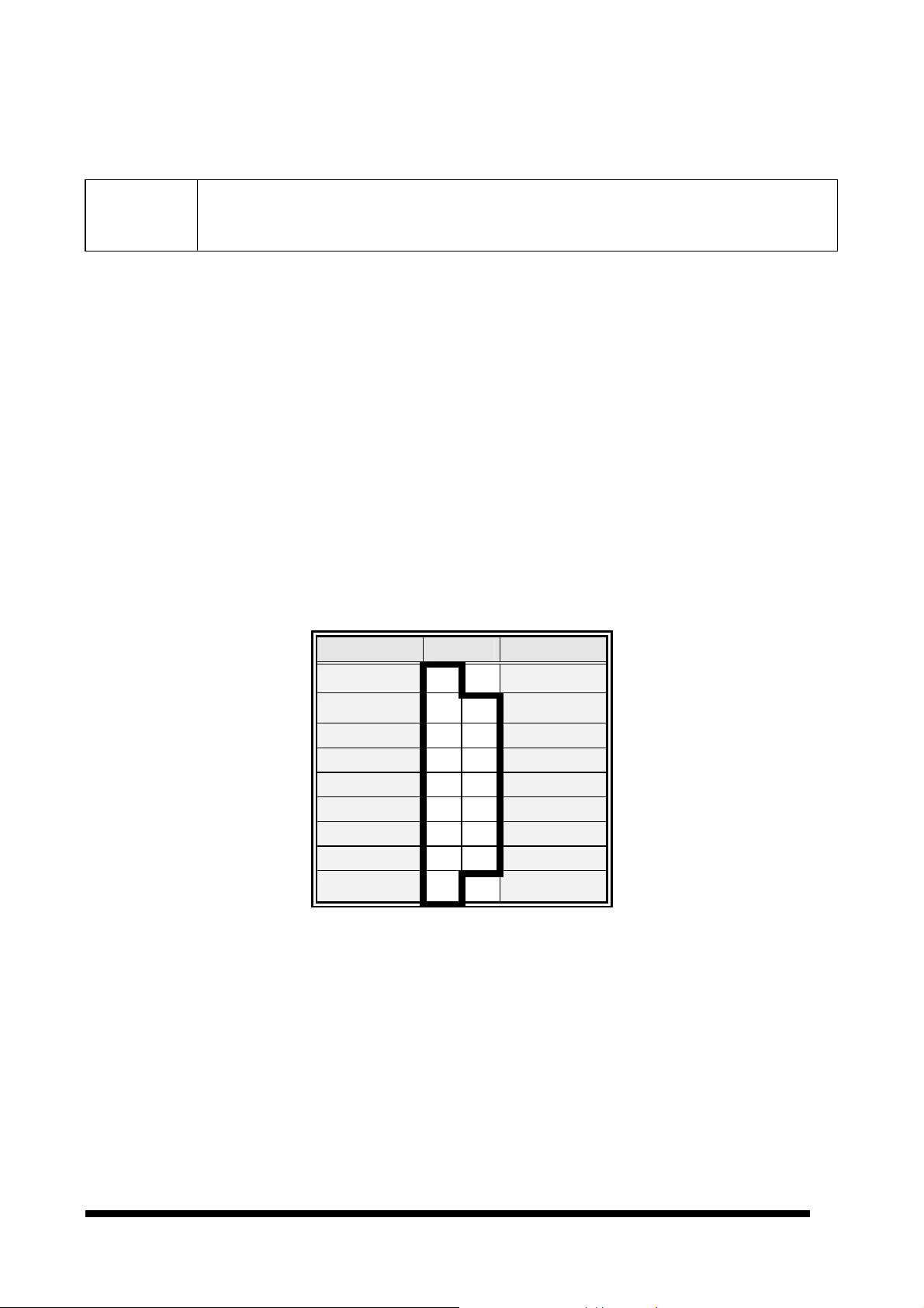
3.7.6 Pin Header Serial Port 2 Connector in RS-485 Mode (CM1)
Signal PIN Signal
DATA- 1 2 NC
DATA+ 3 4 NC
NC 5 6 NC
NC 7 8 NC
NC 9 10
NC
ECM-3610/3610L User’s Manual 23
Page 36
User’s Manual
3.7.7 Signal Description – Serial Port 2 – COM2 in RS-485 Mode (CM1)
DATA +/- This differential signal pair sends and receives serial data to the communication link. The
mode of this differential signal pair is controlled through the RTS register of Serial Port 2.
Set the RTS register of the Serial Port 2 to LOW for transmitting, HIGH for receiving.
Warning: Do not select a mode different from the one used by the connected peripheral,
as this may damage CPU board and/or peripheral.
The transmitter drivers in the port are short circuit protected by a thermal
protection circuit. The circuit disables the drivers when the die temperature
reaches 150 °C.
RS-422 mode is typically used in point to point communication. Data and
control signal pairs should be terminated in the receiver end with a resistor
matching the cable impedance (typ. 100-120 Ω). The resistors could be placed
in the connector housing.
RS-485 mode is typically used in multi drop applications, where more than 2
units are communicating. The data and control signal pairs should be
terminated in each end of the communication line with a resistor matching the
cable impedance (typical 100-120 Ω). Stubs to substations should be avoided.
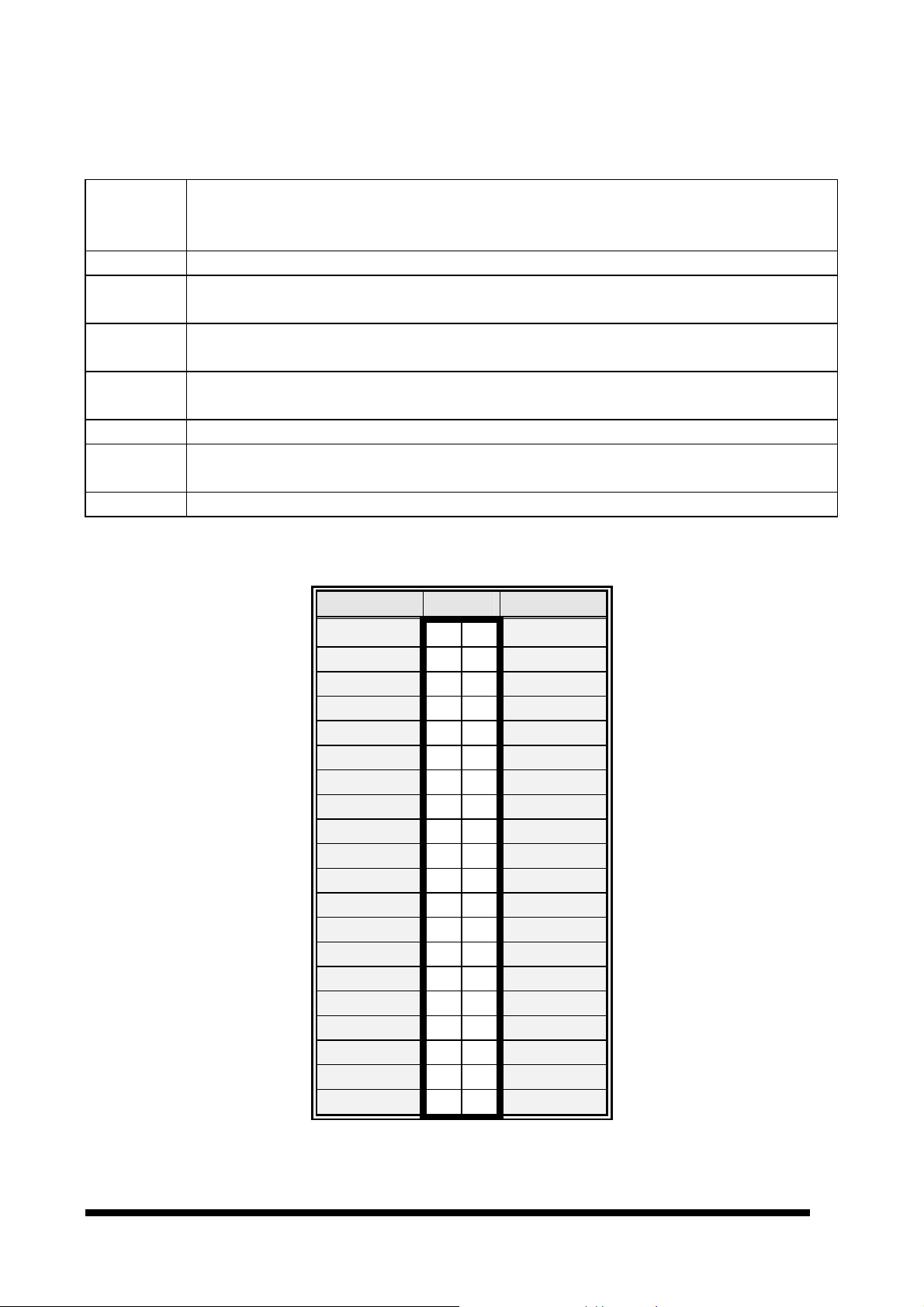
3.7.8 Serial Port 1 with External DB9 Connector (CM2)
Signal PIN Signal
GND 5
9
DTR 4
8
TxD 3
7
RxD 2
6
DCD 1
RI
CTS
RTS
DSR
24 ECM-3610/3610L User’s Manual
Page 37
ECM-3610/3610L
UART
3.7.9 Signal Description – Serial Port 1 – COM1 in RS-232 Mode (CM2)
TxD Serial output. This signal sends serial data to the communication link. The signal is set to a
marking state on hardware reset when the transmitter is empty or when loop mode operation
is initiated.
RxD Serial input. This signal receives serial data from the communication link.
DTR Data Terminal Ready. This signal indicates to the modem or data set that the on-board
is ready to establish a communication link.
DSR Data Set Ready. This signal indicates that the modem or data set is ready to establish a
communication link.
RTS Request To Send. This signal indicates to the modem or data set that the on-board UART is
ready to exchange data.
CTS Clear To Send. This signal indicates that the modem or data set is ready to exchange data.
DCD Data Carrier Detect. This signal indicates that the modem or data set has detected the data
carrier.
RI Ring Indicator. This signal indicates that the modem has received a telephone ringing signal.
3.7.10 Secondary LCD Panel Connector (CN1)
Signal PIN Signal
5V 2 1
GND 4 3
3.3V 6 5
GND 8 7
P25 10 9
P27 12 11
P29 14 13
P31 16 15
P33 18 17
P35 20 19
GND 22 21
Y2M 24 23
Z1M 26 25
ZCM 28 27
Z0M 30 29
YCM 32 31
GND 34 33
Y0M 36 35
Z2M 38 37
Y1M 40 39
5V
GND
3.3V
Vcon
P24
P26
P28
P30
P32
P34
GND
Y2P
Z1P
ZCP
Z0P
YCP
GND
Y0P
Z2P
Y1P
ECM-3610/3610L User’s Manual 25
Page 38
User’s Manual
Multipurpose signal, function depends on panel type. May be used as AC drive control
on/off sequencing. A high level may turn
3.7.11 Primary LCD Panel Connector (CN2)
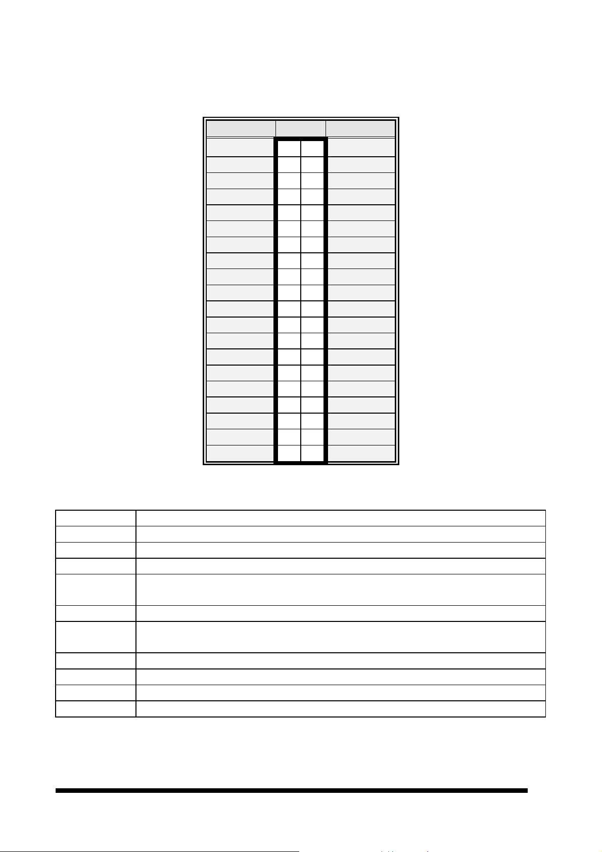
Signal PIN Signal
5V 2 1
GND 4 3
3.3V 6 5
GND 8 7
P1 10 9
P3 12 11
P5 14 13
P7 16 15
P9 18 17
P11 20 19
P13 22 21
P15 24 23
P17 26 25
P19 28 27
P21 30 29
P23 32 31
GND 34 33
FLM 36 35
LP 38 37
ENVEE 40 39
5V
GND
3.3V
Vcon
P0
P2
P4
P6
P8
P10
P12
P14
P16
P18
P20
P22
GND
SHFCLK
M
ENBKL
3.7.12 Signal Description – Primary & Secondary LCD Panel Connector (CN2, CN1)
P [35:0] Flat Panel Data Bit 35 to Bit 0 for panel implementation.
SHFCLK Shift Clock. Pixel clock for flat panel data
LP Latch Pulse. Flat panel equivalent of HSYNC (horizontal synchronization)
FLM First Line Marker. Flat panel equivalent of VSYNC (vertical synchronization)
M
ENBKL Enable backlight signal. This signal is controlled as a part of the panel power sequencing
ENVEE
Y[2:0]P, Z[2:0]P
Y[2:0]M, Z[2:0]M
YCP, ZCP
YCM, ZCM
signal or as BLANK# or Display Enable signal
Enable VEE. Signal to control the panel poweron the VEE (LCD bias voltage) supply to the panel
nd
1st & 2
1st & 2
1st & 2
1st & 2
Channel Positive LVDS differentiaI data output
nd
Channel Negative LVDS differential data output
nd
Channel Positive LVDS differential clock output
nd
Channel Negative LVDS differential clock output
26 ECM-3610/3610L User’s Manual
Page 39

3.7.13 Signal Configuration – DSTN Displays
STN DSTN
ECM-3610/3610L
Pin name
P35
P34
P33
P32 UG2 UG2
P31
P30 UR2 UR2
P29 UB3
P28 UB1 UB1
P27
P26 UG1 UG1
P25 UG3
P24 UR1 UR1 UR1
P23 B7 UR0 UR0
P22 G7 UB0 UB0 UB0 UR1 UR1
P21 R7 UR2 UR2
P20 B6 UG0 UG0 UG0 UR3
P19 G6 UR3 LR0 LR0
P18 R6 UR0 UR0 UR0 LR1 LR1
P17 B5 LR2 LR2
P16 G5 LR3
P15 R5 R5 UG0 UG0
P14 B4 B4 LG2 LG2 UG1 UG1
P13 G4 G4 LB3 UG2 UG2
P12 R4 R4 LR2 LR2 UG3
P11 B3 B3 LG0 LG0
P10 G3 G3 LB1 LB1 LG1 LG1
P9 R3 R3 LG2 LG2
P8 B2 B2 LG1 LG1 LG3
P7 G2 G2 G2 LG3 UB0 UB0
P6 R2 R2 R2 LR1 LR1 LR1 UB1 UB1
P5 B1 B1 B1 UB2
P4 G1 G1 G1 LB0 LB0 LB0 UB3
P3 R1 R1 R1 LB0 LB0
P2 B0 B0 B0 LG0 LG0 LG0 LB1 LB1
P1 G0 G0 G0 LR3 LB2
P0 R0 R0 R0 LR0 LR0 LR0 LB3
8-bit 16-bit 24-bit 8-bit 16-bit 24-bit 16-bit 24-bit
ECM-3610/3610L User’s Manual 27
Page 40

User’s Manual
3.7.14 Signal Configuration – TFT Displays
TFT
Pin name 9-bit 9-bit x 2
P35 B12 B13 B14 B15
P34 B2 B02 B3 B03 B4 B04 B14
P33 B11 B12 B13 B13
P32 B1 B01 B2 B02 B3 B03 B12
P31 B10 B11 B12 B11
P30 B0 B00 B1 B01 B2 B02 B10
P29 B10 B11 G15
P28 B0 B00 B1 B01 G14
P27 B10 G13
P26 B0 B00 G12
P25 G11
P24 G10
P23 G12 G13 G14 R5 R05 R7
P22 G2 G02 G3 G03 G4 G04 R4 R04 R6
P21 G11 G12 G13 R3 R03 R5
P20 G1 G01 G2 G02 G3 G03 R2 R02 R4
P19 G10 G11 G12 R1 R01 R3
P18 G0 G00 G1 G01 G2 G02 R0 R00 R2
P17 G10 G11 R11 R1
P16 G0 G00 G1 G01 R10 R0
P15 G10 G5 G05 G7
P14 G0 G00 G4 G04 G6
P13 G3 G03 G5
P12 G2 G02 G4
P11 R12 R13 R14 G1 G01 G3
P10 R2 R02 R3 R03 R4 R04 G0 G00 G2
P9 R11 R12 R13 R13 G1
P8 R1 R01 R2 R02 R3 R03 R12 G0
P7 R10 R11 R12 B5 B05 B7
P6 R0 R00 R1 R01 R2 R02 B4 B04 B6
P5 R10 R11 B3 B03 B5
P4 R0 R00 R1 R01 B2 B02 B4
P3 R10 B1 B01 B3
P2 R0 R00 B0 B00 B2
P1 R15 B1
P0 R14 B0
12-bit 12-bit x 2 15-bit 15-bit x 2 18-bit 18-bit x 2 24-bit
Note:
The principle of attachment of TFT panels is that the bits for red, green, and blue
use the most significant bits and skip the least significant bits if the display
interface width of the TFT panel is insufficient.
28 ECM-3610/3610L User’s Manual
Page 41
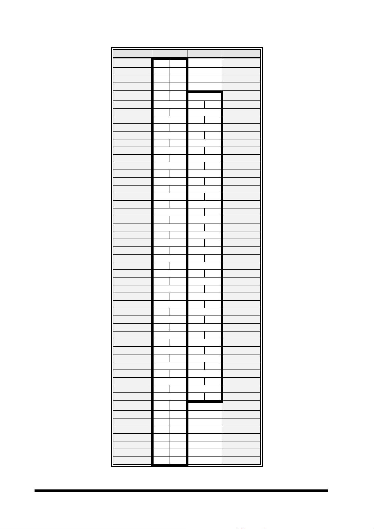
3.7.15 PC/104 Connector (CN3, CN4)
Signal PIN PIN Signal
GND B32 A32
GND B31 A31
OSC B30 A30
VCC B29 A29
BALE B28 A28
NC C19 D19
TC B27 A27
SD15 C18 D18
DACK2# B26 A26
SD14 C17 D17 MASTER#
IRQ3 B25 A25
SD13 C16 D16
IRQ4 B24 A24
SD12 C15 D15
IRQ5 B23 A23
SD11 C14 D14 DACK7#
IRQ6 B22 A22
SD10 C13 D13
IRQ7 B21 A21
SD9 C12 D12 DACK6#
SYSCLK B20 A20
SD8 C11 D11
REFRESH# B19 A19
SMEMW#
DRQ1 B18 A18
SMEMR#
DACK1# B17 A17
LA17 C8 D8 DACK0#
DRQ3 B16 A16
LA18 C7 D7
DACK3# B15 A15
LA19 C6 D6
IOR# B14 A14
LA20 C5 D5
IOW# B13 A13
LA21 C4 D4
SMEMR# B12 A12
LA22 C3 D3
SMEMW# B11 A11
LA23 C2 D2 IOCS16#
GND B10 A10
SBHE# C1 D1 MEMCS16#
+ 12 V B9 A9
GND C0 D0
OWS# B8 A8
- 12 V B7 A7
DRQ2 B6 A6
- 5 V B5 A5
IRQ9 B4 A4
VCC B3 A3
RESETDRV B2 A2
GND B1 A1
GND
SA0
SA1
SA2
SA3
GND
SA4
GND
SA5
SA6
VCC
SA7
DRQ7
SA8
SA9
DRQ6
SA10
SA11
DRQ5
SA12
C10 D10 DACK5#
SA13
C9 D9
SA14
SA15
SA16
SA17
SA18
SA19
AEN
IOCHRDY
SD0
SD1
SD2
SD3
SD4
SD5
SD6
SD7
IOCHCHK#
DRQ0
IRQ14
IRQ15
IRQ12
IRQ11
IRQ10
GND
ECM-3610/3610L
ECM-3610/3610L User’s Manual 29
Page 42
User’s Manual
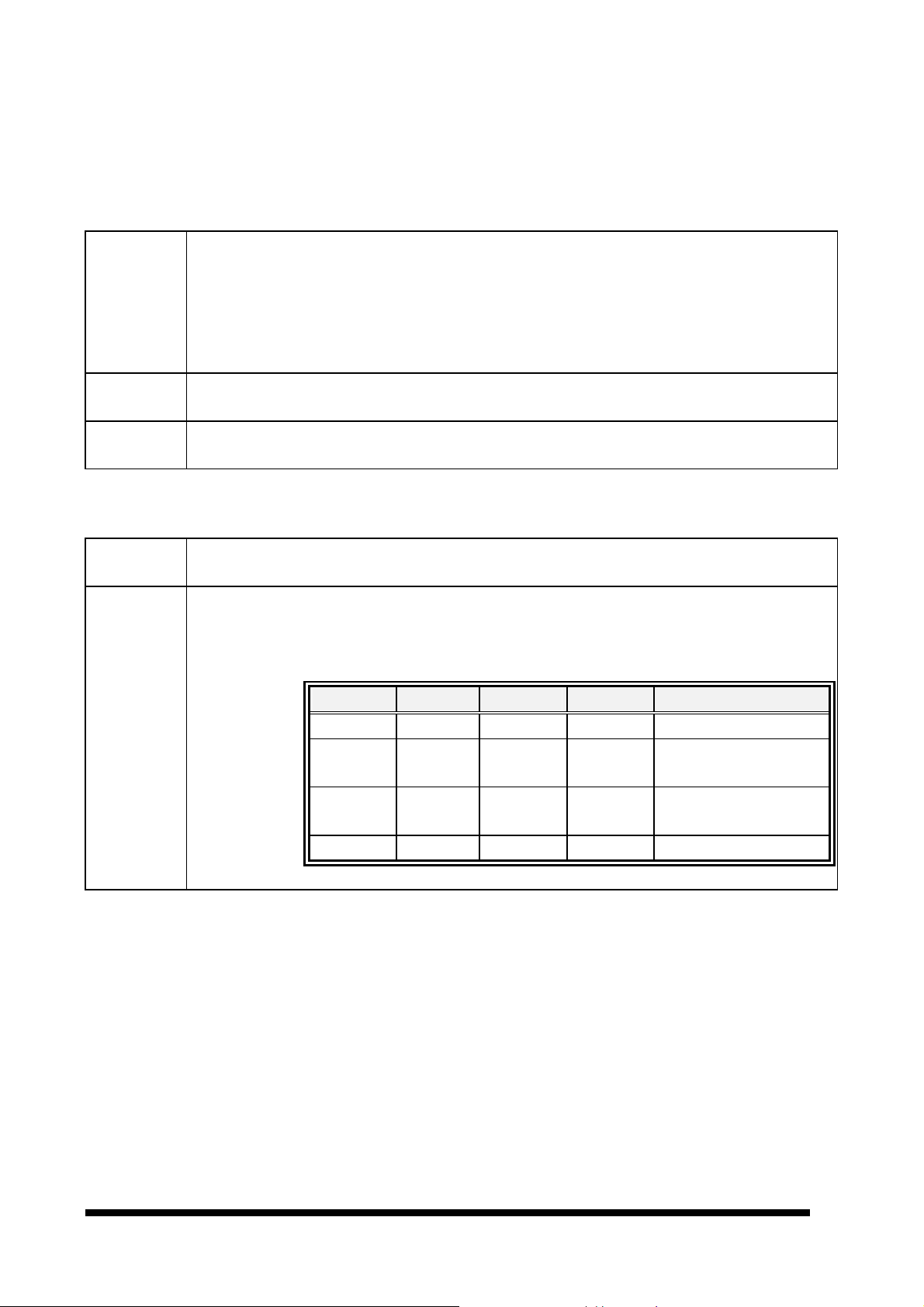
3.7.16 Signal Description – PC/104 Connector (CN3, CN4)
3.7.16.1 Address
LA [23:17] The address signals LA [23:17] define the selection of a 128KB section of memory space
within the 16MB address range of the 16-bit data bus. These signals are active high. The
validity of the MEMCS16# depends on these signals only. These address lines are presented
to the system with tri-state drivers. The permanent master drives these lines except when an
alternate master cycle occurs; in this case, the temporary master drives these lines. The LA
signals are not defined for I/O accesses.
SA [19:0] System address. Address lines for the first one Megabyte of memory. SA [9:0] used for I/O
addresses. SA0 is the least significant bit
SBHE# This signal is an active low signal, that indicates that a byte is being transferred on the upper
byte (SD [15:8]) of the 16 bit bus. All bus masters will drive this line with a tri-state driver.
3.7.16.2 Data
SD [15:8] These signals are defined for the high order byte of the 16-bit data bus. Memory or I/O
transfers on this part of the bus are defined when SBHE# is active.
SD [7:0] These signals are defined for the low order byte of the 16-bit data bus being the only bus for
8 bit PC-AT/PC104 adapter boards. Memory or I/O transfers on this part of the data bus are
defined for 8-bit operations with even or odd addresses and for 16-bit operations for odd
addresses only. The signals SA0 and SBHE# are used to define the data present on this bus:
SBHE# SA0 SD15-SD8 SD7-SD0
0 0 ODD EVEN Word transfer
0 1 ODD ODD Byte transfer on SD15-
SD8
1 0 - EVEN Byte transfer on SD7-
SD0
1 1 - ODD Byte transfer on SD7-
Action
`
30 ECM-3610/3610L User’s Manual
Page 43

ECM-3610/3610L
n I/O write operation. I/O
to indicate a memory read operation.
This is an active low signal driven by the current master to indicate a memory write operation.
3.7.16.3 Commands
BALE This is an active high signal used to latch valid addresses from the current bus master on the
falling edge of BALE. During DMA, refresh and alternate master cycles, BALE is forced high
for the duration of the transfer. BALE is driven by the permanent master with a totem-pole
driver.
IOR# This is an active low signal driven by the current master to indicate an I/O read operation. I/O
mapped devices using this strobe for selection should decode addresses SA [15:0] and AEN.
Additionally, DMA devices will use IOR# in conjunction with DACKn# to decode a DMA
transfer from the I/O device. The current bus master will drive this line with a tri-state driver.
IOW# This is an active low signal driven by the current master to indicate a
mapped devices using this strobe for selection should decode addresses SA [15:0] and AEN.
Additionally, DMA devices will use IOR# in conjunction with DACKn# to decode a DMA
transfer from the I/O device. The current bus master will drive this line with a tri-state driver.
SMEMR# This is an active low signal driven by the permanent master to indicate a memory read
operation in the first 1MB of system memory. Memory mapped devices using this strobe
should decode addresses SA [19:0] only. If an alternate master drives MEMR#, the
permanent master will drive SMEMR# delayed by internal logic. The permanent master ties
this line to VCC through a pull-up resistor to ensure that it is inactive during the exchange of
bus masters.
SMEMW# This is an active low signal driven by the permanent master to indicate a memory write
operation in the first 1MB of system memory. Memory mapped devices using this strobe
should decode addresses SA [19:0] only. If an alternate master drives MEMR#, the
permanent master will drive SMEMR# delayed by internal logic. The permanent master ties
this line to VCC through a pull-up resistor to ensure that it is inactive during the exchange of
bus masters.
MEMR# This is an active low signal driven by the current master
Memory mapped devices using this strobe should decode addresses LA [23:17] and SA
[19:0]. All bus masters will drive this line with a tri-state driver. The permanent master ties
this line to VCC through a pull-up resistor to ensure that it is inactive during the exchange of
bus masters.
MEMW#
Memory mapped devices using this strobe should decode addresses LA [23:17] and SA
[19:0]. All bus masters will drive this line with a tri-state driver. The permanent master ties
this line to VCC through a pull-up resistor to ensure that it is inactive during the exchange of
bus masters.
ECM-3610/3610L User’s Manual 31
Page 44

User’s Manual
bit device. This open collector signal is
bit memory mapped device
that may cause an early termination of the current transfer. It should be gated with MEMR# or
will be asserted by the permanent master on the bus for at least 100 ms
3.7.16.4 Transfer Response
IOCS16# This is an active low signal driven by an I/O-mapped PC-AT/PC104 adapter indicating that
the I/O device located at the address is a 16-bit device. This open collector signal is driven,
based on SA [15:0] only (not IOR# and IOW#) when AEN is not asserted.
MEMCS16# This is an active low signal driven by a memory mapped PC-AT/PC104 adapter indicating
that the memory device located at the address is a 16driven, based on LA [23:17] only.
0WS# This signal is an active low open-collector signal asserted by a 16-
MEMW# and is not valid during DMA transfers. IOCHRDY precedes 0WS#.
IOCHRDY This is an active high signal driven inactive by the target of either a memory or an I/O
operation to extend the current cycle. This open collector signal is driven based on the
system address and the appropriate control strobe. IOCHRDY precedes 0WS#.
IOCHCK# This is an active low signal driven active by a PC-AT/PC104 adapter detecting a fatal error
during bus operation. When this open collector signal is driven low it will typically cause a
non-maskable interrupt.
3.7.16.5 Controls
SYSCLK This clock signal may vary in frequency from 2.5 MHz to 25.0 MHz depending on the setup
made in the BIOS. Frequencies above 16 MHz are not recommended. The standard states 6
MHz to 8.33 MHz, but most new adapters are able to handle higher frequencies. The PCAT/PC104 bus timing is based on this clock signal.
OSC This is a clock signal with a 14.31818 MHz ± 50 ppm frequency and a 50 ± 5% duty cycle.
The signal is driven by the permanent master.
RESETDRV This active high signal indicates that the adapter should be brought to an initial reset
condition. This signal
at power-up or watchdog time-out to ensure that adapters in the system are properly reset.
When active, all adapters should turn off or tri-state all drivers connected to the bus.
3.7.16.6 Interrupts
IRQ [3:7],
IRQ [9:12],
IRQ [14:15]
These signals are active high signals, which indicate the presence of an interrupting PCAT/PC104 bus adapter. Due to the use of pull-ups, unused interrupt inputs must be masked.
32 ECM-3610/3610L User’s Manual
Page 45

ECM-3610/3610L
3.7.16.7 Bus Arbitration
DRQ [0:3],
DRQ [5:7]
DACK [0:3]#,
DACK [5:7]#
AEN This signal is an active high totem pole signal driven by the permanent master to indicate
REFRESH# This is an active low signal driven by the current master to indicate a memory refresh
TC This active high signal is asserted during a read or write command indicating that the DMA
MASTER# This signal is not supported by the chipset.
These signals are active high signals driven by a DMA bus adapter to indicate a request for a
DMA bus operation. DRQ [0:3] request 8 bit DMA operations, while DRQ [5:7] request 16 bit
operations. All bus DMA adapters will drive these lines with a tri-state driver. The permanent
master monitors these signals to determine which of the DMA devices, if any, are requesting
the bus.
These signals are active low signals driven by the permanent master to indicate that a DMA
operation can begin. They are continuously driven by a totem pole driver for DMA channels
attached.
that the address lines are driven by the DMA controller. The assertion of AEN disables
response to I/O port addresses when I/O command strobes are asserted. AEN being
asserted, only the device with active DACKn# should respond.
operation. The current master will drive this line with a tri-state driver.
controller has reached a terminal count for the current transfer. DACKn# must be presented
by the bus adapter to validate the TC signal.
ECM-3610/3610L User’s Manual 33
Page 46
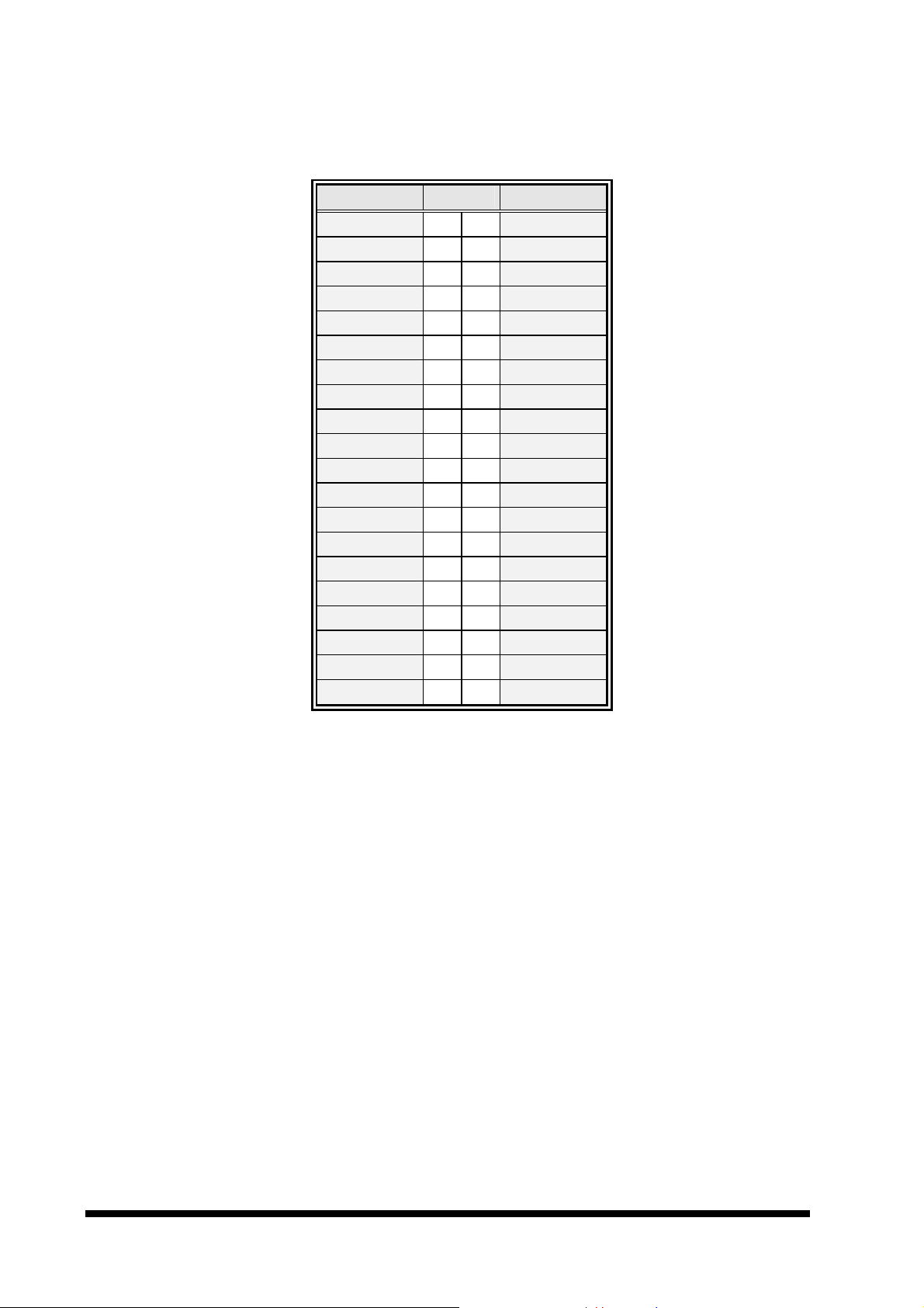
User’s Manual
3.7.17 IDE Connector (CN5)
Signal PIN Signal
GND 40 39
DCS3# 38 37
DA2 36 35
NC 34 33
NC 32 31
GND 30 29
GND 28 27
GND 26 25
GND 24 23
GND 22 21
NC 20 19
D15 18 17
D14 16 15
D13 14 13
D12 12 11
D11 10 9 D4
D10 8 7 D5
D9 6 5 D6
D8 4 3 D7
GND 2 1 RESET#
DACT#
DCS1#
DA0
DA1
IRQ14
DACK#
IORDY
IOR#
IOW#
DREQ
GND
D0
D1
D2
D3
34 ECM-3610/3610L User’s Manual
Page 47
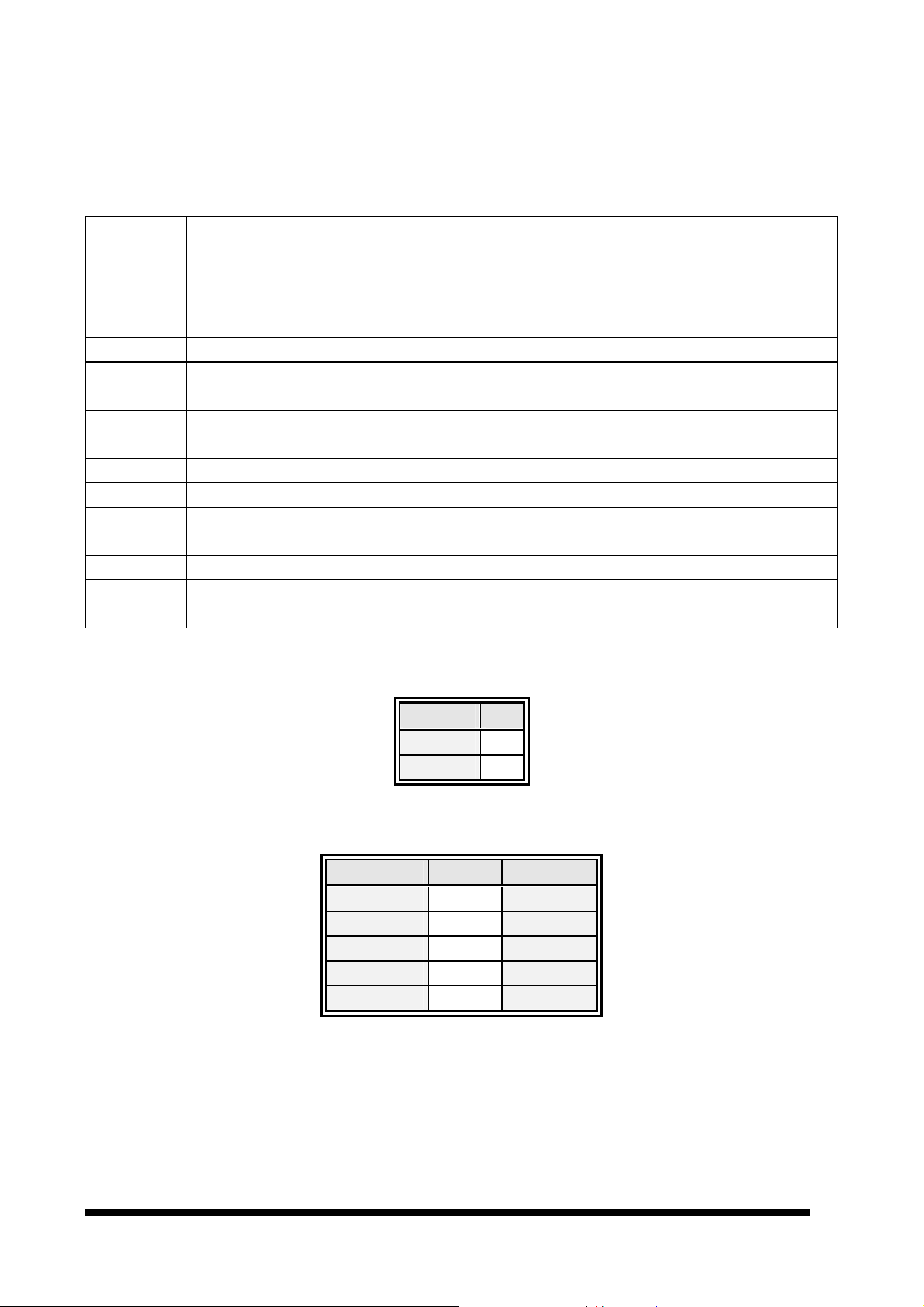
ECM-3610/3610L
direction of the
3.7.18 Signal Description – IDE Connector (CN5)
The IDE interface supports PIO modes 0 to 4 and Bus Master IDE. Data transfer rates up
to 100 MB/Sec is possible.
DA [2:0] IDE Address Bits. These address bits are used to access a register or data port in a device
on the IDE bus.
DCS1#,
DCS3#
D [15:0] IDE Data Lines. D [15:0] transfers data to/from the IDE devices.
IOR# IDE I/O Read. Signal is asserted on read accesses to the corresponding IDE port addresses.
IOW# IDE I/O Write. Each signal is asserted on write accesses to corresponding the IDE port
IORDY When deasserted, these signals extend the transfer cycle of any host register access when
RESET# IDE Reset . This signal resets all the devices that are attached to the IDE interface.
IRQ14 Interrupt line from hard disk. Connected directly to PC-AT bus.
DREQ The DREQ is used to request a DMA transfer from the South Bridge. The
DACK# DMA Acknowledge. The DACK# acknowledges the DREQ request to initiate DMA transfers.
DACT# Signal from hard disk indicating hard disk activity. The signal level depends on the hard disk
IDE Chip Selects. The chip select signals are used to select the command block registers in
an IDE device. DCS1# selects the primary hard disk.
addresses.
the device is not ready to respond to the data transfer request.
transfers is determined by the IOR#/IOW# signals.
type, normally active low. The signal is routed directly to the LED1.
3.7.19 System Fan Connector (CN6)
3.7.20 Audio Connector (CN7)
Signal PIN Signal
NC 10 9
Mic Bias 8 7
Line-In L 6 5 Line-In R
GND 4 3
Line-Out L 2 1 Line-Out R
Signal PIN
VCC 2
GND 1
NC
Mic-In
GND
ECM-3610/3610L User’s Manual 35
Page 48
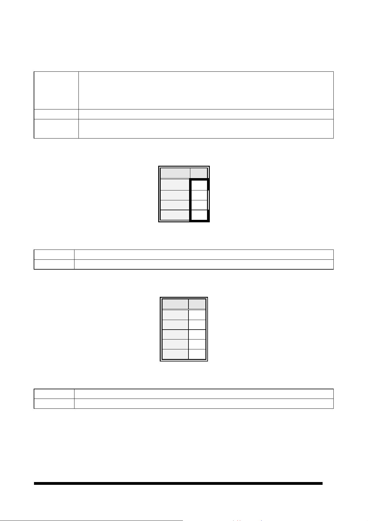
User’s Manual
3.7.21 Signal Description – Audio Connector (CN7)
Mic-In / Mic
Bias
Line-In L/R Left and right line in signals.
Line-Out L/R Left and right line out signals. Both signals are capacitor coupled and should have GND as
The MIC signal is used for microphone input. This input is fed to the left microphone
channel.
Mic Bias provides 3.3V supplied through 3.2K Ω with capacitive decoupling to GND. This
signal may be used for bias of some microphone types.
return.
3.7.22 CD-ROM Audio Input Connector (CN8)
Signal PIN
CD_GND 1
CD_L 2
CD_GND 3
CD_R 4
3.7.23 Signal Description – CD-ROM Audio Input Connector (CN8)
CD_L/R Left and right CD audio input lines.
CD_GND GND for left and right CD. This GND level is not connected to the board GND.
3.7.24 IrDA Connector (CN9)
Signal PIN
VCC 1
NC 2
IRRX 3
GND 4
IRTX 5
3.7.25 Signal Description – IrDA Connector (CN9)
IRRX Infrared Receiver input
IRTX Infrared Transmitter output
36 ECM-3610/3610L User’s Manual
Page 49
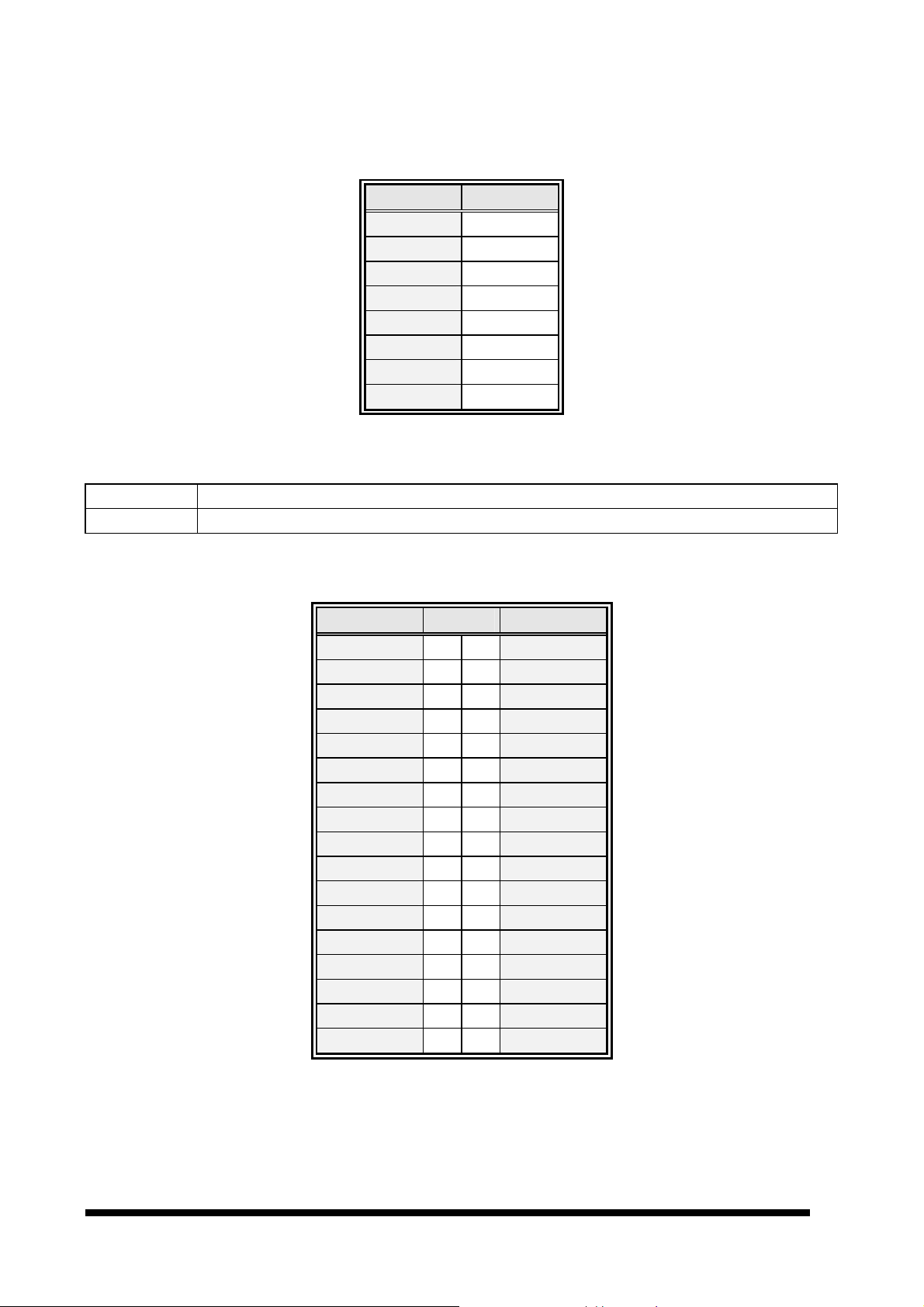
ECM-3610/3610L
3.7.26 10/100BASE-Tx Ethernet Connector (CN10, CN11)
Signal PIN
TXD+ 1
TXD- 2
RXD+ 3
NC 4
NC 5
RXD- 6
NC 7
NC 8
3.7.27 Signal Description – 10/100Base-Tx Ethernet Connector (CN10, CN11)
TXD+ / TXD- Ethernet 10/100Base-Tx differential transmitter outputs.
RXD+ / RXD- Ethernet 10/100Base-Tx differential receiver inputs.
3.7.28 Floppy Connector (FLP1)
Signal PIN Signal
GND 1 2 DRVDEN0#
GND 3 4 NC
GND 5 6 DRVDEN1#
GND 7 8 INDEX#
GND 9 10
GND 11 12
GND 13 14
GND 15 16
GND 17 18
GND 19 20
GND 21 22
GND 23 24
GND 25 26
GND 27 28
GND 29 30
GND 31 32
GND 33 34 DSKCHG#
MOA#
DSB#
DSA#
MOB#
DIR#
STEP#
WD#
WE#
TRAK0#
WPT#
RDATA#
SIDE1#
ECM-3610/3610L User’s Manual 37
Page 50

User’s Manual
the diskette is
3.7.29 Signal Description – Floppy Connector (FLP1)
RDATA# The read data input signal from the FDD.
WD# Write data. This logic low open drain writes pre-compensation serial data to the selected
FDD. An open drain output.
WE# Write enable. An open drain output.
MOA# Motor A On. When set to 0, this pin enables disk drive 0. This is an open drain output.
MOB# Motor B On. When set to 0, this pin enables disk drive 1. This is an open drain output.
DSA# Drive Select A. When set to 0, this pin enables disk drive A. This is an open drain output .
DSB# Drive Select B. When set to 0, this pin enables disk drive B. This is an open drain output .
SIDE1# This output signal selects side of the disk in the selected drive.
DIR# Direction of the head step motor. An open drain output
Logic 1 = outward motion
Logic 0 = inward motion
STEP# Step output pulses. This active low open drain output produces a pulse to move the head to
another track.
DRVDEN0/1# This output indicates whether a low drive density (250/300kbps at low level) or a high drive
density (500/1000kbps at high level) has been selected.
TRAK0# Track 0. This Schmitt-triggered input from the disk drive is active low when the head is
positioned over the outermost track.
INDEX# This Schmitt-triggered input from the disk drive is active low when the head is positioned
over the beginning of a track marked by an index hole.
WP# Write protected. This active low Schmitt input from the disk drive indicates that
write-protected.
DSKCHG# Diskette change. This signal is active low at power on and whenever the diskette is removed.
38 ECM-3610/3610L User’s Manual
Page 51
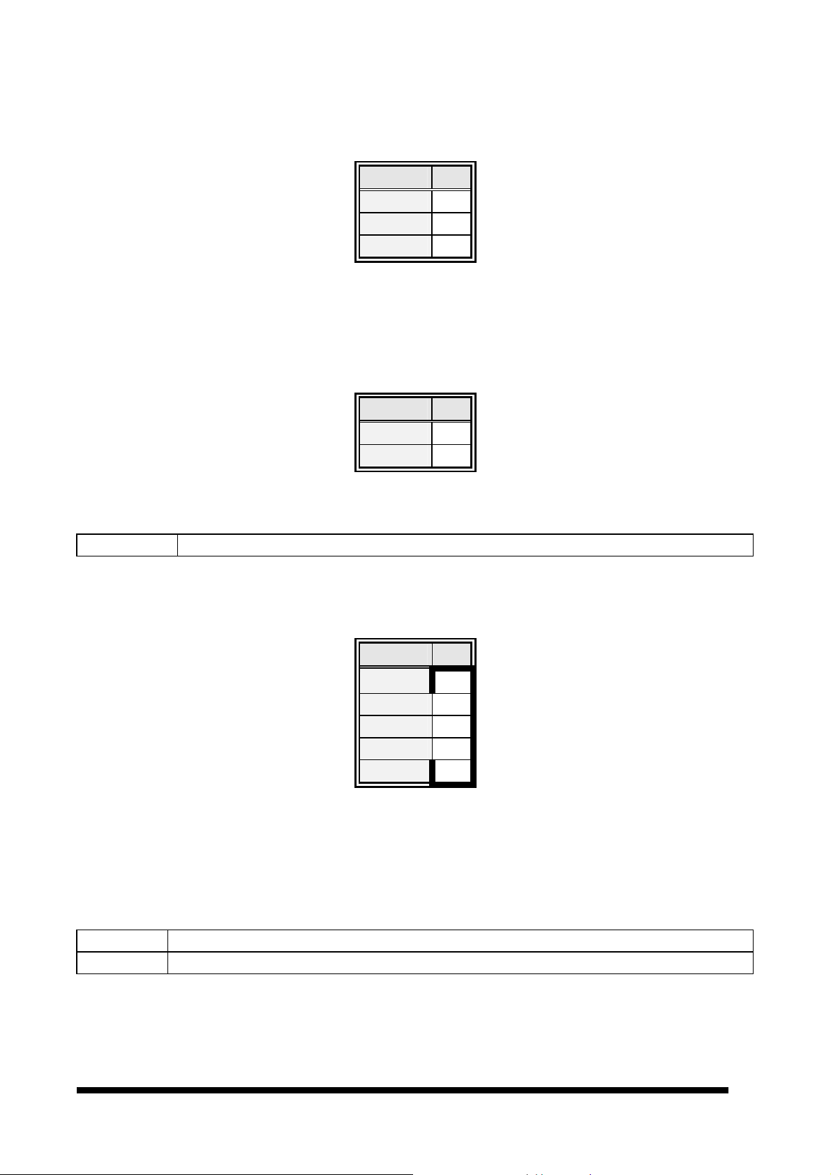
3.7.30 ATX Power Connector (J1)
Note:
Set J1 to 2-3 closed. If AT power supply is to be used.
3.7.31 ATX Soft-power Bottom (J2)
ECM-3610/3610L
Signal PIN
PS_ON# 1
VCC 2
VCC_SB 3
Signal PIN
PWRBTN 1
GND 2
3.7.32 Signal Description – ATX Soft-power Bottom (J2)
PWBTN Power Button
3.7.33 LCD Inverter Connector (J3)
Signal PIN
VCC 5
VR 4
ENBKL 3
GND 2
+12V 1
Note:
For inverters with adjustable Backlight function, it is possible to control the
LCD brightness through the VR signal (pin 4) controlled by VR1. Please see
the VR1 section for detailed circuitry information.
3.7.34 Signal Description – LCD Inverter Connector (J3)
VR Vadj = 5V ~ 0V.
ENBKL LCD backlight ON/OFF control signal.
ECM-3610/3610L User’s Manual 39
Page 52
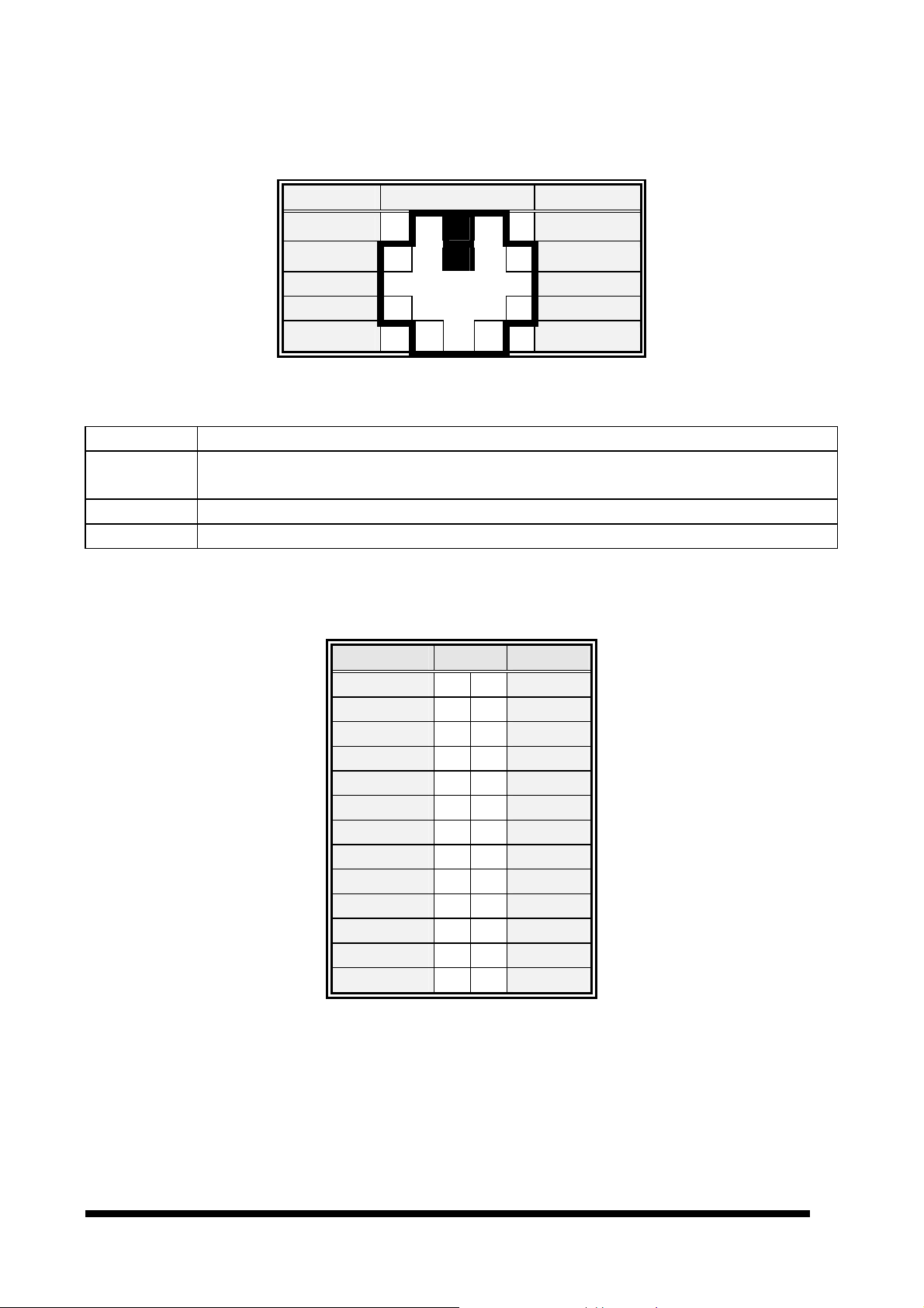
User’s Manual
2
3.7.35 Keyboard and PS/2 Mouse Connector (KB1)
Signal PIN Signal
MCLK 6 5
VCC 4 3
MDAT
1
KCLK
GND
KDAT
3.7.36 Signal Description – Keyboard & PS/2 Mouse Connectors (KB1)
KCLK Bi-directional clock signal used to strobe data/commands from/to the PC-AT keyboard.
KDAT Bi-directional serial data line used to transfer data from or commands to the PC-AT
keyboard.
MCLK Bi-directional clock signal used to strobe data/commands from/to the PS/2 mouse.
MDAT Bi-directional serial data line used to transfer data from or commands to the PS/2 mouse.
3.7.37 Parallel Port Connector (PNT1)
Signal PIN Signal
STB# 1 2
PD0 3 4
PD1 5 6
PD2 7 8
PD3 9 10
PD4 11 12
PD5 13 14
PD6 15 16
PD7 17 18
ACK# 19 20
BUSY 21 22
PE 23 24
SLCT 25 26
AFD#
ERR#
INIT#
SLIN#
GND
GND
GND
GND
GND
GND
GND
GND
GND
40 ECM-3610/3610L User’s Manual
Page 53
3.7.38 DB25 Parallel Port Connector (PNT1)
Signal PIN Signal
STB# 1
ECM-3610/3610L
14
PD0 2
15
PD1 3
16
PD2 4
17
PD3 5
18
PD4 6
19
PD5 7
20
PD6 8
21
PD7 9
22
ACK# 10
23
BUSY 11
24
PE 12
25
AFD#
ERR#
INIT#
SLIN#
GND
GND
GND
GND
GND
GND
GND
GND
SLCT 13
ECM-3610/3610L User’s Manual 41
Page 54
User’s Manual
3.7.39 Signal Description – Parallel Port Connector (PNT1)
The following signal description covers the signal definitions, when the parallel port is
operated in standard centronic mode. The parallel port controller also supports the fast
EPP and ECP modes.
PD [7:0] Parallel data bus from PC board to printer. The data lines are able to operate in PS/2
compatible bi-directional mode.
SLIN# Output line for detection of printer selection. This pin is pulled high internally.
SLCT An active high input on this pin indicates that the printer is selected. This pin is pulled high
internally.
STB# An active low output is used to latch the parallel data into the printer. This pin is pulled high
internally.
BUSY An active high input indicates that the printer is not ready to receive data. This pin is pulled
high internally.
ACK# An active low input on this pin indicates that the printer has received data and is ready to
accept more data. This pin is pulled high internally.
INIT# Output line for the printer initialization. This pin is pulled high internally.
AFD# An active low output from this pin causes the printer to auto feed a line after a line is printed.
This pin is pulled high internally.
ERR# An active low input on this pin indicates that the printer has encountered an error condition.
This pin is pulled high internally.
PE An active high input on this pin indicates that the printer has detected the end of the paper.
This pin is pulled high internally.
3.7.40 Auxiliary Power Connector (PWR1)
Signal PIN
-12v 4
GND 3
GND 2
-5V 1
3.7.41 Power Connector (PWR2)
Signal PIN
5V 4
GND 3
GND 2
12V 1
42 ECM-3610/3610L User’s Manual
Page 55
3.7.42 USB Connector (USB1)
ECM-3610/3610L
Signal
VCC1 1 2 GND
D1- 3 4 GND
D1+ 5 6 D2+
GND 7 8 D2GND 9 10
PIN
CH1 CH2
Signal
VCC2
3.7.43 Signal Description – USB Connector (USB1)
D1+ / D1- Differential bi-directional data signal for USB channel 0. Clock is transmitted along with the
data using NRZI encoding. The signalling bit rate is up to 12 Mbs.
D2+ / D2- Differential bi-directional data signal for USB channel 1. Clock is transmitted along with the
data using NRZI encoding. The signalling bit rate is up to 12 Mbs.
VCC 5 V DC supply for external devices. Maximum load according to USB standard.
ECM-3610/3610L User’s Manual 43
Page 56
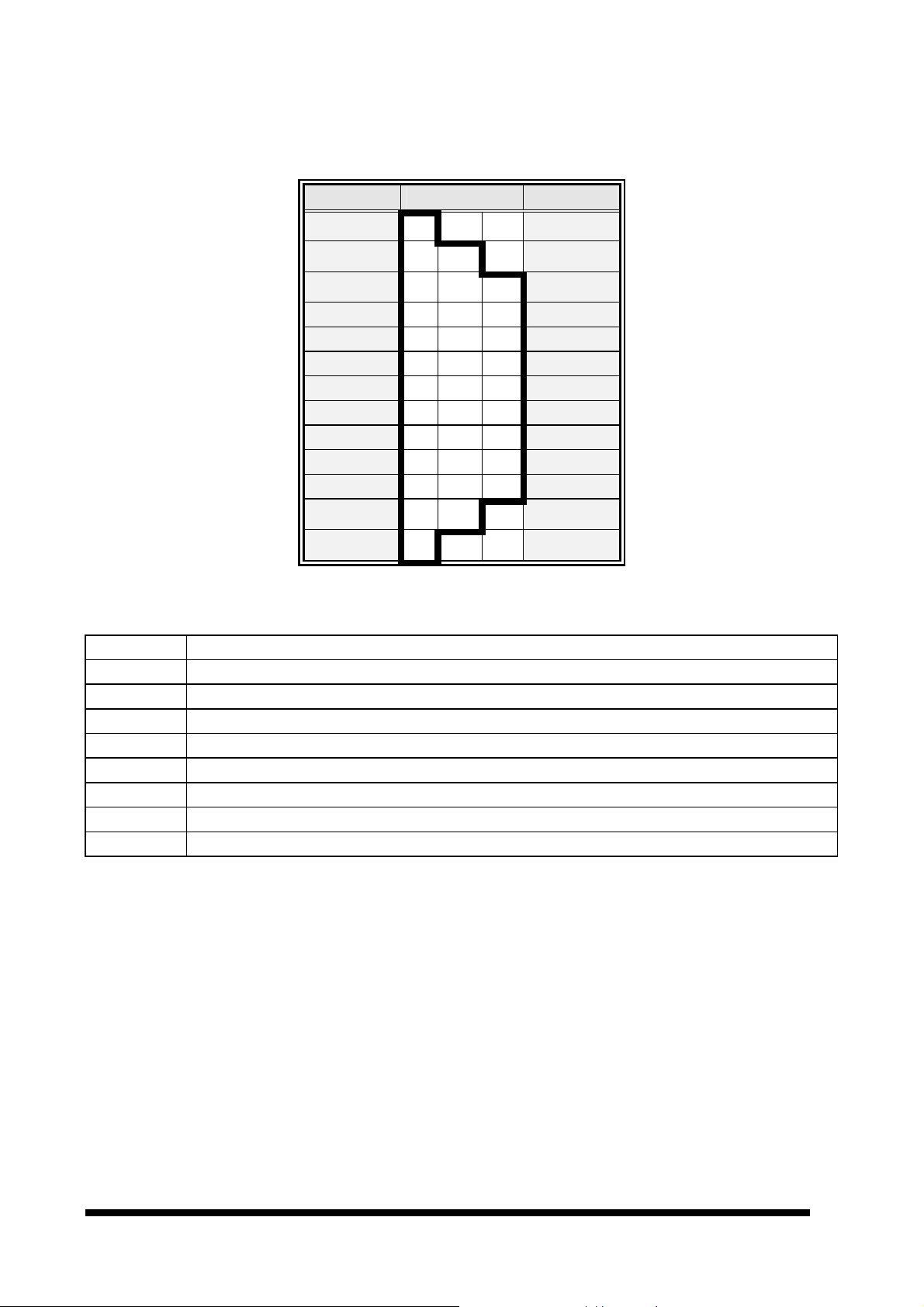
User’s Manual
3.7.44 CRT Connector (VGA1)
Signal PIN Signal
6 ANA-GND
RED 1 11
7 ANA-GND
GREEN 2 12 DDCDAT
8 ANA-GND
BLUE 3 13
9 VCC
NC 4 14
10
DIG-GND 5 15 DDCCLK
DIG-GND
NC
HSYNC
VSYNC
3.7.45 Signal Description – CRT Connector (VGA1)
HSYNC CRT horizontal synchronisation output .
VSYNC CRT vertical synchronisation output.
DDCCLK Display Data Channel Clock. Used as clock signal to/from monitors with DDC interface.
DDCDAT Display Data Channel Data. Used as data signal to/from monitors with DDC interface.
RED
GREEN
BLUE
DIG-GND Ground reference for HSYNC and VSYNC.
ANA-GND Ground reference for RED, GREEN, and BLUE.
Analog output carrying the red colour signal to the CRT. For 75 O cable impedance.
Analog output carrying the green colour signal to the CRT. For 75 O cable impedance.
Analog output carrying the blue colour signal to the CRT. For 75 O cable impedance.
44 ECM-3610/3610L User’s Manual
Page 57
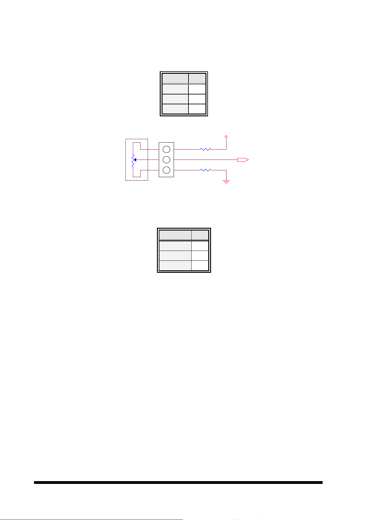
1 2 3
3.7.46 LCD Backlight Brightness Adjustment Connector (VR1)
Signal PIN
GND 1
VR 2
VCC 3
VR1
ECM-3610/3610L
VCC
J3 pin 4
Variation Resistor (Recommended: 4.7K? , >1/16W)
3.7.47 STN LCD Contrast Adjustment Connector (VR2)
Signal PIN
GND 1
VCON 2
VCC 3
ECM-3610/3610L User’s Manual 45
Page 58

User’s Manual
4. AWARD BIOS Setup
4.1 Starting Setup
The AwardBIOS™ is immediately activated when you first power on the computer. The
BIOS reads the system information contained in the CMOS and begins the process of
checking out the system and configuring it. When it finishes, the BIOS will seek an
operating system on one of the disks and then launch and turn control over to the
operating system.
While the BIOS is in control, the Setup program can be activated in one of two ways:
By pressing <Del> immediately after switching the system on, or
By pressing the <Del> key when the following message appears briefly at the bottom of
the screen during the POST (Power On Self Test).
Press DEL to enter SETUP
If the message disappears before you respond and you still wish to enter Setup, restart
the system to try again by turning it OFF then ON or pressing the "RESET" button on the
system case. You may also restart by simultaneously pressing <Ctrl>, <Alt>, and
<Delete> keys. If you do not press the keys at the correct time and the system does not
boot, an error message will be displayed and you will again be asked to.
Press F1 To Continue, DEL to enter SETUP
46 ECM-3610/3610L User’s Manual
Page 59

ECM-3610/3610L
4.2 Using Setup
In general, you use the arrow keys to highlight items, press <Enter> to select, use the
PageUp and PageDown keys to change entries, press <F1> for help and press <Esc> to
quit. The following table provides more detail about how to navigate in the Setup program
using the keyboard.
Up arrow Move to previous item
Down arrow Move to next item
Left arrow Move to the item in the left hand
Right arrow Move to the item in the right hand
Esc key Main Menu -- Quit and not save changes into CMOS
Status Page Setup Menu and Option Page Setup Menu -- Exit
current page and return to Main Menu
PgUp key Increase the numeric value or make changes
PgDn key Decrease the numeric value or make changes
+ key Increase the numeric value or make changes
- key Decrease the numeric value or make changes
F1 key General help, only for Status Page Setup Menu and Option Page
Setup Menu
(Shift) F2 key Change color from total 16 colors. F2 to select color forward,
(Shift) F2 to select color backward
F3 key Calendar, only for Status Page Setup Menu
F4 key Reserved
F5 key Restore the previous CMOS value from CMOS, only for Option
Page Setup Menu
F6 key Load the default CMOS value from BIOS default table, only for
Option Page Setup Menu
F7 key Load the default
F8 key Reserved
F9 key Reserved
F10 key Save all the CMOS changes, only for Main Menu
Table 1 : Legend Keys
4.2.1 Navigating Through The Menu Bar
Use the left and right arrow keys to choose the menu you want to be in.
4.2.2 To Display a Sub Menu
Use the arrow keys to move the cursor to the sub menu you want. Then press <Enter>. A
“Ø” pointer marks all sub menus.
ECM-3610/3610L User’s Manual 47
Page 60
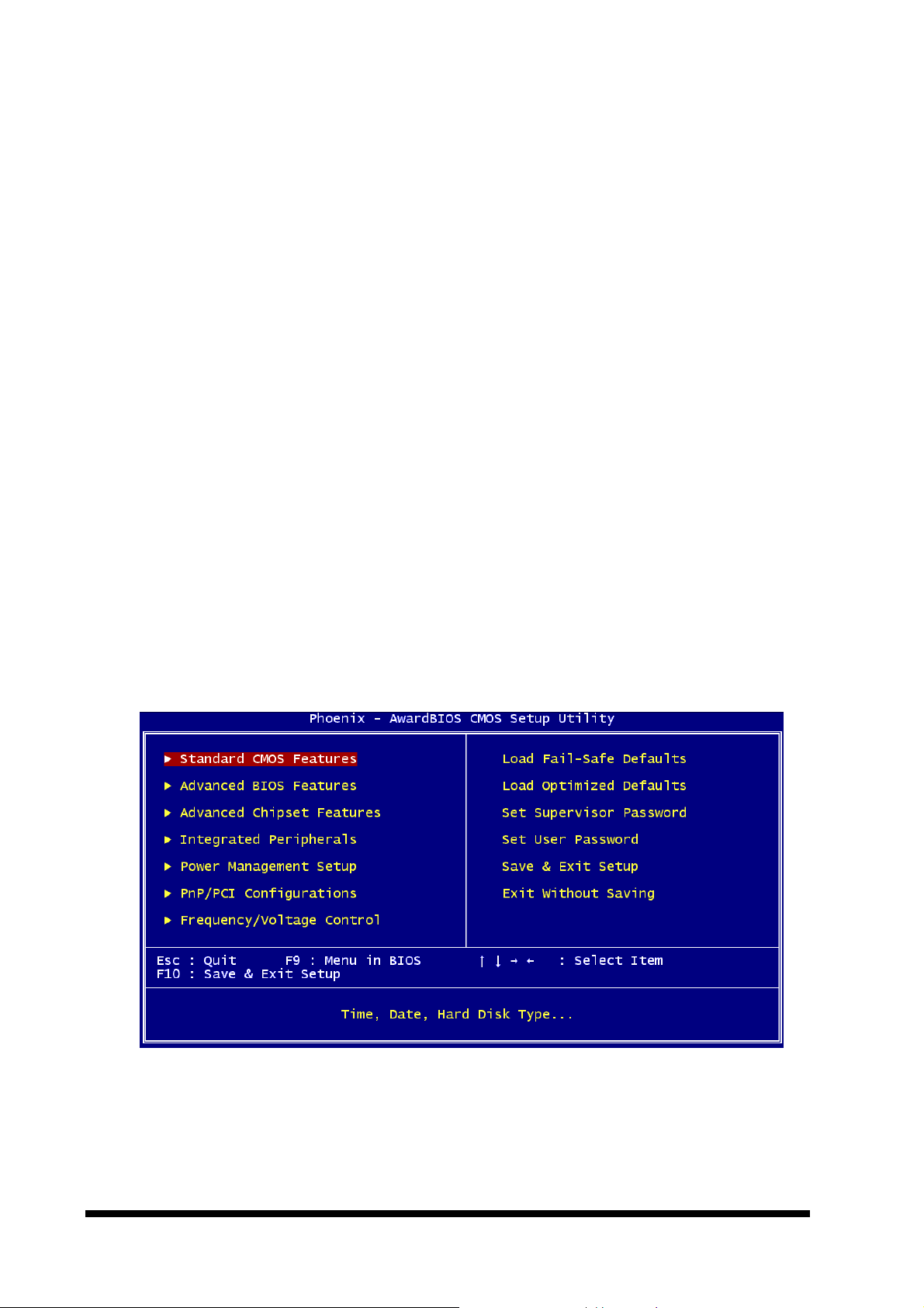
User’s Manual
4.3 Getting Help
Press F1 to pop up a small help window that describes the appropriate keys to use and
the possible selections for the highlighted item. To exit the Help Window press <Esc> or
the F1 key again.
4.4 In Case of Problems
If, after making and saving system changes with Setup, you discover that your computer
no longer is able to boot, the AwardBIOS™ supports an override to the CMOS settings
which resets your system to its defaults.
The best advice is to only alter settings which you thoroughly understand. To this end, we
strongly recommend that you avoid making any changes to the chipset defaults. These
defaults have been carefully chosen by both Award and your systems manufacturer to
provide the absolute maximum performance and reliability. Even a seemingly small
change to the chipset setup has the potential for causing you to use the override.
4.5 Main Menu
Once you enter the AwardBIOS™ CMOS Setup Utility, the Main Menu will appear on the
screen. The Main Menu allows you to select from several setup functions and two exit
choices. Use the arrow keys to select among the items and press <Enter> to accept and
enter the sub-menu.
Note that a brief description of each highlighted selection appears at the bottom of the
screen.
48 ECM-3610/3610L User’s Manual
Page 61

ECM-3610/3610L
4.5.1 Setup Items
The main menu includes the following main setup categories. Recall that some systems
may not include all entries.
4.5.1.1 Standard CMOS Features
Use this menu for basic system configuration.
4.5.1.2 Advanced BIOS Features
Use this menu to set the Advanced Features available on your system.
4.5.1.3 Advanced Chipset Features
Use this menu to change the values in the chipset registers and optimize your system's
performance.
4.5.1.4 Integrated Peripherals
Use this menu to specify your settings for integrated peripherals.
4.5.1.5 Power Management Setup
Use this menu to specify your settings for power management.
4.5.1.6 PNP / PCI Configuration
This entry appears if your system supports PnP / PCI.
4.5.1.7 Frequency / Voltage Control
Use this menu to specify your settings for frequency/voltage control.
4.5.1.8 Load Fail-Safe Defaults
Use this menu to load the BIOS default values for the minimal/stable performance for your
system to operate.
4.5.1.9 Load Optimized Defaults
Use this menu to load the BIOS default values that are factory settings for optimal
performance system operations. While Award has designed the custom BIOS to maximize
performance, the factory has the right to change these defaults to meet their needs.
ECM-3610/3610L User’s Manual 49
Page 62

User’s Manual
4.5.1.10 Supervisor / User Password
Use this menu to set User and Supervisor Passwords.
4.5.1.11 Save & Exit Setup
Save CMOS value changes to CMOS and exit setup.
4.5.1.12 Exit Without Save
Abandon all CMOS value changes and exit setup.
50 ECM-3610/3610L User’s Manual
Page 63
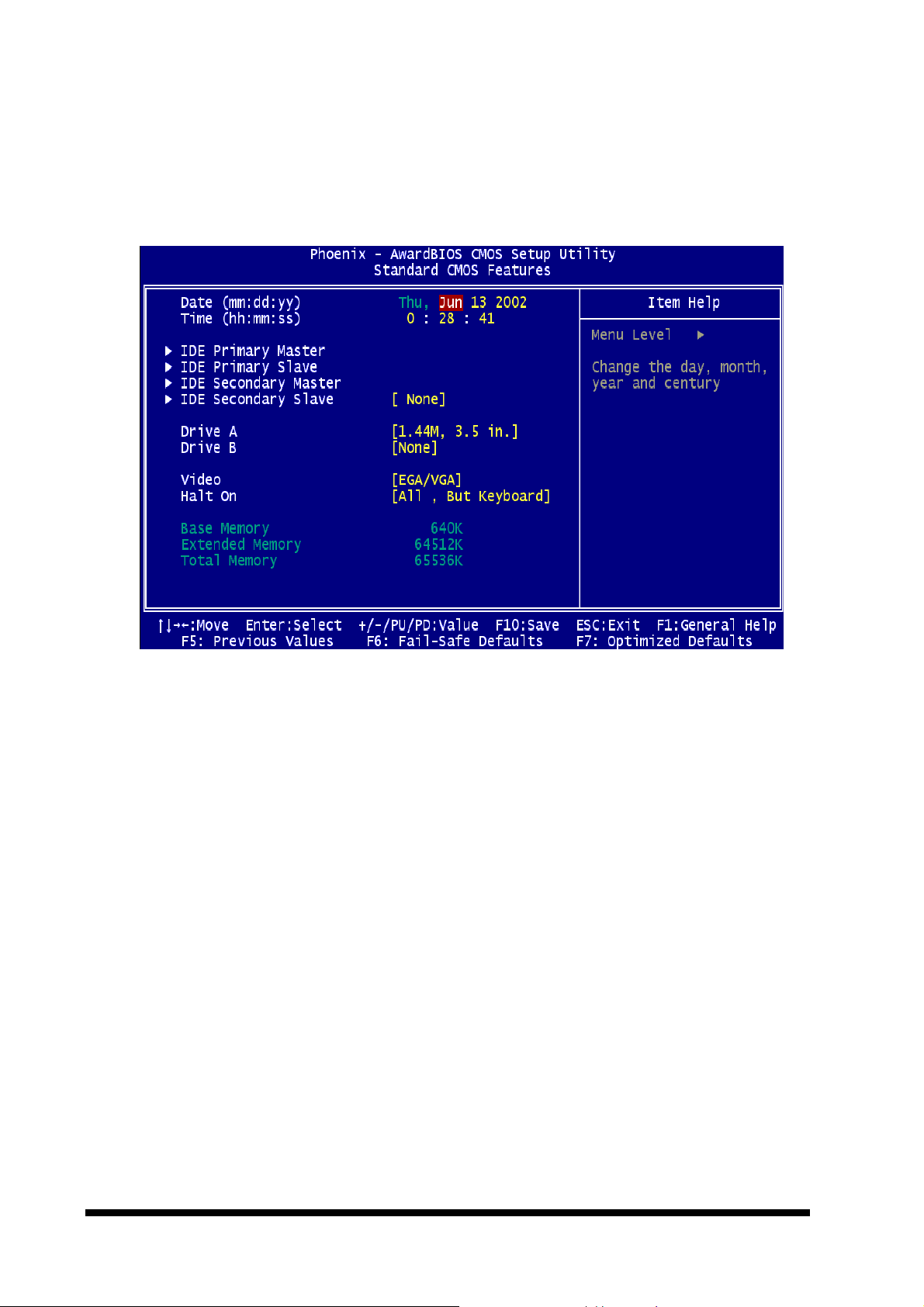
ECM-3610/3610L
4.5.2 Standard CMOS Setup
The items in Standard CMOS Setup Menu are divided into 10 categories. Each category
includes no, one or more than one setup items. Use the arrow keys to highlight the item
and then use the <PgUp> or <PgDn> keys to select the value you want in each item.
Figure 1 : The Main Menu
ECM-3610/3610L User’s Manual 51
Page 64

User’s Manual
4.5.2.1 Main Manu Selection
This table shows the selections that you can make on the Main Menu.
Item Options Description
Date Month DD YYYY Set the system date. Note that the
‘Day’ automatically changes when
you set the date
Time HH : MM : SS Set the system time
IDE Primary Master Options are in its sub menu
(described in Table 3)
IDE Primary Slave Options are in its sub menu
(described in Table 3)
IDE Secondary Master Options are in its sub menu
(described in Table 3)
IDE Secondary Master Options are in its sub menu
(described in Table 3)
Drive A
Drive B
Video EGA/VGA
Halt On All Errors
Base Memory N/A Displays the amount of conventional
Extended Memory N/A Displays the amount of extended
Total Memory N/A Displays the total memory available
None
360K, 5.25 in
1.2M, 5.25 in
720K, 3.5 in
1.44M, 3.5 in
2.88M, 3.5 in
CGA 40
CGA 80
MONO
No Errors
All, but Keyboard
All, but Diskette
All, but Disk/Key
Press <Enter> to enter the sub menu
of detailed options
Press <Enter> to enter the sub menu
of detailed options
Press <Enter> to enter the sub menu
of detailed options
Press <Enter> to enter the sub menu
of detailed options
Select the type of floppy disk drive
installed in your system
Select the default video device
Select the situation in which you
want the BIOS to stop the POST
process and notify you
memory detected during boot up
memory detected during boot up
in the system
Table 2 : Main Menu Selections
52 ECM-3610/3610L User’s Manual
Page 65

ECM-3610/3610L
4.5.2.2 IDE Adapters
The IDE adapters control the hard disk drive. Use a separate sub menu to configure each
hard disk drive.
Figure 2 shows the IDE primary master sub menu.
Use the legend keys to navigate through this menu and exit to the main menu. Use Table
3 to configure the hard disk.
Item Options Description
Press Enter to auto-detect the HDD
IDE HDD Auto-detection
IDE Primary Master
Capacity
Access Mode
The following options are selectable only if the ‘IDE Primary Master’ item is set to ‘Manual’
Cylinder
Head
Precomp
Landing zone
Sector
Auto Display your disk drive
Press Enter
None
Auto
Manual
size
Normal
LBA
Large
Auto
Min = 0
Max = 65535
Min = 0
Max = 255
Min = 0
Max = 65535
Min = 0
Max = 65535
Min = 0
Max = 255
on this channel. If detection is
successful, it fills the remaining fields
on this menu.
Selecting ‘manual’ lets you set the
remaining fields on this screen.
Selects the type of fixed disk. "User
Type" will let you select the number
of cylinders, heads, etc. Note:
PRECOMP=65535 means NONE !
Disk drive capacity (Approximated).
Note that this size is usually slightly
greater than the size of a formatted
disk given by a disk checking
program.
Choose the access mode for this
hard disk
Set the number of cylinders for this
hard disk.
Set the number of read/write heads
**** Warning: Setting a value of
65535 means no hard disk
****
Number of sectors per track
Table 3 : Hard disk selections
ECM-3610/3610L User’s Manual 53
Page 66
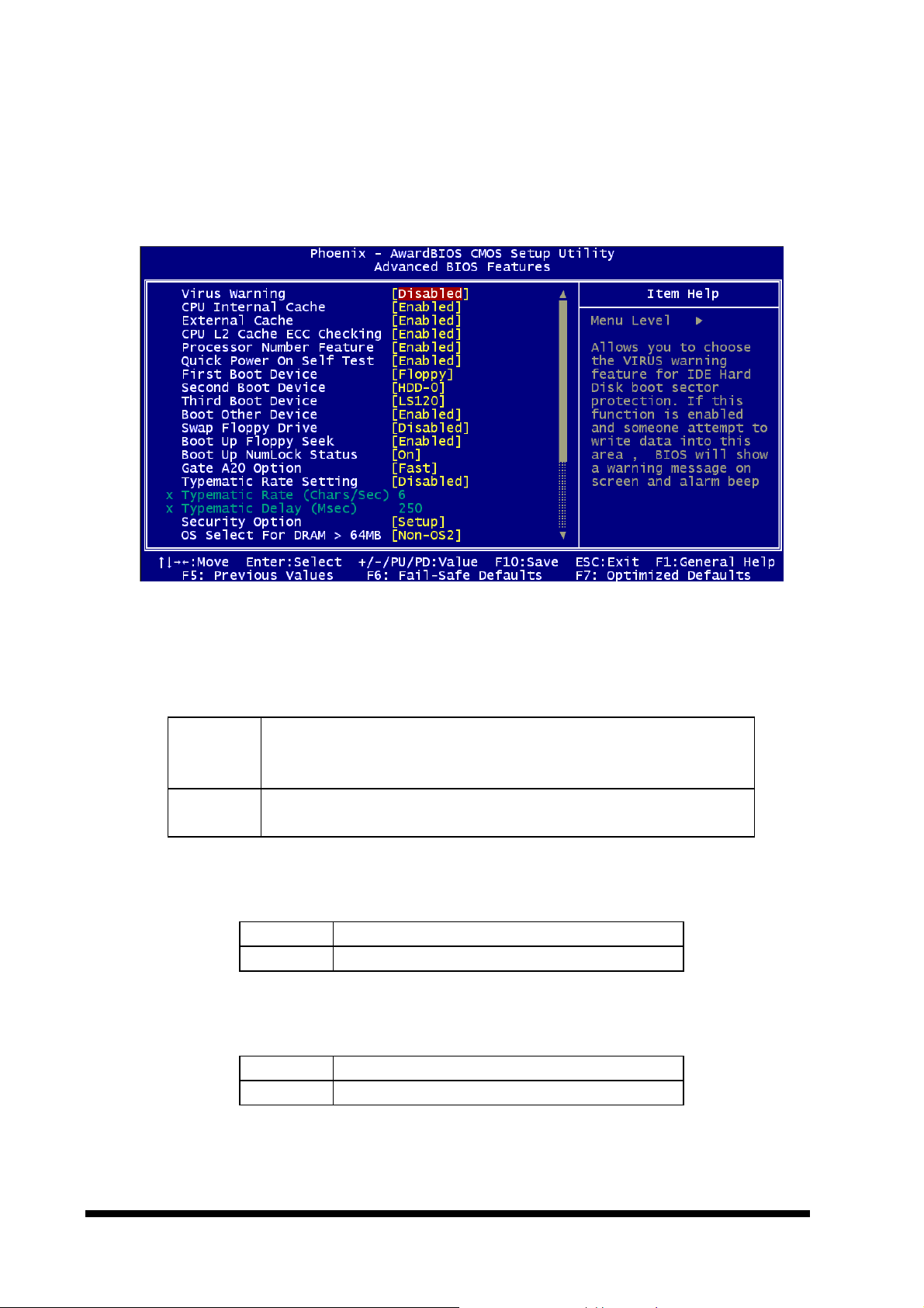
User’s Manual
4.5.3 Advanced BIOS Features
This section allows you to configure your system for basic operation. You have the
opportunity to select the system’s default speed, boot-up sequence, keyboard operation,
shadowing and security.
4.5.3.1 Virus Warning
Allows you to choose the VIRUS Warning feature for IDE Hard Disk boot sector protection.
If this function is enabled and someone attempt to write data into this area, BIOS will show
a warning message on screen and alarm beep.
Enabled Activates automatically when the system boots up causing a warning
message to appear when anything attempts to access the boot sector
or hard disk partition table.
Disabled No warning message will appear when anything attempts to access
the boot sector or hard disk partition table.
4.5.3.2 CPU Internal Cache
This item allows you to speed up memory access. However, it depends on CPU design.
Enabled Enable cache
Disabled Disable cache
4.5.3.3 External Cache
This item allows you to speed up memory access. However, it depends on chipset design.
Enabled Enable cache
Disabled Disable cache
54 ECM-3610/3610L User’s Manual
Page 67
ECM-3610/3610L
4.5.3.4 CPU L2 Cache ECC Checking
This item allows you to enable/disable CPU L2 Cache ECC checking.
Enabled Enable L2 Cache ECC Checking
Disabled Disable L2 Cache ECC Checking
4.5.3.5 Quick Power On Self Test
This category speeds up Power On Self Test (POST) after you power up the computer. If
it is set to Enable, BIOS will shorten or skip some check items during POST.
Enabled Enable quick POST
Disabled Normal POST
4.5.3.6 First/Second/Third/Other Boot Device
The BIOS attempts to load the operating system from the devices in the sequence
selected in these items.
Floppy Floppy Device
LS120 LS120 Device
HDD-0 First Hard Disk Device
SCSI SCSI Device
CDROM CDROM Device
HDD-1 Secondary Hard Disk Device
HDD-2 Third Hard Disk Device
HDD-3 Fourth Hard Disk Device
ZIP100 ZIP-100 Device
USB-FDD USB Floppy Device
USB-ZIP USB ZIP Device
USB-CDROM USB CDROM Device
USB-HDD USB Hard Disk Device
LAN Network Device
Disabled Disabled any boot device
4.5.3.7 Boot Up Floppy Seek
Seeks disk drives during boot up. Disabling speeds boot up.
4.5.3.8 Boot Up NumLock Status
Select power on state for NumLock.
Enabled Enable Floppy Seek
Disabled Disable Floppy Seek
Enabled Enable NumLock
Disabled Disable NumLock
ECM-3610/3610L User’s Manual 55
Page 68

User’s Manual
4.5.3.9 Gate A20 Option
Select if chipset or keyboard controller should control GateA20.
Normal A pin in the keyboard controller controls
GateA20
Fast Lets chipset control GateA20
4.5.3.10 Typematic Rate Setting
Key strokes repeat at a rate determined by the keyboard controller. When enabled, the
typematic rate and typematic delay can be selected.
The choice: Enabled/Disabled.
4.5.3.11 Typematic Rate (Chars/Sec)
Sets the number of times a second to repeat a key stroke when you hold the key down.
The choice: 6, 8, 10, 12, 15, 20, 24, or 30.
4.5.3.12 Typematic Delay (Msec)
Sets the delay time after the key is held down before it begins to repeat the keystroke.
The choice: 250, 500, 750, or 1000.
4.5.3.13 Security Option
Select whether the password is required every time the system boots or only when you
enter setup.
System The system will not boot and access to Setup will be denied if the
correct password is not entered at the prompt.
Setup The system will boot, but access to Setup will be denied if the correct
password is not entered at the prompt.
Note: To disable security, select PASSWORD SETTING at Main Menu and then you will
be asked to enter password. Do not type anything and just press <Enter>, it will
disable security. Once the security is disabled, the system will boot and you can
enter Setup freely.
4.5.3.14 OS Select for DRAM > 64MB
Select the operating system that is running with greater than 64MB of RAM on the system.
The choice: Non-OS2, OS2.
56 ECM-3610/3610L User’s Manual
Page 69
ECM-3610/3610L
4.5.3.15 Video BIOS Shadow
Determines whether video BIOS will be copied to RAM. However, it is optional depending
on chipset design. Video Shadow will increase the video speed.
Enabled Video shadow is enabled
Disabled Video shadow is disabled
4.5.3.16 C8000 – CBFFF Shadow/DC000 – DFFFF Shadow
These categories determine whether option ROMs will be copied to RAM. An example of
such option ROM would be support of on-board SCSI.
Enabled Optional shadow is enabled
Disabled Optional shadow is disabled
4.5.3.17 Small Logo (EPA) Show
This item allows you enabled/disabled the small EPA logo show on screen at the POST
step,
Enabled EPA Logo show is enabled
Disabled EPA Logo show is disabled
ECM-3610/3610L User’s Manual 57
Page 70
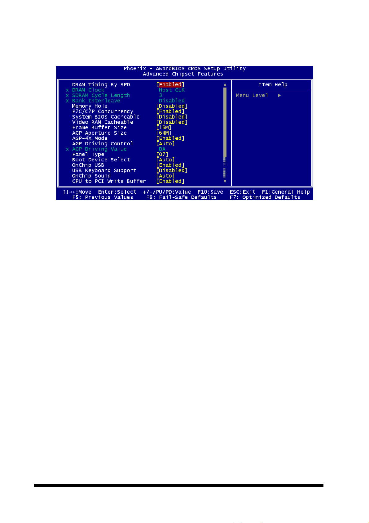
User’s Manual
4.5.4 Advanced Chipset Features
This section allows you to configure the system based on the specific features of the
installed chipset. This chipset manages bus speeds and access to system memory
resources, such as DRAM and the external cache. It also coordinates communications
between the conventional ISA bus and the PCI bus. It must be stated that these items
should never need to be altered. The default settings have been chosen because they
provide the best operating conditions for your system. The only time you might consider
making any changes would be if you discovered that data was being lost while using your
system.
The first chipset settings deal with CPU access to dynamic random access memory
(DRAM). The default timings have been carefully chosen and should only be altered if
data is being lost. Such a scenario might well occur if your system had mixed speed
DRAM chips installed so that greater delays may be required to preserve the integrity of
the data held in the slower memory chips.
4.5.4.1 DRAM Timing by SPD
This item allows you to select the SDRAM timing value by SPD data.
The Choice: Enabled, Disabled.
4.5.4.2 DRAM Clock
This item allows you to set DRAM clock speed.
The Choice: Host CLK, HCLK-33M, HCLK+33M.
58 ECM-3610/3610L User’s Manual
Page 71

ECM-3610/3610L
4.5.4.3 SDRAM Cycle Length
When synchronous DRAM is installed, the number of clock cycles of CAS latency
depends on the DRAM timing. Do not reset this field from the default value specified by
the system designer.
The Choice: 2, 3.
4.5.4.4 Bank Interleave
Set SDRAM bank interleave.
The Choice: Disabled, 2 Bank, 4 Bank.
4.5.4.5 Memory Hole
In order to improve performance, certain space in memory is reserved for ISA cards. This
memory must be mapped into the memory space below 16MB.
The Choice: 15M-16M, Disabled.
4.5.4.6 P2C/C2P Concurrency
When disabled, CPU bus will be occupied during the entire PCI operation period.
The Choice: Enabled, Disabled.
4.5.4.7 System BIOS Cacheable
Selecting Enabled allows caching of the system BIOS ROM at F0000h-FFFFFh, resulting
in better system performance. However, if any program writes to this memory area, a
system error may result.
The choice: Enabled, Disabled.
4.5.4.8 Video RAM Cacheable
Select Enabled allows caching of the video RAM, resulting in better system performance.
However, if any program writes to this memory area, a system error may result.
The Choice: Enabled, Disabled.
4.5.4.9 Frame Buffer Size
Select the size of onboard video controller’s frame buffer. The buffer size are share from
system memory unit.
The Choice: 2M, 4M, 8M, 16M, 32M.
ECM-3610/3610L User’s Manual 59
Page 72

User’s Manual
4.5.4.10 AGP Aperture Size
Select the size of Accelerated Graphics Port (AGP) aperture. The aperture is a portion of
the PCI memory address range dedicated for graphics memory address space. Host
cycles that hit the aperture range are forwarded to the AGP without any translation.
The Choice: 4M, 8M, 16M, 32M, 64M, 128M
4.5.4.11 AGP-4X Mode
This item allows you to enable / disable the AGP-4X Mode.
The Choice: Enabled, Disabled.
4.5.4.12 AGP Driving Control
This item allows you to select the AGP Driving Control to auto / disable Mode.
The Choice: Auto, Disabled.
4.5.4.13 AGP Driving Value
This item allows you to set the AGP Driving value.
The Choice: 00 ~ FF (Hex)
4.5.4.14 Panel Type
This item allows you to switch panel type.
The Choice: 00 ~ 0F .
4.5.4.15 Boot Device Select
This item allows you to switch the system boot up display mode.
The Choice: Auto, Both.
4.5.4.16 OnChip USB
This should be enabled if your system has a USB installed on the system board and you
wish to use it. Even when so equipped, if you add a higher performance controller, you
will need to disable this feature.
The choice: Enabled, Disabled.
4.5.4.17 USB Keyboard Support
Select Enabled if your system contains a Universal Serial Bus (USB) controller and you
have a USB keyboard that want to using in DOS mode.
The choice: Enabled, Disabled.
60 ECM-3610/3610L User’s Manual
Page 73

ECM-3610/3610L
4.5.4.18 OnChip Sound
Select Enabled to use the audio capabilities of your system. Most of the following fields do not
appear when this field is Disabled.
The Choice: Auto , Disabled.
4.5.4.19 PCI Delay Transaction
The chipset has an embedded 32-bit posted write buffer to support delay transactions
cycles. Select Enabled to support compliance with PCI specification version 2.1.
The choice: Enabled, Disabled.
ECM-3610/3610L User’s Manual 61
Page 74
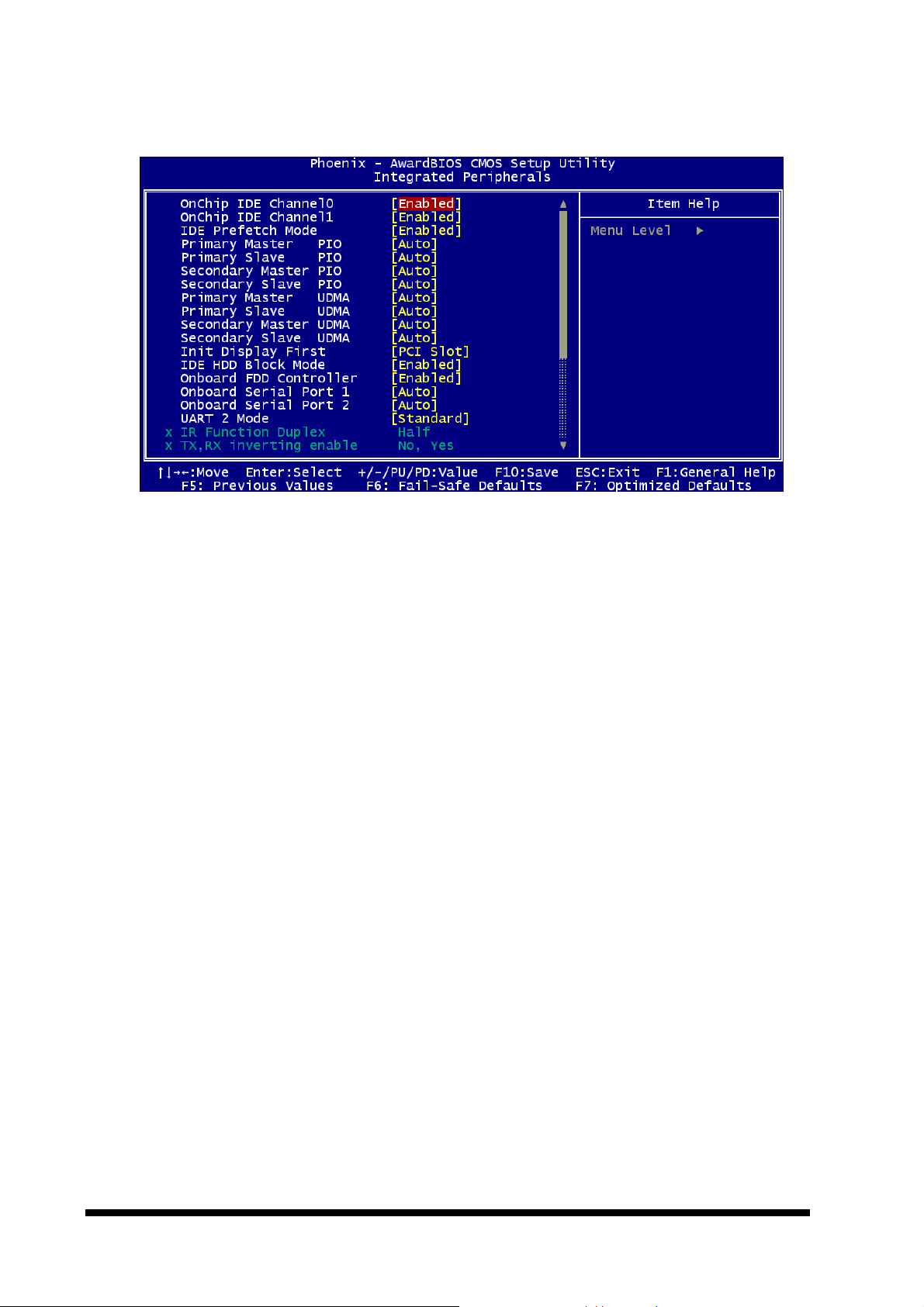
User’s Manual
4.5.5 Integrated Peripherals
4.5.5.1 OnChip IDE Channel 0
The chipset contains a PCI IDE interface with support for two IDE channels. Select
Enabled to activate the primary IDE interface. Select Disabled to deactivate this interface.
The choice: Enabled, Disabled.
4.5.5.2 OnChip IDE Channel 1
The chipset contains a PCI IDE interface with support for two IDE channels. Select
Enabled to activate the secondary IDE interface. Select Disabled to deactivate this
interface.
The choice: Enabled, Disabled.
4.5.5.3 IDE Prefetch Mode
The onboard IDE drive interfaces supports IDE prefetching, for faster drive accesses. If
you install a primary and/or secondary add-in IDE interface, set this field to Disabled if the
interface does not support prefetching.
The choice: Enabled, Disabled.
4.5.5.4 Primary/Secondary Master/Slave PIO
The four IDE PIO (Programmed Input/Output) fields let you set a PIO mode (0-4) for each
of the four IDE devices that the onboard IDE interface supports. Modes 0 through 4
provide successively increased performance. In Auto mode, the system automatically
determines the best mode for each device.
The choice: Auto, Mode 0, Mode 1, Mode 2, Mode 3, or Mode 4.
62 ECM-3610/3610L User’s Manual
Page 75

ECM-3610/3610L
4.5.5.5 Primary/Secondary Master/Slave UDMA
Ultra DMA/33 implementation is possible only if your IDE hard drive supports it and the
operating environment includes a DMA driver (Windows 95 OSR2 or a third-party IDE bus
master driver). If your hard drive and your system software both support Ultra DMA/33,
select Auto to enable BIOS support.
The Choice: Auto, Disabled.
4.5.5.6 Init Display First
This item allows you to decide to active whether PCI Slot or AGP first.
The choice: PCI Slot, AGP.
4.5.5.7 IDE HDD Block Mode
Block mode is also called block transfer, multiple commands, or multiple sector read/write.
If your IDE hard drive supports block mode (most new drives do), select Enabled for
automatic detection of the optimal number of block read/writes per sector the drive can
support.
The Choice: Enabled, Disabled.
4.5.5.8 Onboard FDC Controller
Select Enabled if your system has a floppy disk controller (FDC) installed on the system
board and you wish to use it. If you install and-in FDC or the system has no floppy drive,
select Disabled in this field.
The Choice: Enabled, Disabled.
4.5.5.9 Onboard Serial Port 1/Port2
Select an address and corresponding interrupt for the first and second serial ports.
The choice: 3F8/IRQ4, 2E8/IRQ3, 3E8/IRQ4, 2F8/IRQ3, Disabled, Auto.
4.5.5.10 UART 2 Mode
Select UART 2 mode as standard serial port or IR port.
The choice: Standard, ASKIR, HPSIR.
4.5.5.11 IR Function Duplex
Select the value required by the IR device connected to the IR port. Full-duplex mode
permits simultaneous two-direction transmission. Half-duplex mode permits transmission
in one direction only at a time.
The Choice: Half, Full.
ECM-3610/3610L User’s Manual 63
Page 76

User’s Manual
4.5.5.12 TX, RX Inverting Enable
This item allows you to determine the active of RxD, TxD level.
The Choice: Yes, No No, Yes No, No Yes, Yes
4.5.5.13 Onboard Parallel Port
Select a logical LPT port name and matching address for the physical parallel (printer)
port.
The choice: 378H/IRQ7, 278H/IRQ5, 3BCH/IRQ7, Floppy, Disabled.
4.5.5.14 Onboard Parallel Mode
Select an operating mode for the onboard parallel port. Select Compatible or Extended
unless you are certain both your hardware and software support EPP or ECP mode.
The choice: EPP, ECP, ECP/EPP, Normal,
4.5.5.15 ECP Mode Use DMA
Select a DMA channel for the port.
The choice: 3, 1.
4.5.5.16 Parallel Port EPP Type
Select EPP port type 1.7 or 1.9.
The choice: EPP1.7, EPP1.9.
4.5.5.17 Onboard Legacy Audio
This item allows you to enable or disable the onboard legacy audio function.
The choice: Enable, Disable.
4.5.5.18 Sound Blaster
This item allows you to enable or disable the onboard audio function is compatible with
sound blaster mode.
The choice: Enable, Disable.
4.5.5.19 SB I/O Base Address
This chipset traps I/O accesses for Sound Blaster compatibility at 220H, 240H, 260H, or
280H.
The choice: 220H, 240H, 260H, 280H.
64 ECM-3610/3610L User’s Manual
Page 77

ECM-3610/3610L
4.5.5.20 SB IRQ Select
Select an interrupt for the audio port.
The choice: IRQ 5, IRQ 7, IRQ 9, IRQ 10.
4.5.5.21 SB DMA Select
This chipset supports I/O trapping for DMA accesses and allows you to select the Audio
DMA type.
The choice: DMA 0, DMA 1, DMA 2, DMA 3.
4.5.5.22 MPU-401
This item allows you to enable or disable MPU-401 function.
The choice: Enable, Disable.
4.5.5.23 MPU-401 I/O Base Address
This chipset traps I/O accesses for ROLAND MPU 401 UART interface at 330H, 300H, or
Disable.
The choice: 300-303H, 310-313H, 320-323H, 330-333H.
ECM-3610/3610L User’s Manual 65
Page 78
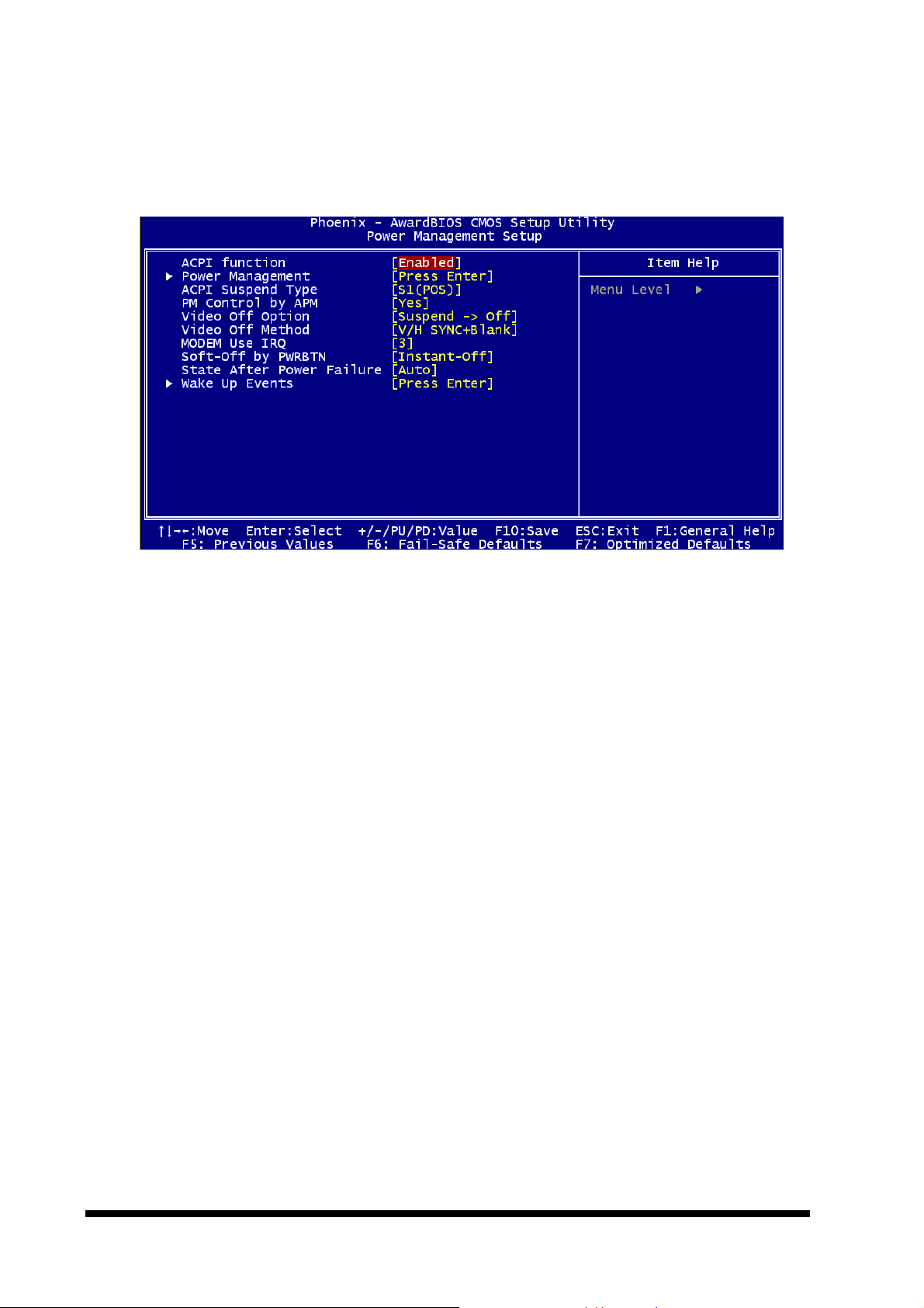
User’s Manual
4.5.6 Power Management Setup
The Power Management Setup allows you to configure you system to most effectively
save energy while operating in a manner consistent with your own style of computer use.
4.5.6.1 ACPI Function
This item allows you to enable/disable the ACPI function.
The choice: Enable, Disable.
66 ECM-3610/3610L User’s Manual
Page 79
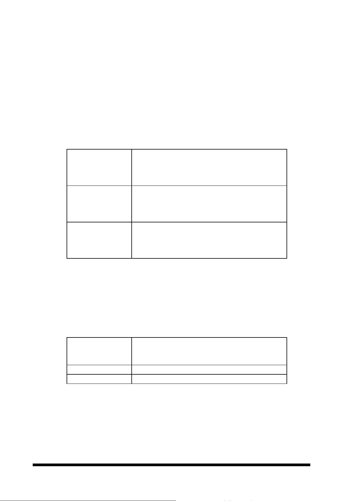
ECM-3610/3610L
4.5.6.2 Power Management
This category allows you to select the type (or degree) of power saving and is directly
related to the following modes:
1. HDD Power Down
2. Doze Mode
3. Suspend Mode
There are three selections for Power Management , both of them have fixed mode
settings.
Min. Power Saving Minimum power management ,
HDD Power Down = Disabled,
Doze Mode = 1 Hour
Suspend Mode = 1 Hour
Max. Power Saving Maximum power management,
HDD Power Down = Disabled,
Doze Mode = 1 Min
Suspend Mode = 1 Min
User Defined Allows you to set each mode individually. When not
disabled, each of the ranges are from 1 min. to 1 hr.
except for HDD Power Down which ranges from 1 min.
to 15 min. and disable.
4.5.6.3 PM Control by APM
This item allows you to enable/disable the Advanced Power Management (APM) function.
The choice: Yes, No.
4.5.6.4 Video Off Method
This determines the manner in which the monitor is blanked.
V/H SYNC+Blank This selection will cause the system to turn off the
vertical and horizontal synchronization ports and write
blanks to the video buffer.
Blank Screen This option only writes blanks to the video buffer.
DPMS Initial display power management signaling.
4.5.6.5 MODEM Use IRQ
This determines the IRQ in which the MODEM can use.
The choice: 3, 4, 5, 7, 9, 10, 11, or NA.
ECM-3610/3610L User’s Manual 67
Page 80

User’s Manual
4.5.6.6 Soft-Off by PWRBTN
Pressing the power button for more than 4 seconds forces the system to enter the Soft-Off
state when the system has “hung”.(Only could working on ATX Power supply)
The choice: Delay 4 Sec, Instant-Off.
4.5.6.7 Wake up Events
PM Wake up events are I/O events whose occurrence can prevent the system from
entering a power saving mode or can awaken the system from such a mode. In effect, the
system remains alert for anything which occurs to a device which is configured as On,
even when the system is in a power down mode.
4.5.6.7.1 VGA
When ON, your can set the LAN awakens the system.
4.5.6.7.2 LPT & COM
When select LPT/COM, any activity from one of the listed system peripheral devices or
IRQs wakes up the system.
4.5.6.7.3 HDD & FDD
When On of HDD & FDD, any activity from one of the listed system peripheral devices
wakes up the system.
4.5.6.7.4 PCI Master
When you are On of PCI Master, any activity from one of the list system peripheral
devices wakes up the system.
4.5.6.8 Power On by PCI Card
This item allows you to determine that does any activity from one of the list system
peripheral devices wakes up the system.
The Choice. Enable, Disabled.
4.5.6.8.1 Modem Ring Resume
An input signal on the serial Ring Indicator (RI) line (in other words, an incoming call on
the modem) awakens the system from a soft off state.
4.5.6.8.2 DisableRTC Alarm Function
When Enabled, your can set the date and time at which the RTC (real-time clock) alarm
awakens the system from Suspend mode.
68 ECM-3610/3610L User’s Manual
Page 81
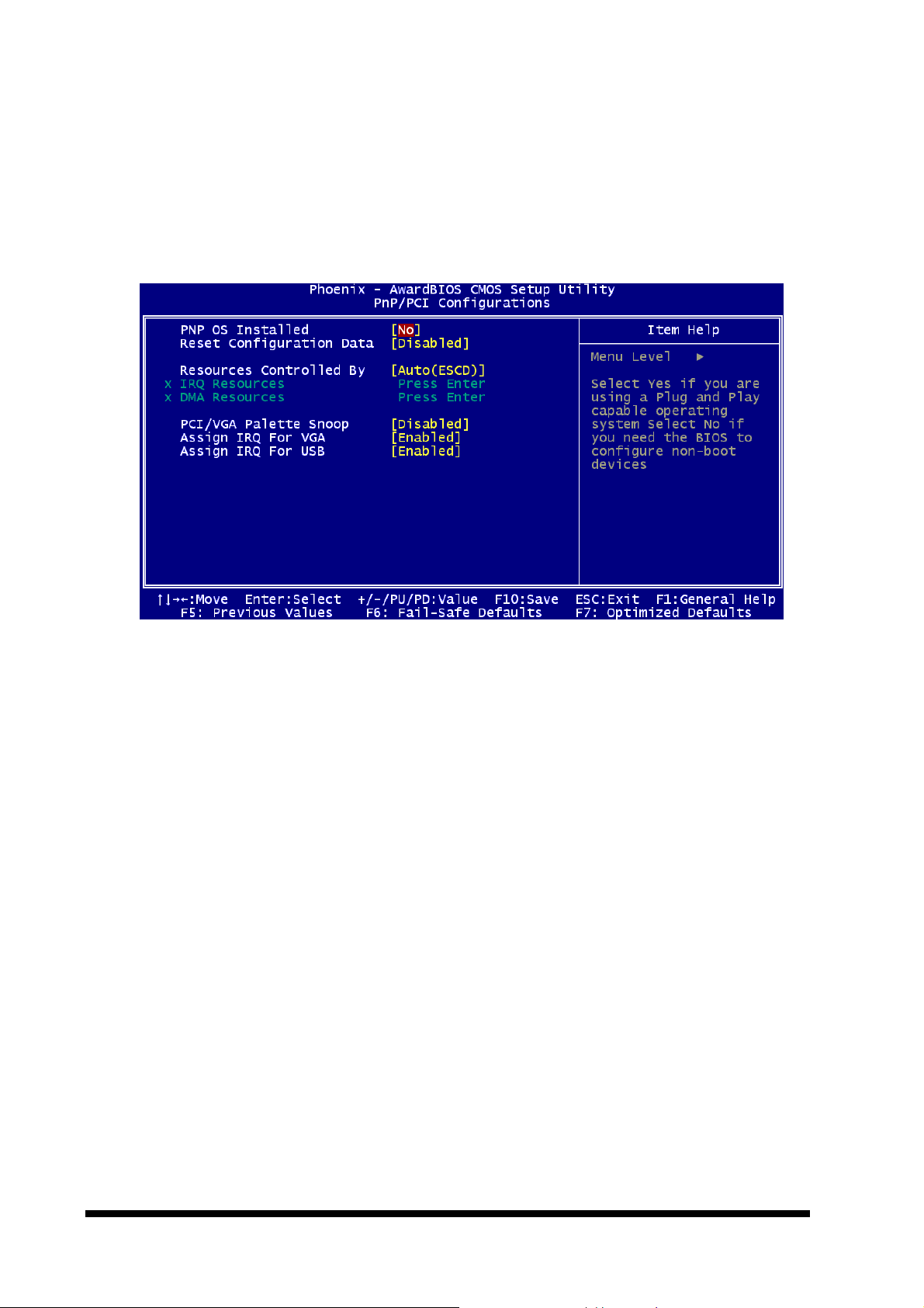
ECM-3610/3610L
4.5.7 PnP/PCI Configuration Setup
This section describes configuring the PCI bus system. PCI, or Personal Computer
Interconnect, is a system which allows I/O devices to operate at speeds nearing the speed
the CPU itself uses when communicating with its own special components. This section
covers some very technical items and it is strongly recommended that only experienced
users should make any changes to the default settings.
4.5.7.1 PnP OS Installed
This item allows you to determine install PnP OS or not.
The choice: Yes, No.
4.5.7.2 Reset Configuration Data
Normally, you leave this field Disabled. Select Enabled to reset Extended System
Configuration Data (ESCD) when you exit Setup if you have installed a new add-on and
the system reconfiguration has caused such a serious conflict that the operating system
cannot boot.
The choice: Enabled, Disabled.
4.5.7.3 Resource Controlled by
The Award Plug and Play BIOS has the capacity to automatically configure all of the boot
and Plug and Play compatible devices. However, this capability means absolutely nothing
unless you are using a Plug and Play operating system such as Windows95. If you set
this field to “manual” choose specific resources by going into each of the sub menu that
follows this field (a sub menu is preceded by a “Ø”).
The choice: Auto, Manual.
ECM-3610/3610L User’s Manual 69
Page 82

User’s Manual
4.5.7.4 IRQ Resources
When resources are controlled manually, assign each system interrupt a type, depending
on the type of device using the interrupt.
4.5.7.5 IRQ3/4/5/7/9/10/11/12/14/15 Assigned to
This item allows you to determine the IRQ assigned to the ISA bus and is not available to
any PCI slot. Legacy ISA for devices compliant with the original PC AT bus specification,
PCI/ISA PnP for devices compliant with the Plug and Play standard whether designed for
PCI or ISA bus architecture.
The Choice: Legacy ISA and PCI/ISA PnP.
4.5.7.6 DMA Resources
When resources are controlled manually, assign each system DMA channel a type,
depending on the type of device using the DMA channel.
4.5.7.7 DMA 0/1/3/5/6/7 Assigned to
Legacy ISA for devices compliant with the original PC AT bus specification, PCI/ISA PnP
for devices compliant with the Plug and Play standard whether designed for PCI or ISA
bus architecture.
Choices are Legacy ISA and PCI/ISA PnP.
4.5.7.8 PCI / VGA Palette Snoop
Leave this field at Disabled.
Choices are Enabled, Disabled.
4.5.7.9 Assign IRQ for VGA
This item allows you to Enable or Disable assign an IRQ for onboard VGA controller.
The Choices : Enabled, Disabled.
4.5.7.10 Assign IRQ for USB
This item allows you to Enable or Disable assign an IRQ for onboard USB Controller.
The Choices : Enabled, Disabled.
70 ECM-3610/3610L User’s Manual
Page 83
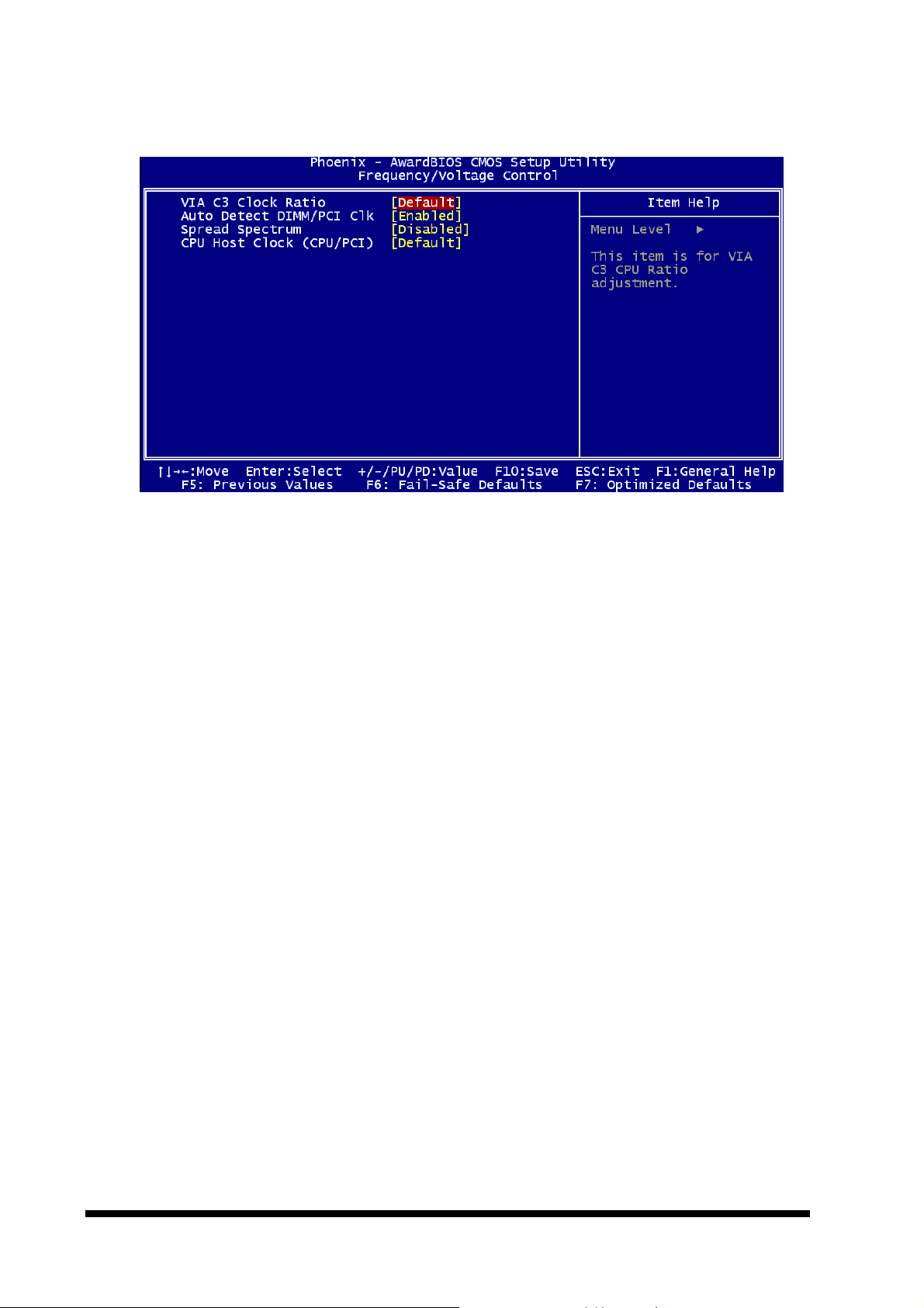
4.5.8 Frequency / Voltage Control
4.5.8.1 VIA C3 Clock Ratio
ECM-3610/3610L
This item allows you to select the VIA C3 CPU clock ratio.
4.5.8.2 Auto Detect DIMM/ PCI Clk
This item allows you to enable/disable auto detect DIMM/PCI Clock.
The choice: Enable, Disable.
4.5.8.3 Spread Spectrum
This item allows you to enabled Spread Spectrum Modulated.
The choice: Enable, Disable.
4.5.8.4 CPU Host Clock (CPU / PCI)
This item allows you to select the CPU host clock frequency.
ECM-3610/3610L User’s Manual 71
Page 84
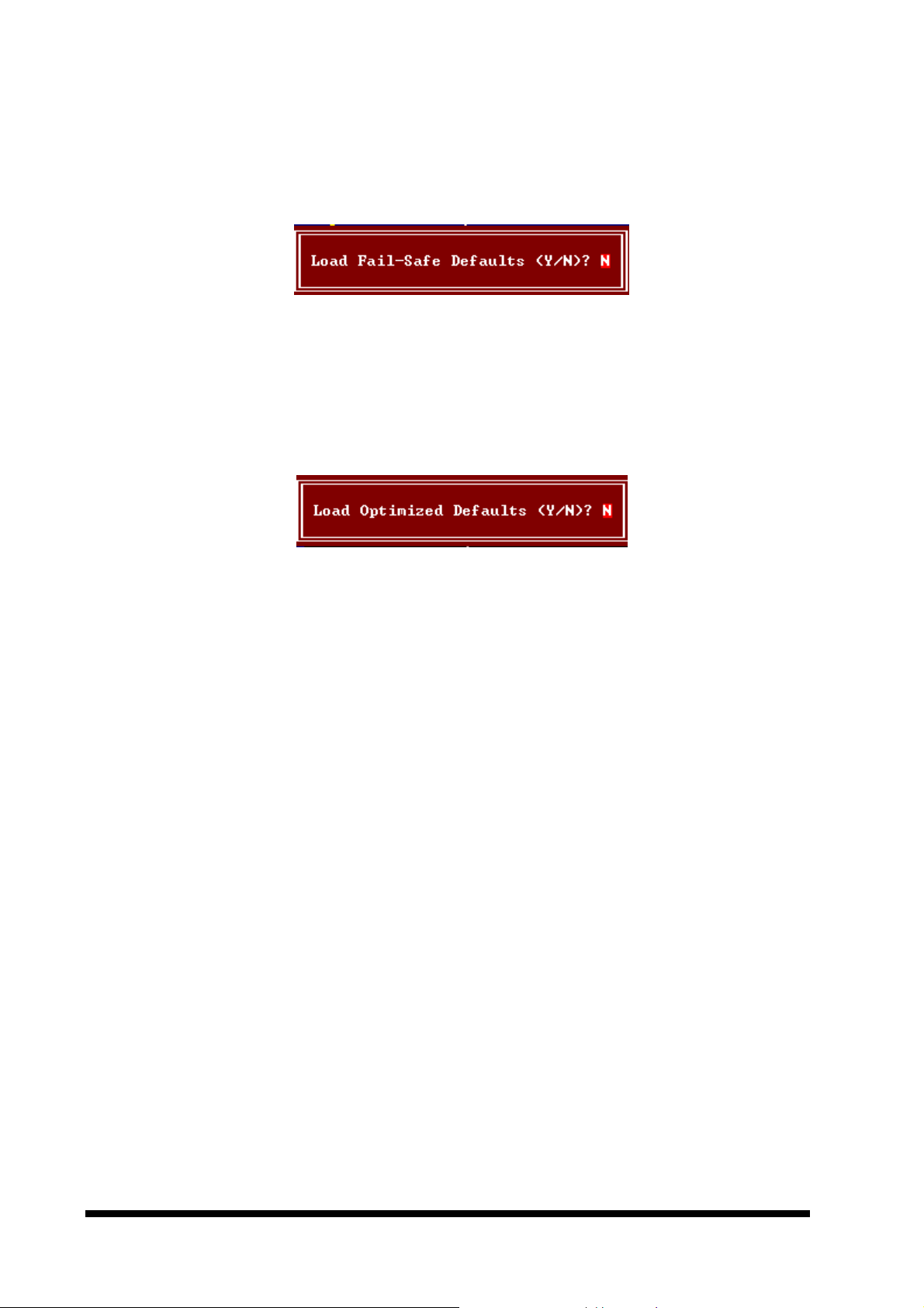
User’s Manual
4.5.9 Load Fail-Safe Defaults
When you press <Enter> on this item you get a confirmation dialog box with a message
similar to:
Pressing ‘Y’ loads the BIOS default values for the most stable, minimal-performance
system operations.
4.5.10 Load Optimized Defaults
When you press <Enter> on this item you get a confirmation dialog box with a message
similar to:
Pressing ‘Y’ loads the default values that are factory settings for optimal performance
system operations.
72 ECM-3610/3610L User’s Manual
Page 85
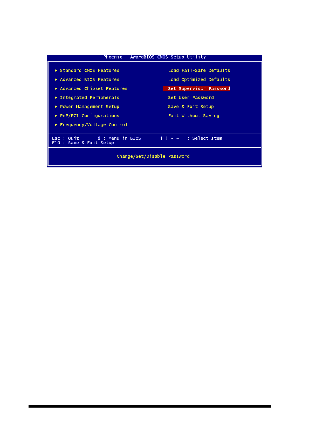
ECM-3610/3610L
4.5.11 Supervisor / User Password Setting
You can set either supervisor or user password, or both of them. The differences between
are:
supervisor password: can enter and change the options of the setup menus.
user password: just can only enter but do not have the right to change the options of the
setup menus. When you select this function, the following message will appear at the
center of the screen to assist you in creating a password.
ENTER PASSWORD:
Type the password, up to eight characters in length, and press <Enter>. The password
typed now will clear any previously entered password from CMOS memory. You will be
asked to confirm the password. Type the password again and press <Enter>. You may
also press <Esc> to abort the selection and not enter a password. To disable a password,
just press <Enter> when you are prompted to enter the password. A message will confirm
the password will be disabled. Once the password is disabled, the system will boot and
you can enter Setup freely.
PASSWORD DISABLED.
When a password has been enabled, you will be prompted to enter it every time you try to
enter Setup. This prevents an unauthorized person from changing any part of your system
configuration. Additionally, when a password is enabled, you can also require the BIOS to
request a password every time your system is rebooted. This would prevent unauthorized
use of your computer. You determine when the password is required within the BIOS
Features Setup Menu and its Security option (see Section 3). If the Security option is set
to “System”, the password will be required both at boot and at entry to Setup. If set to
“Setup”, prompting only occurs when trying to enter Setup.
ECM-3610/3610L User’s Manual 73
Page 86
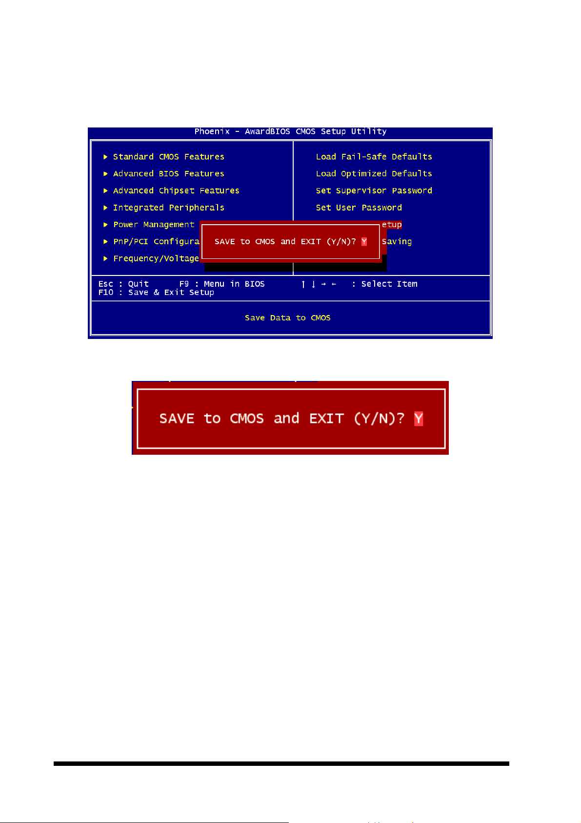
User’s Manual
4.5.12 Exit Selecting
4.5.12.1 Save & Exit Setup
Pressing <Enter> on this item asks for confirmation:
Pressing “Y” stores the selections made in the menus in CMOS – a special section of
memory that stays on after you turn your system off. The next time you boot your
computer, the BIOS configures your system according to the Setup selections stored in
CMOS. After saving the values the system is restarted again.
74 ECM-3610/3610L User’s Manual
Page 87
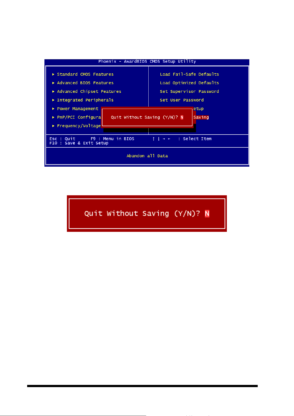
4.5.12.2 Exit Without Saving
ECM-3610/3610L
Pressing <Enter> on this item asks for confirmation:
This allows you to exit Setup without storing in CMOS any change. The previous
selections remain in effect. This exits the Setup utility and restarts your computer.
ECM-3610/3610L User’s Manual 75
Page 88
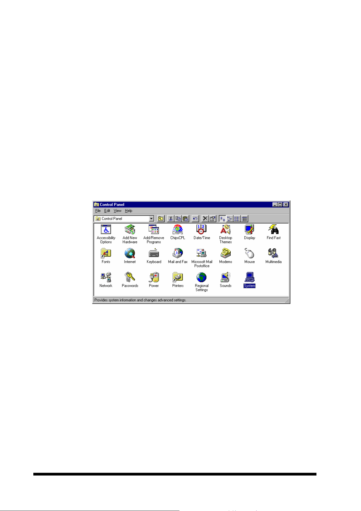
User’s Manual
5. Driver Installation
5.1 Driver Installation for Ethernet Adapter
5.1.1 Windows 9x Ethernet Installation
The best way to install the driver for the Ethernet controller is to use the plug and play
system of Windows 9x. The following procedures illustrate how the installation can be
done.
1. If a driver for the Ethernet controller is already installed this must be removed first.
This can be done by the following steps shown below.
• Click the ‘Start’ button, click on ‘Settings’ and on ‘Control panel’ to open the
control panel.
Your display should now look as below (possibly with different size and icons):
• Double click the ‘System’ icon (highlighted above).
• Select the ‘Device Manager’ tab.
76 ECM-3610/3610L User’s Manual
Page 89
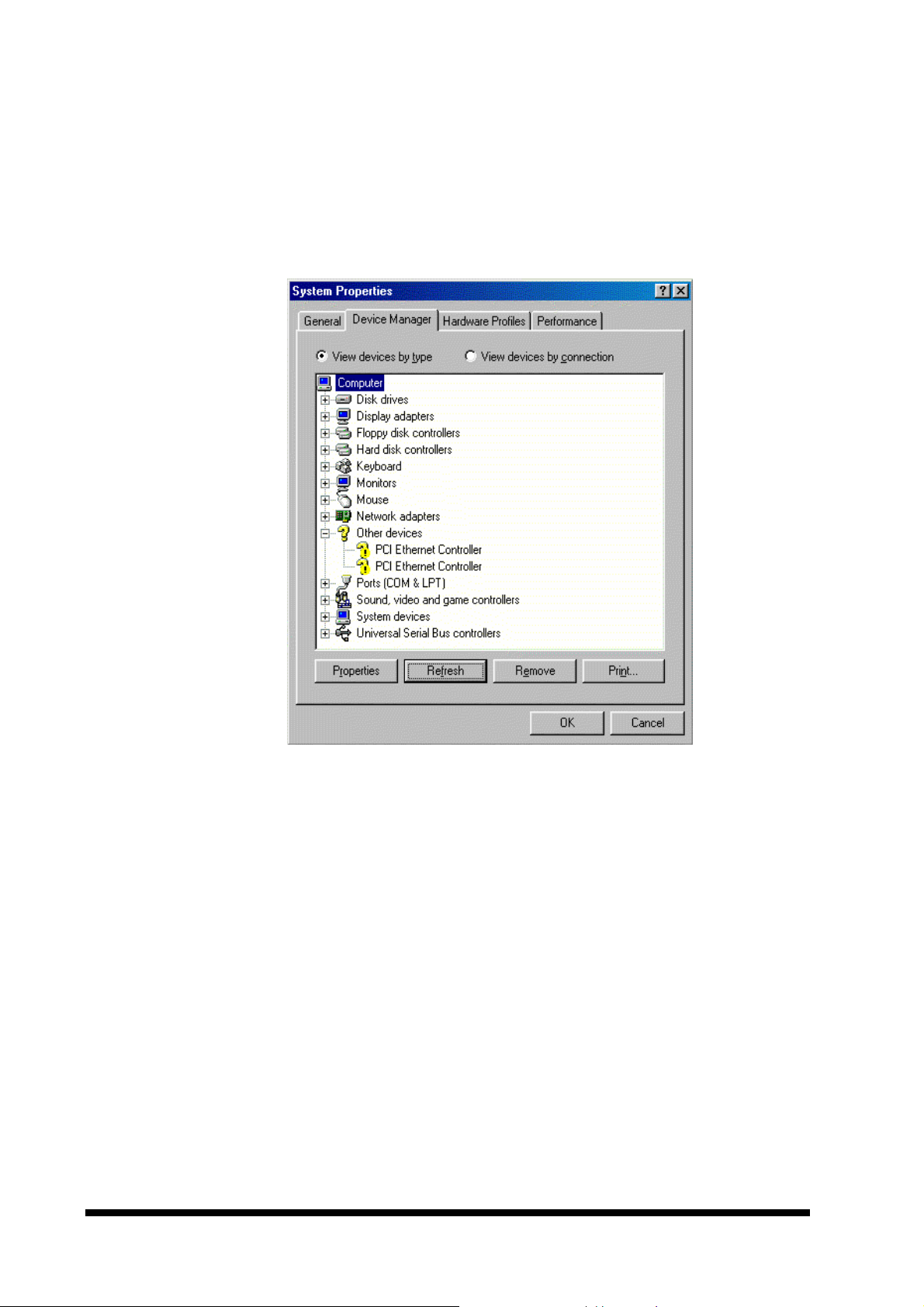
ECM-3610/3610L
• If the ‘Network adapters’ line is present, expand the line and remove the PCI
Ethernet Controller adapters. This is done by selecting the line and clicking the
‘Remove’ button.
Before removal of the adapter(s), your screen might look like this:
• When all adapters are removed (or none were present), a new driver can be
installed.
2. Reboot the computer.
ECM-3610/3610L User’s Manual 77
Page 90
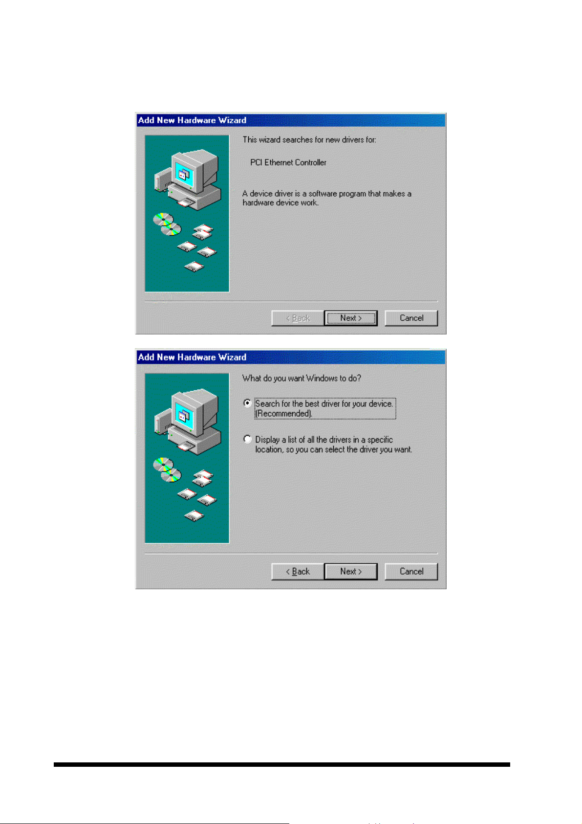
User’s Manual
3. During the boot the network adapter should be detected as shown below:
.
78 ECM-3610/3610L User’s Manual
Page 91
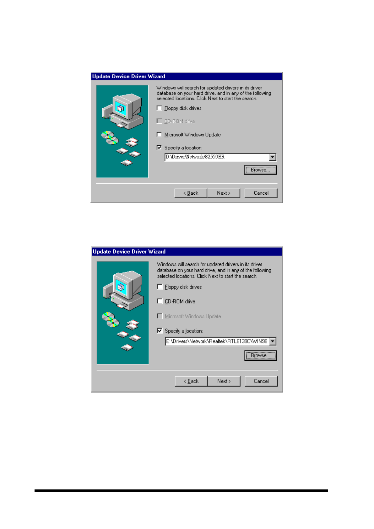
4. Specify the location of network adapter and click ‘Next’ (see below).
.
ECM-3610/3610L
If your CPU board using Realtek RTL8139C Network chip, the location of network
adapter is shown as below
.
ECM-3610/3610L User’s Manual 79
Page 92
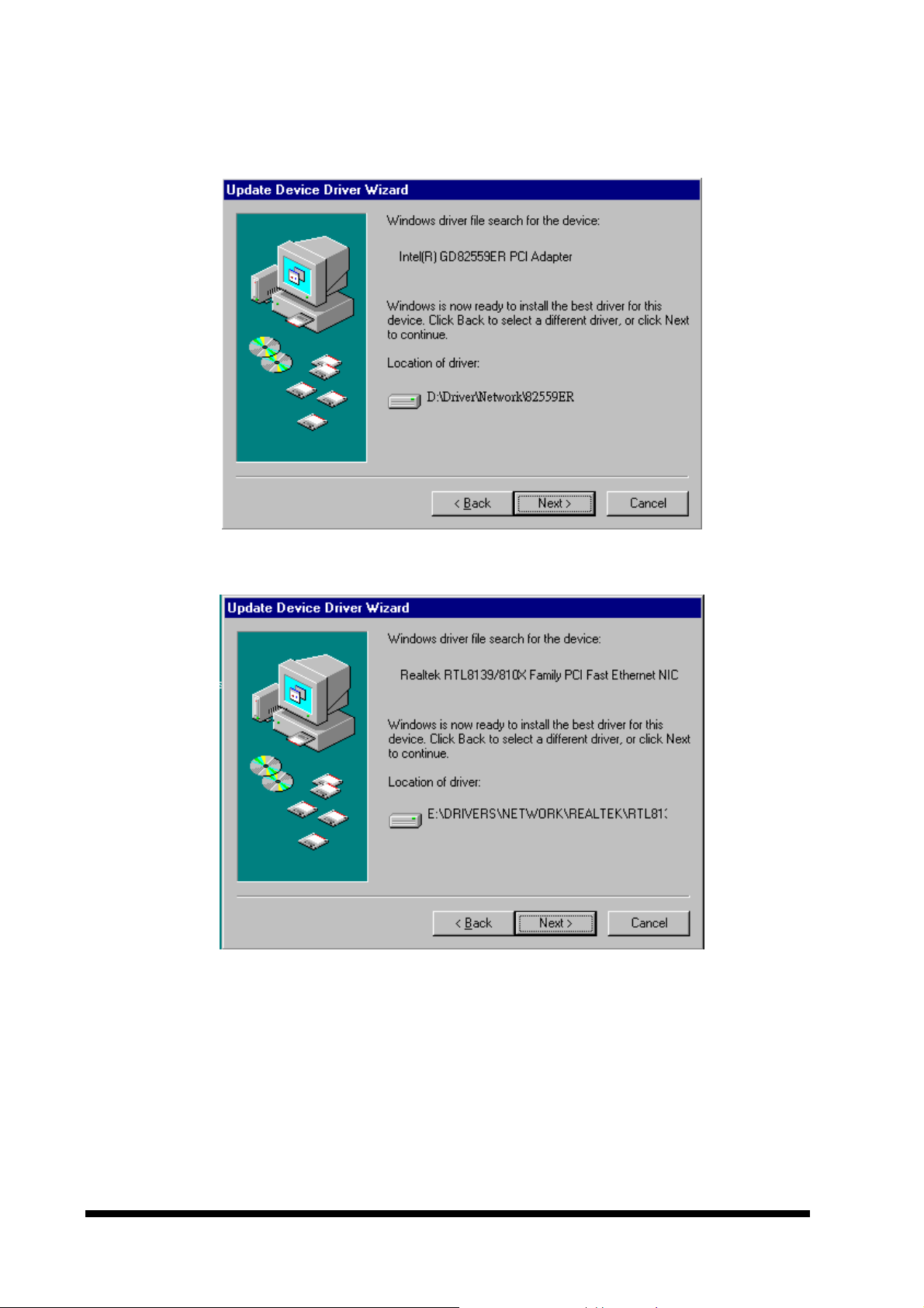
User’s Manual
5. Click the ‘Next’ button.
.
or
80 ECM-3610/3610L User’s Manual
Page 93
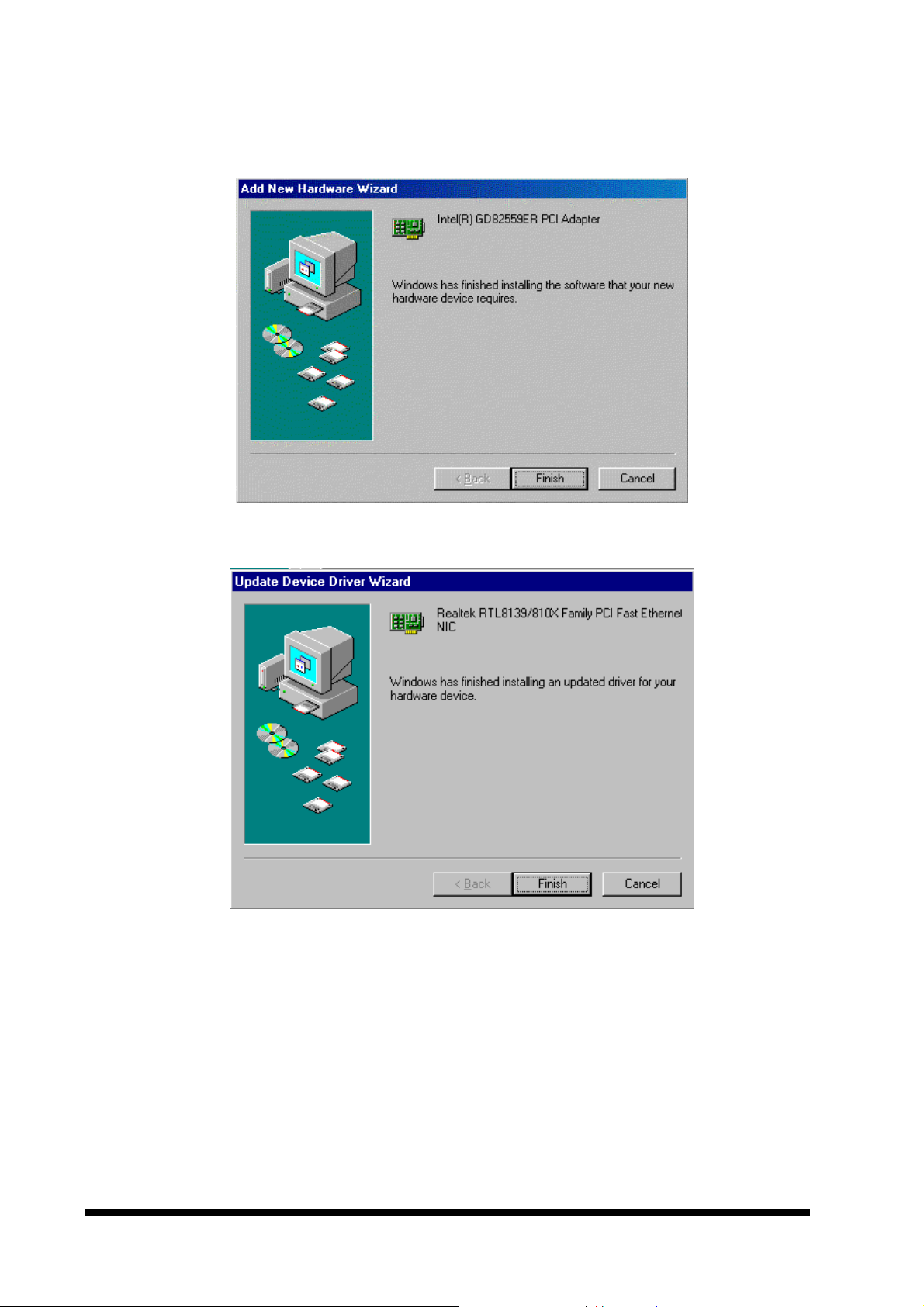
6. Click the ‘Finish’ button.
.
ECM-3610/3610L
or
7. Depending on the configuration, a request for the windows disks or CD-ROM may be
necessary. Insert the disk / CD-ROM and click the ‘OK’ button. An entry of the
directory for the files may then be required. After typing the path name, click the ‘OK’
button.
ECM-3610/3610L User’s Manual 81
Page 94
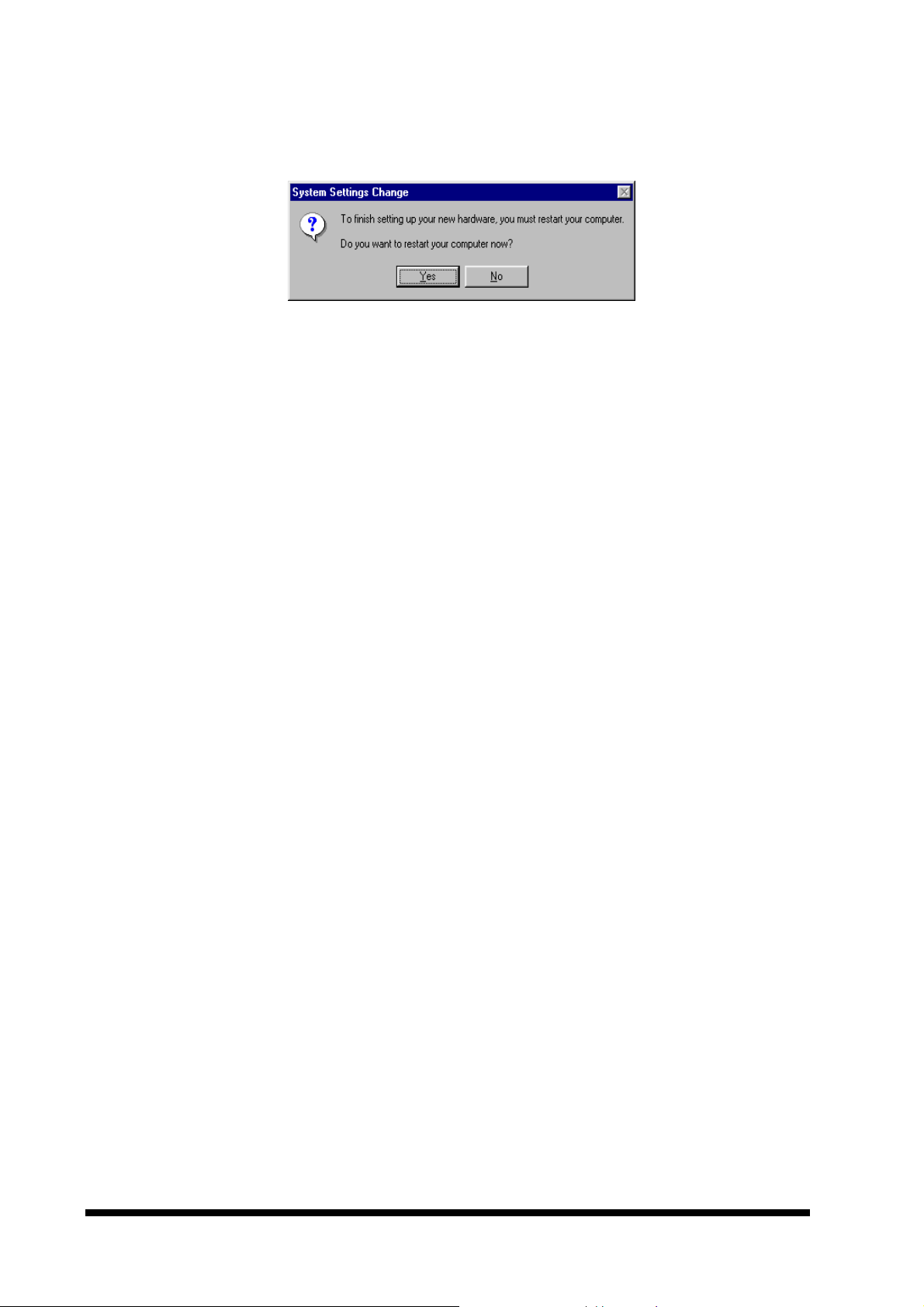
User’s Manual
8. To complete the installation, reboot the computer by clicking the ‘Yes’ button in the
window shown below.
9. After the system restarts, the network adapter should be installed. Protocols, clients
etc. may now be installed for the network in use.
Further configuration of the adapter may be made in the ‘Advanced’ section of the driver
properties. These options may be accessed through the ‘Network’ icon in the control
panel (Select the network adapter, click the ‘Properties’ button and select the ‘Advanced’
tab).
82 ECM-3610/3610L User’s Manual
Page 95
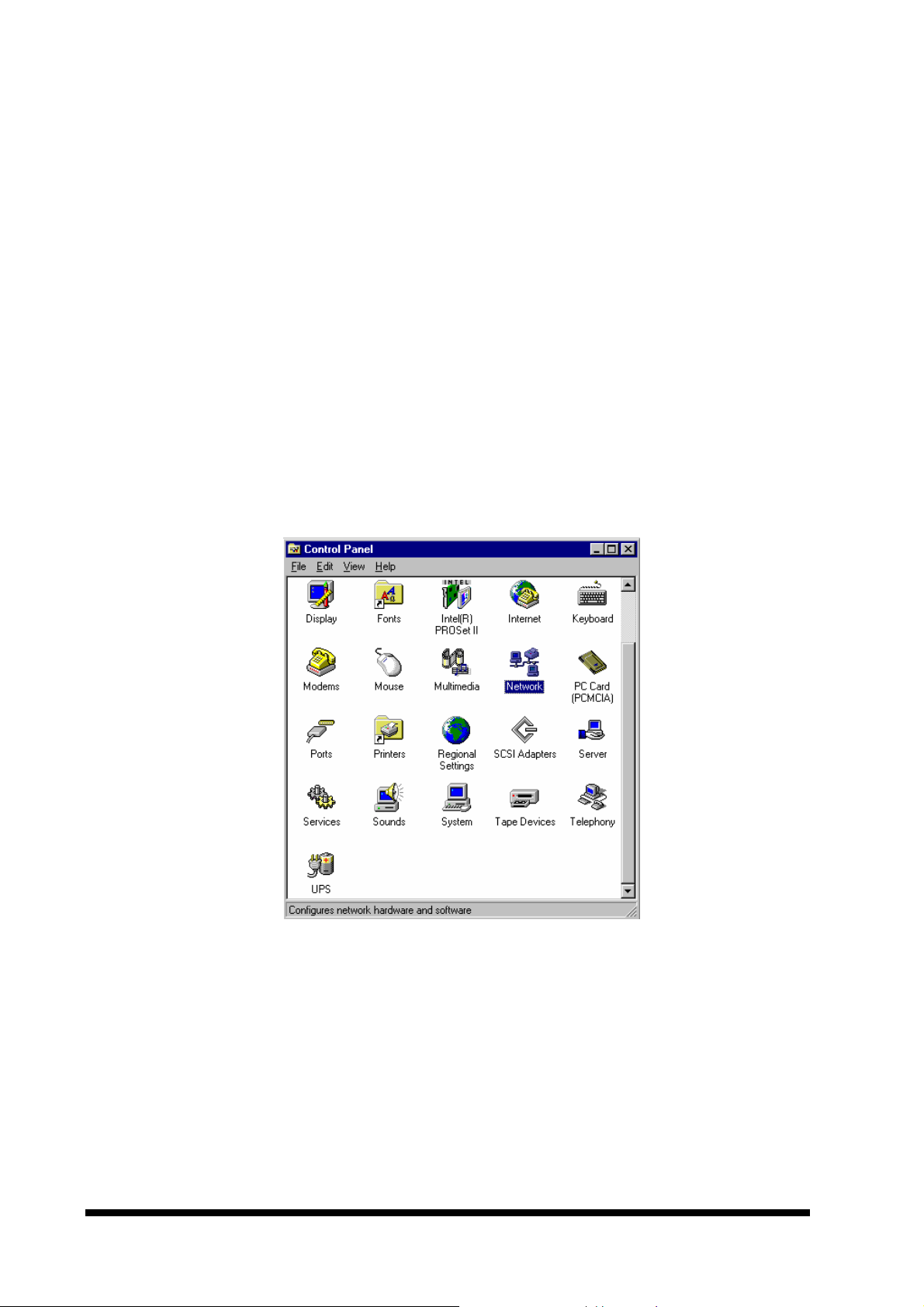
ECM-3610/3610L
5.1.2 Windows NT 4.0 Ethernet Installation
A driver for the Intel 82559ER or Realtek RTL8139C Ethernet controller on board is
included in the attached supporting CD-ROM. The driver for these adapters are
denoted ’Intel GD82559ER PCI Adapter’ or ’Realtek RTL8139(A/B/C) PCI Fast Ethernet
Adapter’. The driver may be installed in two ways:
• During the installation process where the network may be configured as an integrated
part. In this case the adapter may be chosen or auto-detected when the network
adapter is to be installed.
• In the network settings after Windows NT 4.0 is installed.
The following procedures describe the steps to install the Network adapter driver on
Windows NT 4.0.
1. Click the ‘Start’ button on the task bar. Select ‘Settings’ and ‘Control Panel’ to start the
control panel shown below:
ECM-3610/3610L User’s Manual 83
Page 96
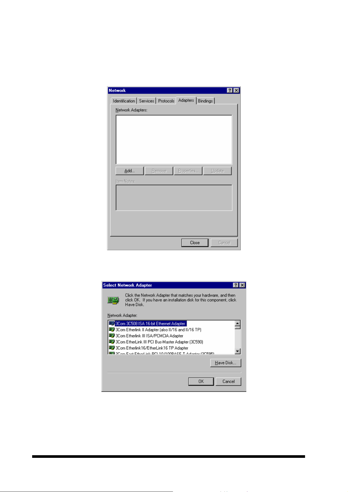
User’s Manual
2. Double click the ‘Network’ icon and then click the ‘Adapters’ tab on the following
window. A window as the one shown below should now appear.
3. Click the ‘Add...’ button, and the following window should appear.
4. Click the ‘Have Disk… ’ button to install the Network adapter driver from CD-ROM. A
window as the one shown below should now appear.
84 ECM-3610/3610L User’s Manual
Page 97
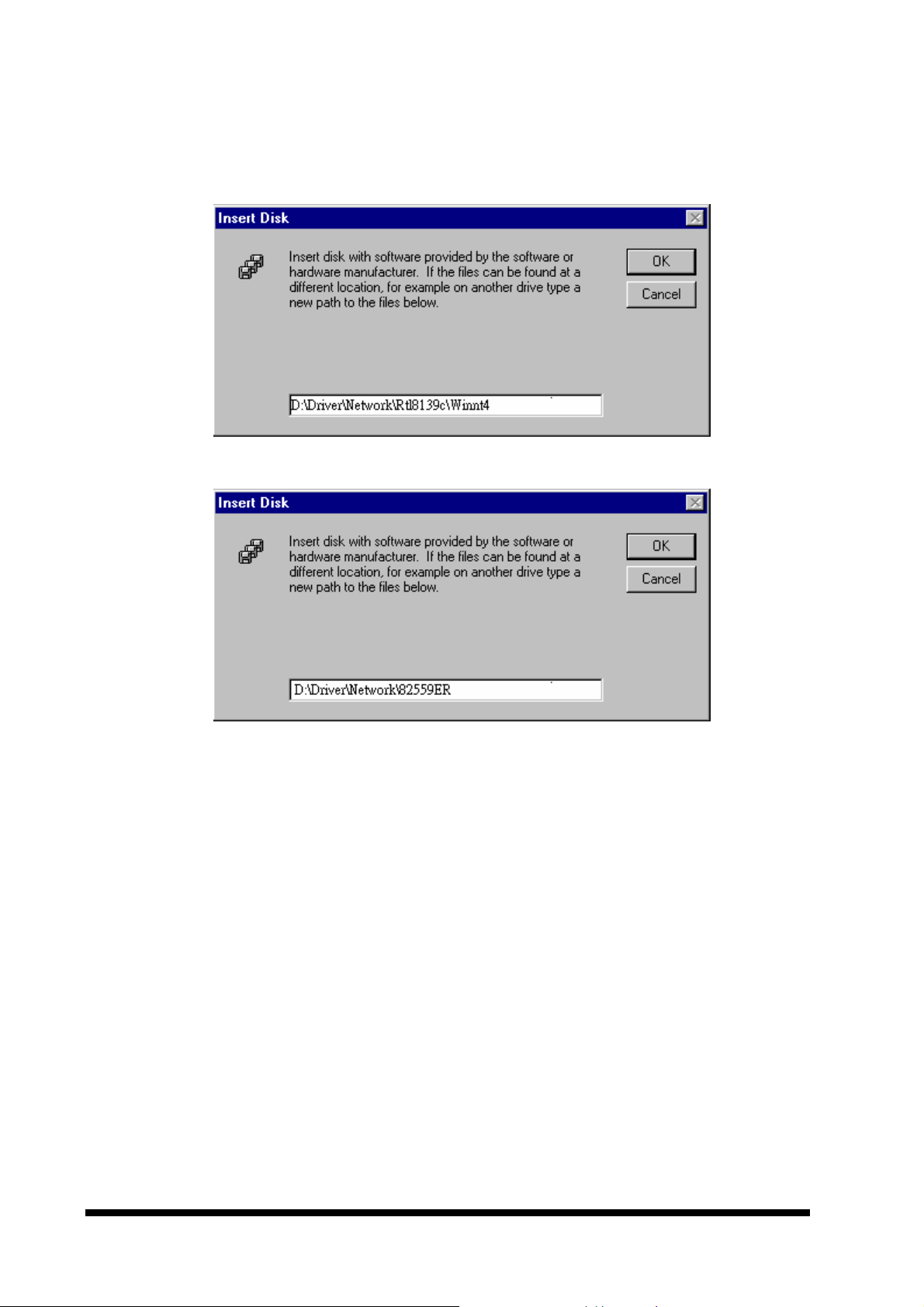
5. Locate the path of Network adapter driver and click the ‘OK’ button.
or
ECM-3610/3610L
ECM-3610/3610L User’s Manual 85
Page 98
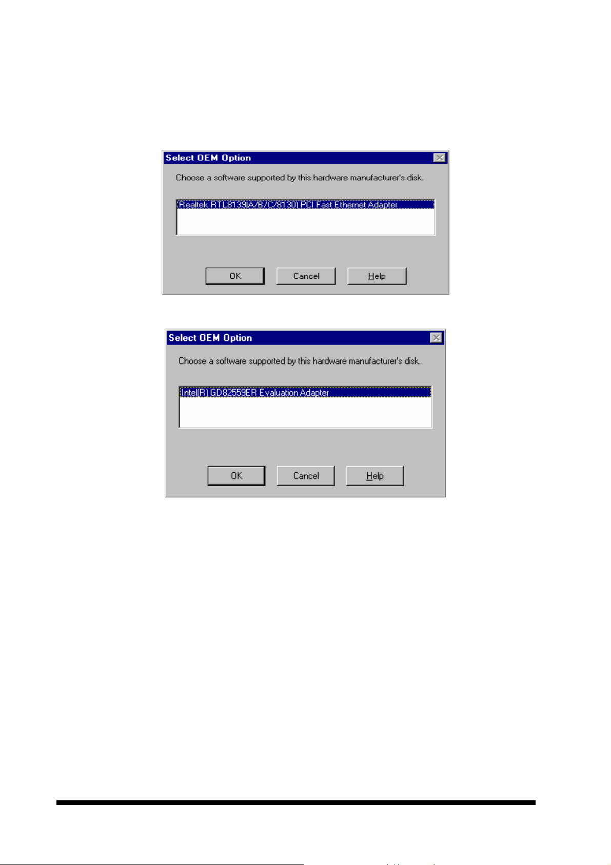
User’s Manual
6. Select the ‘Realtek RTL8139(A/B/C) PCI Fast Ethernet Adapter’ or ‘Intel GD82559ER
Ethernet Adapter’ from the list (as shown below) and click the ‘OK’ button.
or
86 ECM-3610/3610L User’s Manual
Page 99
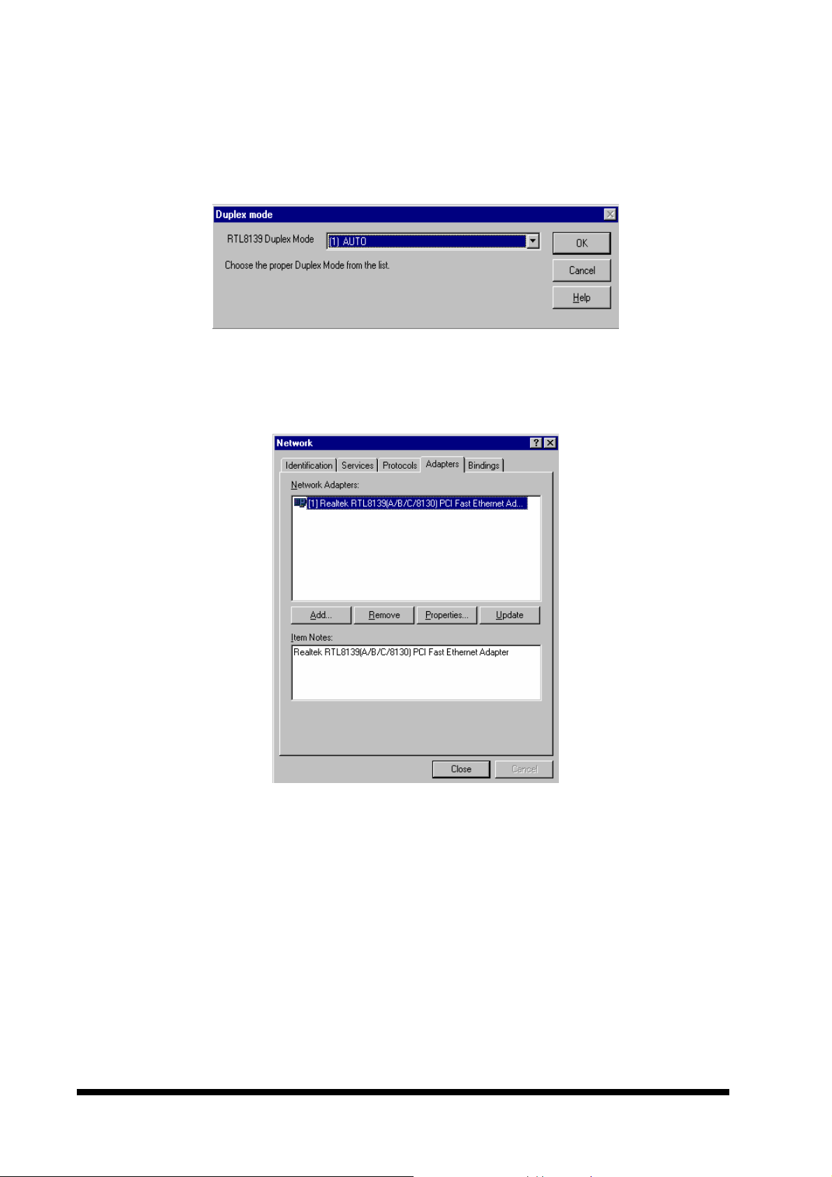
ECM-3610/3610L
7. If your hardware using Intel-82559ER Ethernet controller, please proceed to 12.
8. Select the ‘(1) Auto’ to set RTL8139C Ethernet controller to Auto Duplex Mode (as
shown below) and click the ‘OK’ button.
9. Click ‘Close’ to accept the settings.
ECM-3610/3610L User’s Manual 87
Page 100
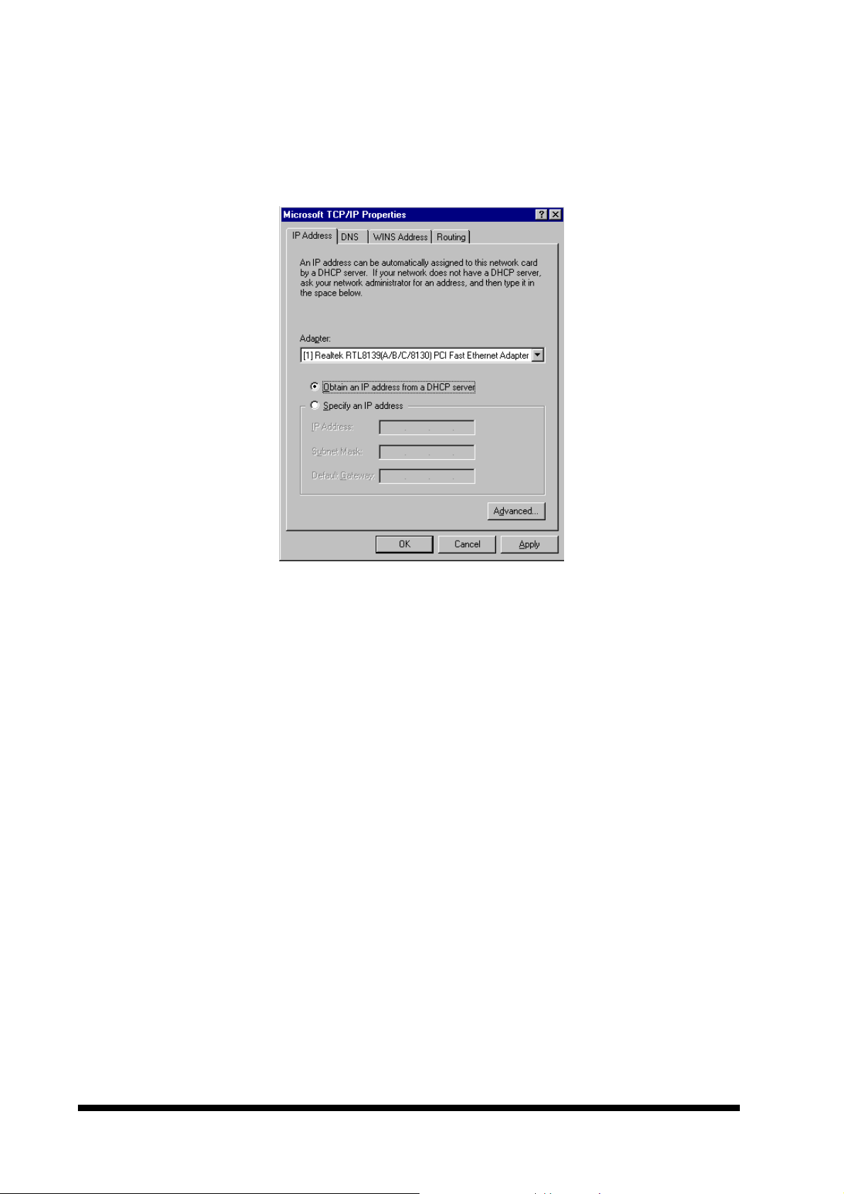
User’s Manual
10. Protocols, Services etc. may now be installed and configured for the network to be
used. An example is shown below.
11. If your hardware using Realtek RTL8139C Ethernet controller, please proceed to 17.
88 ECM-3610/3610L User’s Manual
 Loading...