ETRON EM566168 Datasheet

Etr onT ech
EM566168
1M x 16 Pseudo SRAM
Preliminary, Rev 0.2 Apr. 2002
Features
Organized as 1M words by 16 bits
•
Fast Cycle Time : 70ns
•
Standby Current : 100uA
•
Deep power-down Current : 10uA (Memory cell data
•
invalid)
Byte data control: LB# (DQ0 - 7), UB# (DQ8 - 15)
•
Compatible with low power SRAM
•
Single Power Supply Voltage : 3.0V±0.3V
•
Package Type : 48-ball FBGA, 6x8mm
•
Pin Description
Symbol
A0 – A19 Address Inputs
DQ0 – DQ15 Data Inputs/Outputs
CE1# Chip Enable
CE2 Deep Power Down
OE# Output Enable
WE# Write Control
LB# Lower Byte Control
UB# Upper Byte Control
VCC Power Supply
VSS Ground
Function
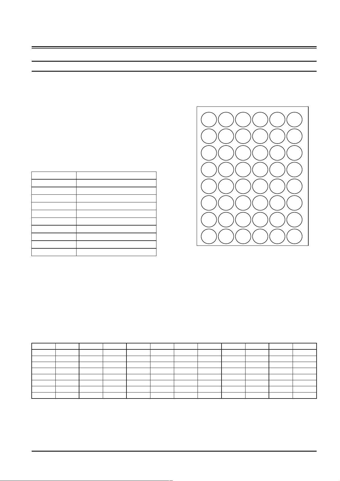
Pin Assignment 48-Ball BGA, Top View
6 5 4 3 2 1
A
B
C
D
E
F
G
H
LB# OE#
DQ8 UB#
DQ9 DQ10
VSS DQ11
VCC DQ12
DQ14 DQ13
DQ15 A19
A18 A8
A0 A1
A3 A4
A5 A6
A17 A7
NC A16
A14 A15
A12 A13
A9 A10
A2 CE2
CE1# DQ0
DQ1 DQ2
DQ3 VCC
DQ4 VSS
DQ5 DQ6
WE# DQ7
A11 NC
Overview
The EM566168 is a 16M-bit Pseudo SRAM organized as 1M words by 16 bits. It is designed with advanced
CMOS technology specified RAM featuring low power static RAM compatible function and pin configuration. This
device operates from a single power supply. Advanced circuit technology provides both high speed and low
power. It is automatically placed in low-power mode when CS1# or both UB# and LB# are asserted high or CS2
is asserted low. There are three control inputs. CS1# and CS2 are used to select the device, and output enable
(OE#) provides fast mem ory access. Data byte control pins (LB#,UB#) provide lower and upper byte access .
This device is well suited to various microprocessor system applications where high speed, low power and
battery backup are required. And, with a guaranteed wide operating range, the EM566168 can be used in
environments exhibiting extreme temperature conditions.
Pin Location
Symbol Location Symbol Location Symbol Location Symbol Location Symbol Location Symbol Location
A0 A3 A8 H2 A16 E4 DQ3 D5 DQ11 D2 WE# G5
A1 A4 A9 H3 A17 D3 DQ4 E5 DQ12 E2 LB# A1
A2 A5 A10 H4 A18 H1 DQ5 F5 DQ13 F2 UB# B2
A3 B3 A11 H5 A19 G2 DQ6 F6 DQ14 F1 VCC D6
A4 B4 A12 G3 NC H6 DQ7 G6 DQ15 G1 VCC E1
A5 C3 A13 G4 DQ0 B6 DQ8 B1 CE1# B5 GND D1
A6 C4 A14 F3 DQ1 C5 DQ9 C1 CE2 A6 GND E6
A7 D4 A15 F4 DQ2 C6 DQ10 C2 OE# A2 NC E3
Etron Technology, Inc.
No. 6, Technology Rd. V, Science-Based Industrial Park, Hsinchu, Taiwan 30077, R.O.C.
TEL: (886)-3-5782345 FAX: (886)-3-5778671
Etron Technology, Inc., reserves the right to make changes to its products and specifications without notice.

Etr onT ech
R
C
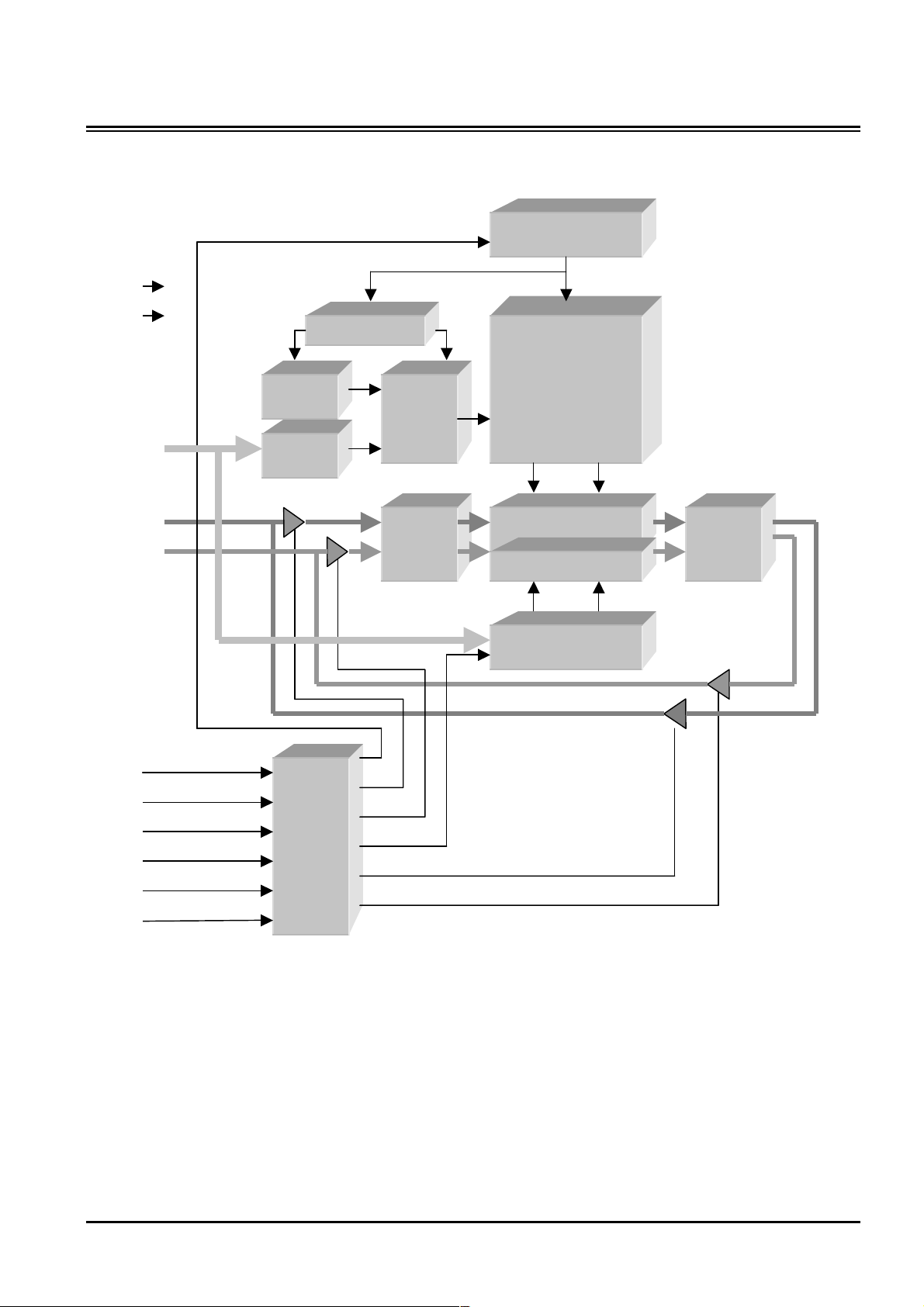
Block Diagram
VCC
EM566168
Standby/Deep Power
Down Mode Control
VSS
A0 – A19
DQ0 – DQ7
DQ8 – DQ15
efresh
ounter
Address
Buffer
Refresh Control
Address
Decoder
Control
Row
Input
Data
Memory Cell Array
1M x 16
Sense AMP
Column Decoder
Address Buffer
Output
Data
Control
CS1#
CS2
OE#
WE#
LB#
UB#
Control
Logic
Preliminary 2 Rev 0.2
Feb. 2002

Etr onT ech
EM566168
Operating Mode
CS1# CS2 OE# WE# LB# UB# DQ0~DQ7 DQ8~DQ15 Mode Power
H H X X X X High-Z High-Z Deselect Standby
X L X X X X High-Z High-Z Deselect Deep Power Down
L H X X H H High-Z High-Z Deselect Standby
L H H H L X High-Z High-Z Output Disabled Active
L H H H X L High-Z High-Z Output Disabled Active
L H L H L H D-out High-Z Lower Byte Read Active
L H L H H L High-Z D-out Upper Byte Read Active
L H L H L L D-out D-out Word Read Active
L H X L L H D-in High-Z Lower Byte Write Active
L H X L H L High-Z D-in Upper Byte Write Active
L H X L L L D-in D-in Word Write Active
Note:
X=don’t care. H=logic high. L=logic low.
Absolute Maximum Ratings1)
Supply voltage, VCC -0.2 to +3.6V
Input voltages, VIN -0.2 to VCC + 0.3V
Input and output voltages, VIN, V
Output short circuit current ISH 100 mA
Operating temperature, TA
Storage temperature, T
Soldering Temperature (10s), T
Power dissipation, PD 1 W
Note:
Absolute maximum DC requirements contains stress ratings only. Functional operation at the absolute
maximum limits is not implied or guaranteed. Extended exposure to maximum ratings may affect device
reliability.
STRG
-2.0 to +3.6V*
OUT
-25 to +85°C
-65 to +125°C
SOLDER
240°C
Recommended DC Operating Conditions
Symbol Parameter Min. Typ. Max. Unit
VCC Power Supply Voltage 2.7 3.0 3.3 V
VSS Ground 0
−
0 V
VIH Input High Voltage 2.2
VIL Input Low Voltage -0.22)
Notes:
1. Overshoot: VCC + 2.0V in case of pulse width ≤ 20ns
2. Undershoot: -2.0V in case of pulse width ≤ 20ns
3. Overshoot and undershoot are sampled, not 100% tested.
−
−
VCC+0.21) V
Preliminary 3 Rev 0.2
+0.6 V
Feb. 2002

Etr onT ech
DC Characteristics
EM566168
Symbol
ILI
ILO
Input Leakage Current
Output Leakage Current
Parameter Test Conditions Min. Max. Unit
Operating Current @ Min
I
CC1
Cycle Time
Operating Current @ Max
I
CC2
I
SB1
I
SBD Deep Power Down
Cycle Time (1µs)
Standby Current (CMOS)
VIN = VSS to VDD
VIO = VSS to VDD
CE1# = VIH, CE2 = VIL or
OE# = V
or WE# = VIL
IH
Cycle time = Min., 100% duty
IIO = 0mA, CE1# = VIL,
CE2 = VIH, V
IN
= V
IH
or VIL
Cycle time = 1µs, 100% duty
IIO = 0mA, CE1# ≤ 0.2V,
CE2 ≥ V
IN
≥
or V
CE1# = V
CE2 = V
DD
V
DD
DD
-0.2V, V
DD
– 0.2V,
-0.2V
– 0.2V and
IN
≤
0.2V
Other inputs = VSS ~ VCC
≤
CE2
0.2V, Other inputs =
VSS ~ VCC
-1 1
-1 1
−
−
−
25 mA
3 mA
100
10
µ
A
µ
A
µ
A
µ
A
VOL
VOH
Output Low Voltage IOL = 2.1mA
−
Output High Voltage IOH = -1.0mA 2.4
0.4
Capacitance (Ta = 25°C; f = 1 MHz)
Parameter Symbol Min Typ Max Unit Test Conditions
Input capacitance CIN
Output capacitance C
Notes:
These parameters are sampled and not 100% tested.
OUT
−
−
−
−
8 pF VIN = GND
10 pF V
OUT
= GND
V
−
V
Preliminary 4 Rev 0.2
Feb. 2002
 Loading...