

Page 1

1
RFID A1 Module User Manual
V1.183
Table of Contents
1 Introduction ............................................................................................................................................................... 4
1.1 Device Overview ................................................................................................................................................ 4
1.2 Pinout................................................................................................................................................................. 5
1.3 Application ......................................................................................................................................................... 6
2 Electrical Characteristics ............................................................................................................................................ 7
2.1 Test Conditions .................................................................................................................................................. 7
2.2 Absolute Maximum Ratings ............................................................................................................................... 7
2.3 Operating Conditions ......................................................................................................................................... 7
2.4 Current Consumption ........................................................................................................................................ 7
2.5 GPIO ................................................................................................................................................................... 8
2.6 Antenna Output ................................................................................................................................................. 8
2.7 Communication Buses ....................................................................................................................................... 9
2.8 Flash ................................................................................................................................................................... 9
3 System ..................................................................................................................................................................... 10
3.1 Overview .......................................................................................................................................................... 10
3.2 Modules ........................................................................................................................................................... 12
3.2.1 Core .......................................................................................................................................................... 12
3.2.2 RFID .......................................................................................................................................................... 12
3.2.3 Communication System ........................................................................................................................... 12
3.2.4 Power Manager ....................................................................................................................................... 12
3.3 Memory Map ................................................................................................................................................... 13
3.3.1 Result Register ......................................................................................................................................... 15
3.3.2 Command Register .................................................................................................................................. 16
3.3.3 Command Parameters Register ............................................................................................................... 16
3.3.4 Tag UID Register ...................................................................................................................................... 17
3.3.5 Tag Type Register ..................................................................................................................................... 17
Page 2

2
3.3.6 Tag UID Size Register ............................................................................................................................... 18
3.3.7 Data Buffer ............................................................................................................................................... 18
3.3.8 Password Register .................................................................................................................................... 18
3.3.9 AES Initialization Vector Register............................................................................................................. 19
3.3.10 AES Key Register ...................................................................................................................................... 19
3.3.11 Authentication Key / Password Register ................................................................................................. 20
3.3.12 User Memory ........................................................................................................................................... 20
4 Functional Description ............................................................................................................................................. 21
4.1 Overview .......................................................................................................................................................... 21
4.2 Commands ....................................................................................................................................................... 21
4.2.1 Get UID and Type (0x01) .......................................................................................................................... 23
4.2.2 Read Block (0x02) .................................................................................................................................... 24
4.2.3 Write Block (0x03) ................................................................................................................................... 25
4.2.4 Read Data Block (0x04) ............................................................................................................................ 26
4.2.5 Write Data Block (0x05) ........................................................................................................................... 27
4.2.6 Read Page (0x06) ..................................................................................................................................... 28
4.2.7 Write Page (0x07) .................................................................................................................................... 29
4.2.8 Encrypt Data (0x08) ................................................................................................................................. 30
4.2.9 Decrypt Data (0x09) ................................................................................................................................. 32
4.2.10 Read Value (0x0A) .................................................................................................................................... 34
4.2.11 Write Value (0x0B) ................................................................................................................................... 35
4.2.12 Increment Value (0x0C) ........................................................................................................................... 36
4.2.13 Decrement Value (0x0D) ......................................................................................................................... 37
4.2.14 Restore Value (0x0E) ................................................................................................................................ 38
4.2.15 Transfer Value (0x0F) ............................................................................................................................... 39
4.2.16 Recover Value (0x10) ............................................................................................................................... 40
4.2.17 Get Version (0x11) ................................................................................................................................... 41
4.2.18 Read Signature (0x12) .............................................................................................................................. 42
4.2.19 Configure UID (0x13) ............................................................................................................................... 42
4.2.20 Read Counter (0x14) ................................................................................................................................ 44
4.2.21 Increment Counter (0x15) ....................................................................................................................... 45
4.2.22 Check Tearing Event (0x16) ..................................................................................................................... 46
Page 3

3
4.2.23 Password Authentication (0x17) ............................................................................................................. 47
4.2.24 Halt (0x18) ............................................................................................................................................... 48
4.2.25 Calculate CRC (0x19) ................................................................................................................................ 48
4.2.26 Copy Data (0x1A) ..................................................................................................................................... 50
4.2.27 Unlock (0x1B) ........................................................................................................................................... 50
4.2.28 Lock (0x1C) ............................................................................................................................................... 51
4.2.29 Get Module Version (0x1D) ..................................................................................................................... 51
4.2.30 Reset to Default (0x1E) ............................................................................................................................ 51
4.3 Power Down Mode .......................................................................................................................................... 52
4.4 Memory Locking .............................................................................................................................................. 52
5 Communication Interface ........................................................................................................................................ 53
5.1 nBUSY line ........................................................................................................................................................ 53
5.2 SPI Bus.............................................................................................................................................................. 53
5.2.1 Bus signals and timings requirements ..................................................................................................... 53
5.2.2 Exchanging data (reading or reading and writing) .................................................................................. 54
5.2.3 Command processing .............................................................................................................................. 55
5.3 I2C Bus ............................................................................................................................................................. 56
5.3.1 I2C Address Construction ........................................................................................................................ 56
5.3.2 Writing to the memory ............................................................................................................................ 56
5.3.3 Reading from the memory ...................................................................................................................... 57
6 Mechanical............................................................................................................................................................... 58
6.1 Dimensions ...................................................................................................................................................... 58
6.2 Recommended Footprint ................................................................................................................................ 59
Page 4
4
1 Introduction
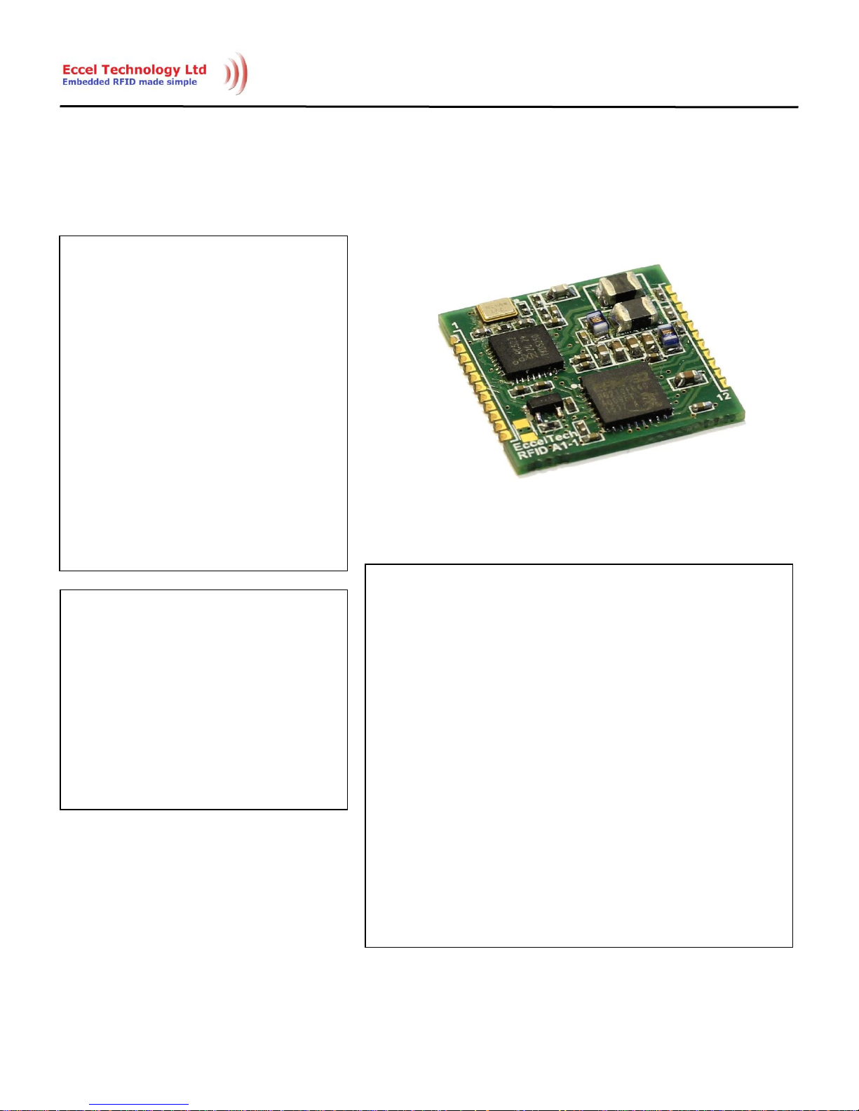
1.1 Device Overview
Features
Low cost RFID Reader with Mifare
Classic, Ultralight and NTAG2 support
Command interface via I2C and SPI
I2C speed up to 400kHz
SPI speed up to 500kHz
Compact form factor
Castellated SMT pads for easy and
reliable PCB mounting
High transponder read and write
speed
Low power design
Single operating voltage: 2.5V to 3.6V
-25°C to 85°C operating range
AES-128 encryption engine
RoHS compliant
Applications
Access control
Monitoring goods
Approval and monitoring
consumables
Pre-payment systems
Managing resources
Connection-less data storage
systems
Description
The RFID A1 module is the first in an evolving family of 13.56MHz
sub assemblies from Eccel Technology Ltd (IB Technology). The
product is designed with embedded applications in mind. This
product is an ideal design choice if the user wishes to add RFID
capability to their design quickly and without requiring extensive
RFID and embedded software expertise and time. An on board
low power ARM microcontroller handles the RFID configuration
setup and provides the user with a powerful yet simple
command interface to facilitate fast and easy read/write access
to the memory and features of the various transponders
supported by this module.
The module simply requires a single power and GND connection
from the user PCB, along with two connections to an antenna.
Eccel Technology Ltd (IB Technology) provide a range of suitable
antennas designed for use with this module.
Page 5

5
1.2 Pinout
Table 1.1
Pi n Number Sym bol Type Descri ption
1 GND Ground
2 nRESET
Digital input with
pull-up
Reset input signal (active low). This pin requires no external pull-up / down resitor
unless the module is used in noisy environments, in which case connection of an
external pull-up resistor combined with HF filter is recommended.
3 nBUSY
Digital push-pull
output
Busy signal output indicating the device is working and the user should wait with
any communication (active low) except status reading.
4 nPWRDN
Digital input with
no pull resistors
Power Down Request input signal (active low). This pin has no pull-up/down
resistor and should NOT be left floating. For power optimization it is
recommended that the user drives this pin with a push-pull GPIO or similar.
5 I2C SDA
Digital input-
outut with no pull
resistors
Data input / output for the I2C Interface Bus. This pin has no pull-up / down
resistor and should not be left floating. When using I2C communication external
pull-up resistor is required matching the I2C bus requirements.
6 I2C SCL
Digital input with
no pull resistors
Clock input for the I2C Interface Bus. This pin has no pull-up/down resistor and
should not be left floating. External pull-up resistor is required matching the I2C
bus requirements.
7 SPI MISO
Digital push-pull
output
Master In Slave Out output for the Serial Peripheral Interface Bus.
8 SPI MOSI
Digital input with
no pull resistors
Master Out Slave In input for for the Serial Peripheral Interface Bus.
9 SPI CS
Digital input with
no pull resistors
Chip Select input for the Serial Peripheral Interface Bus. This pin has no pull-up /
down resistor and should not be left floating.
10 SPI CLK
Digital input with
no pull resistors
Clock input for the Serial Peripheral Interface Bus. This pin has no pull-up / down
resistor and should not be left floating.
11 GND Ground
12 GND Ground
13 I2C AD2
Digital input with
no pull resistors
Digital input for configuring the I2C Address bit 2. Value is sampled after the reset
or power up. This pin has no pull-up / down resistor and should not be left floating.
14 I2C AD1
Digital input with
no pull resistors
Digital input for configuring the I2C Address bit 1. Value is sampled after the reset
or power up. This pin has no pull-up / down resistor and should not be left floating.
15 I2C AD0
Digital input with
no pull resistors
Digital input for configuring the I2C Address bit 0. Value is sampled after the reset
or power up. This pin has no pull-up / down resistor and should not be left floating.
16 NOT USED - -
17 NOT USED - -
18 V
DD
Power supply pin
Power Supply pin. Low ESR capacitor with capacitance 10uF or higher should be
connected close to this pin.
19 GND Ground
20 ANT2 Analog output Antenna output.
21 ANT1 Analog output Antenna output.
22 GND Ground
Page 6

6
1.3 Application
The RFID A1 module is specifically designed for embedded applications, where a fast or low pin count connection to
a host microcontroller is required. Fastest data exchange speed can be obtained by using the Serial Peripheral
Interface Bus. The lowest pin count connection can be achieved by using the I2C Bus. For the module to be a fully
functional RFID reader/writer it only requires connection to a power supply and antenna. Eccel Technology Ltd
manufactures a wide range of such antennas designed to give optimal performance with this module. Please contact
us for further details of our range of antennas.
Page 7
7
2 Electrical Characteristics
2.1 Test Conditions
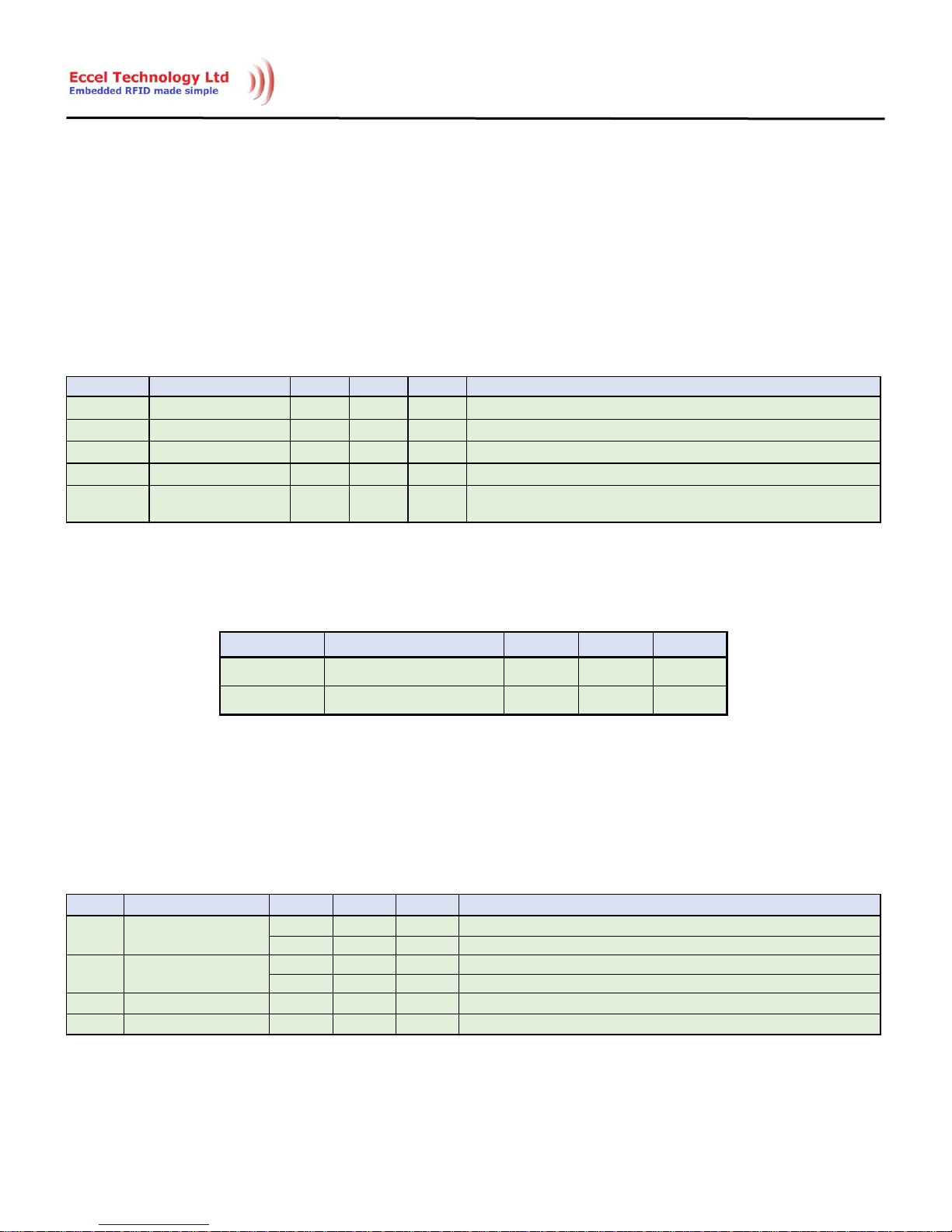
Typical device parameters have been measured at ambient temperature 22°C ±3°C and a power supply of 3.3V ±5%.
2.2 Absolute Maximum Ratings
Table 2.1
2.3 Operating Conditions
Table 2.2
2.4 Current Consumption
Table 2.3
Symbol Par amete r Min Max Uni t Note s
T
S
Storage Temperature -40 150 °C Tested for 10'000 hours at 150°C.
V
DDMAX
Supply Voltage 0 3.8 V
V
IOMAX
Input Pin Voltage -0.3 VDD + 0.3 V
I
IOMAX
Output Pin Current 0 6 mA
I
ANT
ANT1 and ANT2 Current 0 100 mA
Maximum continuous current. This depends upon the impedance of the
circuit between ANT1 and ANT2 at 13.56MHz.
Symbol Par ameter Min Ma x Unit
T
O
Ambient Temperature -25 85 °C
V
DD
Supply Voltage 2.5 3.6 V
Symbol Parameter Typ Max Unit Comment
0.9 1.1 µA T = 25°C, Vdd = 3.3V.
1.8 µA Full range of temperature and power supply voltage.
20 40 nA T = 25°C, Vdd = 3.3V.
400 nA Full range of temperature and power supply voltage.
I
TX
Power Up Current 14 24 mA T = 25°C, Vdd = 3.3V, 50Ω antenna connected between ANT1 and ANT2.
I
TXMAX
Maximum Current 120 mA Maximum current consumed by the module in the worst conditions.
Iddle Current
I
IDDLE
I
PWRDN
Power Down State
Current
Page 8

8
Current measurement was taken place with all digital input pins connected to Vdd. Pins number 16 and 17 was left
floating. Antenna was not connected except for the Power Up Current measurement and Maximum Current
measurement.
2.5 GPIO
Table 2.4
2.6 Antenna Output
Table 2.5
Symbol Para m e ter Min Typ Max Unit Note s
V
IOIL
Input Low Voltage 0.3V
DD
V
V
IOIH
Input High Voltage 0.7V
DD
V
I
IOMAX
Output Pin Current ± 6 mA
I
IOLEAK
Input Leakage Current ± 0.1 ± 40 nA High impedance IO connected to VDD or GND.
R
IOESD
Internal ESD Series
Resistor
200 Ω
V
IOHYST
IO Pin Histeresis 0.1V
DD
V
Symbol Pa r a meter Min Ty p M a x Unit N ote s
f
ANT
Antenna Signal
Frequency
13.56 MHz ±30 ppm (-20°C - 70°C).
f
ANTAG
Antenna Signal
Frequency Aging
0 3 ppm At 25°C.
V
ANTH
Antenna High Level
Output Voltage
VDD - 0.64 V VDD = 2.5V, I
ANT
= 80mA.
V
ANTL
Antenna Low Level
Output Voltage
0.64 V VDD = 2.5V, I
ANT
= 80mA.
I
ANT
ANT1 and ANT2 Current 0 60 100 mA
Maximum continuous current. This depends upon the impedance of
the circuit between ANT1 and ANT2 at 13.56MHz.
Page 9
9
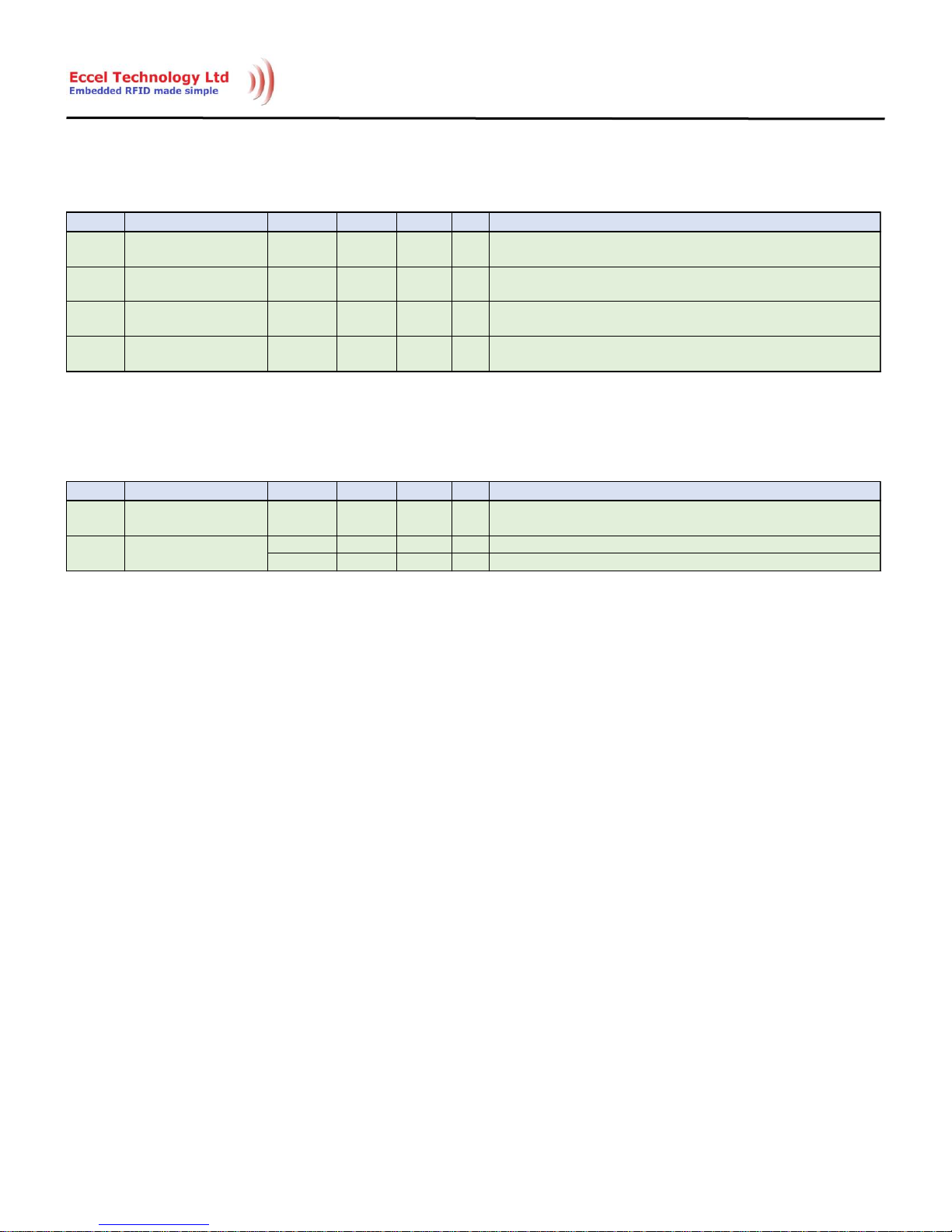
2.7 Communication Buses
Table 2.6
2.8 Flash
Table 2.7
Symbol Parameter M in Typ Max Unit Notes
f
I2CMAX
I2C Maximum Clock
Frequency
400 kHz
f
SPIMAX
SPI Maximum Clock
Frequency
500 kHz
T
CSCLK
SPI CS To CLK Time Delay 2 µs
Minimum time delay between falling edge of Chip Select and first clock
edge.
T
CSHMIN
SPI CS high Minimum Time 50 µs Minimum time when CS is in HIGH state between SPI transmissions.
Symbol Parame ter Min Typ Max Unit Notes
C
FE
Flash Erase Cycles Before
Failure
20000 cycles
10 years For ambient temperature < 85°C
20 years For ambient temperature < 70°C
T
FDR
Flash Data Retention Time
Page 10

10
3 System
3.1 Overview
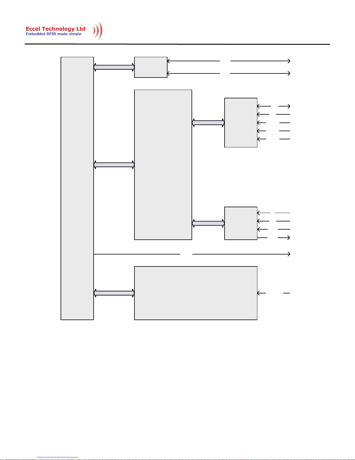
The general overview of system components is shown in Figure 3.1. The system internally consists of four main parts:
CORE – the main processing part of the microcontroller firmware responsible for managing all system tasks,
parsing and the execution of commands received from the user’s master controller.
RFID – dedicated RFID IC together with its firmware drivers responsible for communication with the RFID tag.
COMMUNICATION SYSTEM – microcontroller’s peripherals (I2C and SPI) and its firmware drivers providing
communication functionality to the user.
POWER MANAGER – a subsystem responsible for managing power states and clocks in the module to
minimise power consumption during operation.
Page 11
11
CORE
I2C
SPI
RFID
ANT1
ANT2
COMMUNICATION
SYSTEM
SDA
SCL
CS
CLK
MOSI
MISO
nBUSY
POWER MANAGER
nPWRDN
ADDR0
ADDR1
ADDR2
Figure 3.1
Page 12

12
3.2 Modules
3.2.1 Core
The core of the system shown above in figure 3.1, is the part of the modules’ hardware and firmware responsible for
managing tasks, prioritizing them and allocating resources to other components of the system. When the user sends
a command, the core is the part of the system which ensures that the command is executed properly, that the
outcome is saved and that a response is sent back to the user’s master controller.
3.2.2 RFID
The RFID component is the part of the hardware and module firmware responsible for the complete communication
interaction with the transponder via RF. In the RFID A1 module this part currently provides communication
capabilities with Mifare Classic, Ultralight and NTAG2 transponder types. The key features of this RFID section are
both fastest speed of transmission and system responsiveness, and optimal low power consumption.
3.2.3 Communication System
The Communication System component of the RFID A1 module is responsible for the entire communication with the
user master controller, together with parsing commands for subsequent execution by the module core. Two
communication interfaces are available: SPI and I2C. Both have equivalent access to the Communication System. It is
possible to communicate with the module using all two interfaces at the same time, but it is strongly recommended
to select and use only one at a time.
Communication peripherals are always active unless the nPWRDN signal is asserted. Doing so will put the module
into Deep Sleep Mode and turn off entire Communication System.
3.2.4 Power Manager
The Power Manager is the part of the firmware, together with hardware support, that manages the power states of
the system and tries to minimize power consumption as much as possible. The user has the option to put the module
into Power Down Mode by pulling low the nPWRDN pin.
When the system enters Power Down Mode, all clocks and submodules are disabled and no response to user
communication commands will occur until the system is re-enabled by the nPWDN being taken high by the user’s
system.
Page 13

13
3.3 Memory Map
The device memory layout is shown below in Table 3.1.
In the RFID A1 module there are 728 bytes of user accessible memory. Each byte of the memory has a defined
factory default value and these values can be recovered by using the ‘Reset to Factory Defaults’ command. The first
288 bytes are volatile memory which also have a default reset state that is the same as the factory default value. The
other memory is buffered non-volatile memory and can be modified and stored using ‘Unlock’ and ‘Lock’ commands.
The RFID A1 module is automatically returned to factory default state if after power up there is no valid
configuration stored in non-volatile memory. The first 288 bytes of this user accessible memory are not stored in
non-volatile memory and are always reset to factory defaults after a power-up sequence or after exit from the Power
Down Mode.
Reading and writing to the registers can be done via one of two interfaces available on the module – I2C or SPI. The
rest of the memory is accessible only when the module is unlocked. The default state of the module after power up is
locked.
Page 14

14
Table 3.1
Addr ess [DEC ] Addr ess [HEX] Si ze [by tes] D e script i on Ac c e ss
Loc ked a n d Stor ed i n non-
vol a til e m em ory
0 0x0000 1 Result Read Only No
1 0x0001 1 Command R / W No
2 0x0002 18 Command Parameters R / W No
20 0x0014 10 Tag UID Read Only No
30 0x001E 1 Tag Type Read Only No
31 0x001F 1 Tag UID Size Read Only No
32 0x0020 256 Data Buffer R / W No
288 0x0120 8 Password R / W when unlocked Yes
296 0x0128 16 AES Initialization Vector 0 R / W when unlocked Yes
312 0x0138 16 AES Initialization Vector 1 R / W when unlocked Yes
328 0x0148 16 AES Key 0 R / W when unlocked Yes
344 0x0158 16 AES Key 1 R / W when unlocked Yes
360 0x0168 6 Authentication Key / Password 0 R / W when unlocked Yes
366 0x016E 6 Authentication Key / Password 1 R / W when unlocked Yes
372 0x0174 6 Authentication Key / Password 2 R / W when unlocked Yes
378 0x017A 6 Authentication Key / Password 3 R / W when unlocked Yes
384 0x0180 6 Authentication Key / Password 4 R / W when unlocked Yes
390 0x0186 6 Authentication Key / Password 5 R / W when unlocked Yes
396 0x018C 6 Authentication Key / Password 6 R / W when unlocked Yes
402 0x0192 6 Authentication Key / Password 7 R / W when unlocked Yes
408 0x0198 6 Authentication Key / Password 8 R / W when unlocked Yes
414 0x019E 6 Authentication Key / Password 9 R / W when unlocked Yes
420 0x01A4 6 Authentication Key / Password 10 R / W when unlocked Yes
426 0x01AA 6 Authentication Key / Password 11 R / W when unlocked Yes
432 0x01B0 6 Authentication Key / Password 12 R / W when unlocked Yes
438 0x01B6 6 Authentication Key / Password 13 R / W when unlocked Yes
444 0x01BC 6 Authentication Key / Password 14 R / W when unlocked Yes
450 0x01C2 6 Authentication Key / Password 15 R / W when unlocked Yes
456 0x01C8 6 Authentication Key / Password 16 R / W when unlocked Yes
462 0x01CE 6 Authentication Key / Password 17 R / W when unlocked Yes
468 0x01D4 6 Authentication Key / Password 18 R / W when unlocked Yes
474 0x01DA 6 Authentication Key / Password 19 R / W when unlocked Yes
480 0x01E0 6 Authentication Key / Password 20 R / W when unlocked Yes
486 0x01E6 6 Authentication Key / Password 21 R / W when unlocked Yes
492 0x01EC 6 Authentication Key / Password 22 R / W when unlocked Yes
498 0x01F2 6 Authentication Key / Password 23 R / W when unlocked Yes
504 0x01F8 6 Authentication Key / Password 24 R / W when unlocked Yes
510 0x01FE 6 Authentication Key / Password 25 R / W when unlocked Yes
516 0x0204 6 Authentication Key / Password 26 R / W when unlocked Yes
522 0x020A 6 Authentication Key / Password 27 R / W when unlocked Yes
528 0x0210 6 Authentication Key / Password 28 R / W when unlocked Yes
534 0x0216 6 Authentication Key / Password 29 R / W when unlocked Yes
540 0x021C 6 Authentication Key / Password 30 R / W when unlocked Yes
546 0x0222 6 Authentication Key / Password 31 R / W when unlocked Yes
552 0x0228 6 Authentication Key / Password 32 R / W when unlocked Yes
558 0x022E 6 Authentication Key / Password 33 R / W when unlocked Yes
564 0x0234 6 Authentication Key / Password 34 R / W when unlocked Yes
570 0x023A 6 Authentication Key / Password 35 R / W when unlocked Yes
576 0x0240 6 Authentication Key / Password 36 R / W when unlocked Yes
582 0x0246 6 Authentication Key / Password 37 R / W when unlocked Yes
588 0x024C 6 Authentication Key / Password 38 R / W when unlocked Yes
594 0x0252 6 Authentication Key / Password 39 R / W when unlocked Yes
600 0x0258 128 User Memory R / W when unlocked Yes
Page 15

15
3.3.1 Result Register
The Result Register is 1-byte long, with located at address 0x0000, with both read and write access. Writing to this
register has no effect. The register contains the result (error code) of the last executed command. The list of all
possible results is shown in Table 3.2.
Table 3.2
Val ue T ype Descr iption
0x00 No Error
Command was executed successfully and results were
stored in the registers.
0x01 Invalid Command Value written to command register is invalid.
0x02 Invalid Command Parameter
One of the parameters taken by the command is
invalid.
0x03 Indexes Out Of Range Indexes passed as command parameters exceed limit.
0x04
Error When Writing To Non
Volatile Memory
There was an internal error during writing to the non-
volatile memory.
0x05 System Error Internal system error. Shall be considered as fatal.
0x06 Tag CRC Error
During communication with the tag a CRC was not
correct.
0x07 Tag Collision Reserved for future use.
0x08 Tag is not present There is no tag within range.
0x09 Tag Authentication Error
Authentication failed due to incorrect Autentication
Key or Password.
0x0A Tag Value Block Corrupted
At least one value block is corrupted in the tag
memory.
0x0B Module Overheated A overheat was detected.
0x0C Tag Not Supported There is a tag in the field which is not supported.
0x0D Tag Communication Error There was an error during communication with the tag.
0x0E Invalid Password
The Password used in the Unlock command string was
invalid.
0x0F Already Locked
You are trying to lock a module that is already locked.
0xFF Module Busy
Your command was ignored because the module is
busy. Retry later.
Result Reg ister Va lues
Page 16
16
3.3.2 Command Register
The Command Register is 1-byte, located at address 0x0001, with both read and write access. Writing to this register
is recognized by the module as a command execution request. Depending upon the command (value written to the
register) the Command Parameters Register is parsed to extract arguments for the command. Whilst commands are
executing, the Result Register value is set to 0xFF and the nBUSY line is driven low. When command execution is
complete the memory is updated and the nBUSY line returns to the high state indicating that the module is ready to
receive another command.
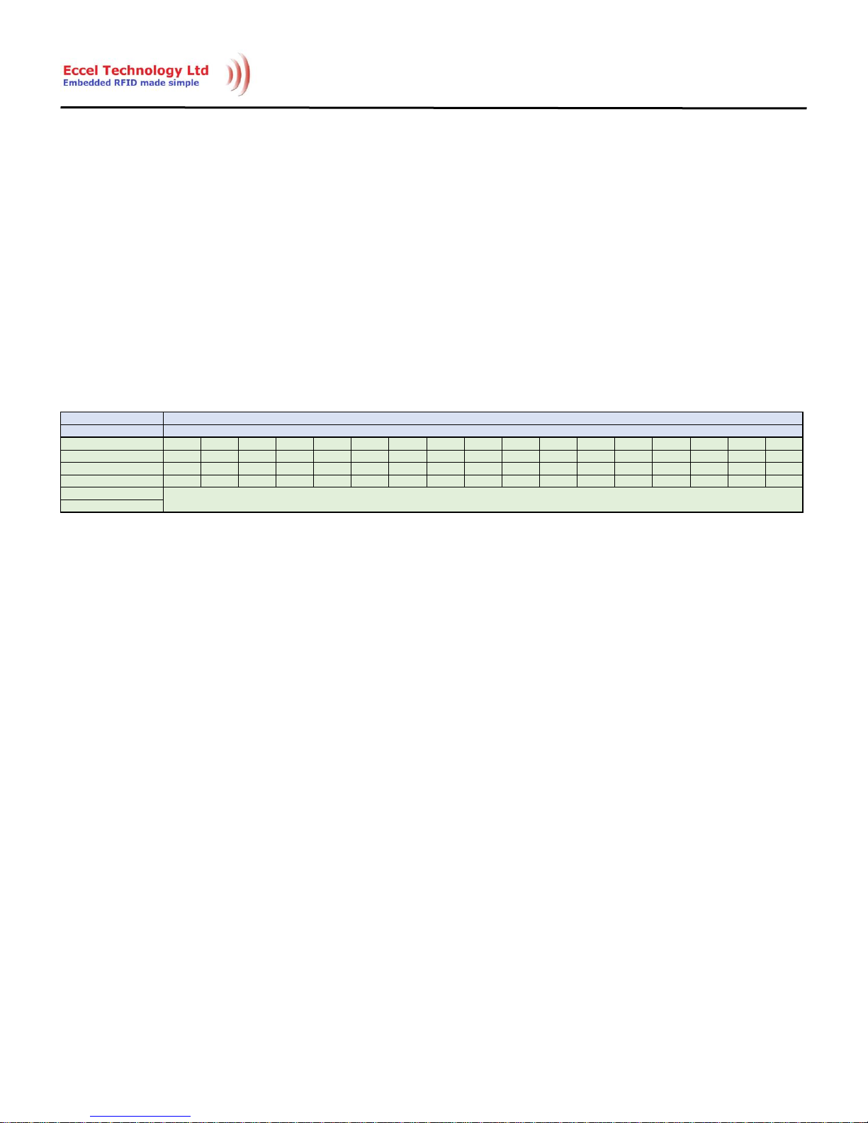
3.3.3 Command Parameters Register
Table 3.3
The Command Parameters Register is 18-bytes long, located at addresses from 0x0002 to 0x0013, with both read
and write access. This is the place from where the system parses the arguments necessary to perform requested
operation when a command is executed. Depending upon the command, this register is parsed and interpreted in
different ways. The details of interpretation of the data stored in this register can be found in chapter 4.2. The
module never changes the values inside this register except after power-up or exit from Deep Sleep Mode.
Re giste r Na me
Re giste r Add ress
By te Offs et
0x00 0x01 0x02 0x03 0x04 0x05 0x06 0x07 0x08 0x09 0x0A 0x0B 0x0C 0x0D 0 x0E 0x0F 0 x10
By te Pos iti on
0 1 2 3 4 5 6 7 8 9 10 11 12 13 14 15 16
Ac cess
R/W R/W R/W R/W R/W R/W R/W R/W R/W R/W R/W R/W R/W R/W R/W R/W R/W
Fa ct ory Def aul t V al ue
0x00 0x00 0x00 0x00 0x00 0x00 0x00 0x00 0x00 0x00 0x00 0x00 0x00 0x00 0x00 0x00 0x00
Re ad Funct ion
Wr ite F uncti on
Parameters taken when executing commands. Each command has various number and order of parameters.
Command Parameters
0x0002
Page 17
17
3.3.4 Tag UID Register
Table 3.4
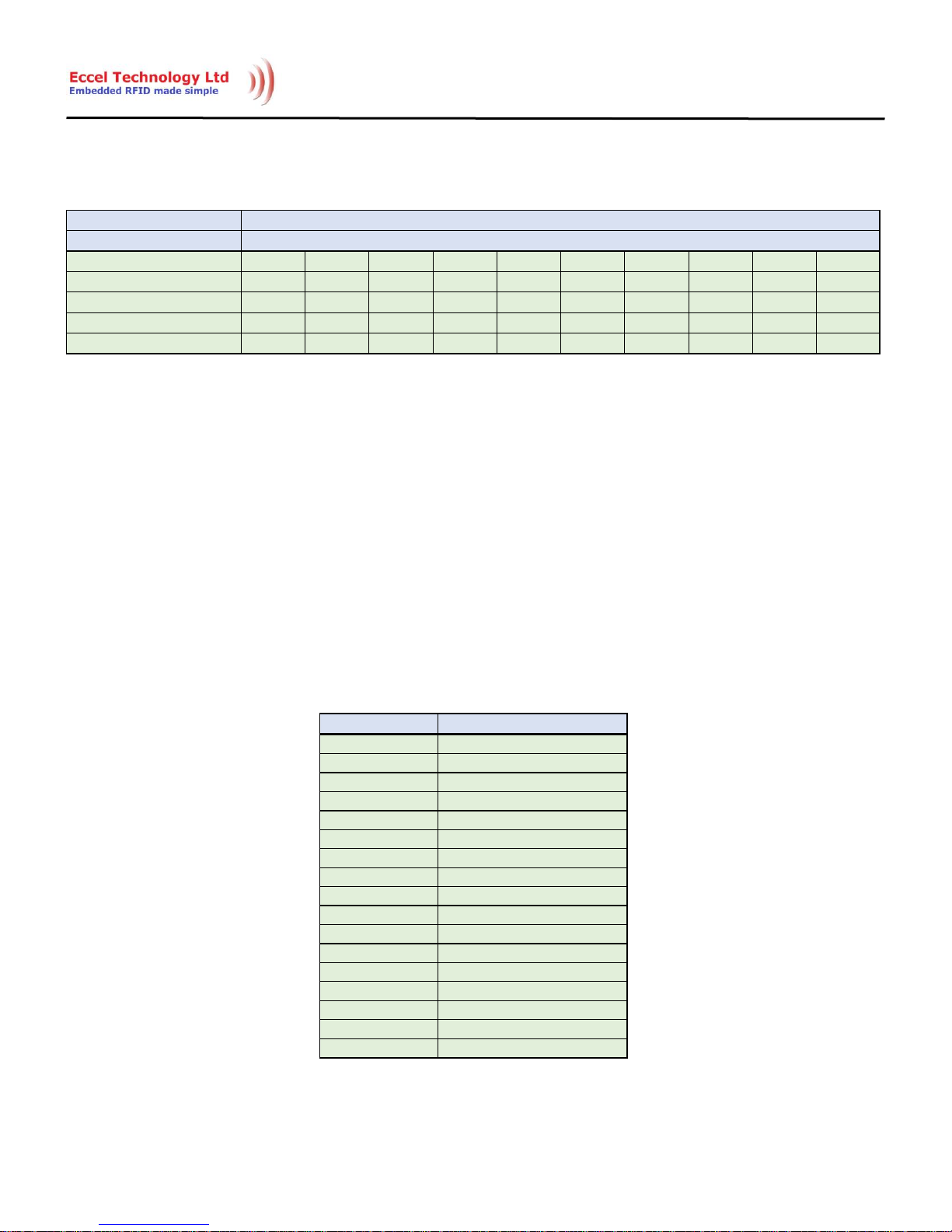
Tag UID Register is 10-bytes long, located at addresses from 0x0014 to 0x001D, with read only access. In most cases
the tag UIDs are 4 bytes, 7 bytes or 10 bytes long, thus this register can cover the longest UID but not necessarily all
bytes available in the register will be used. Bytes within the register are ordered from the least significant byte to the
most significant byte. This register is updated whenever Get UID and Type commands are used. The Tag UID Size
Register contains information detailing how many bytes of the ten available represent the tag UID.
3.3.5 Tag Type Register
The Tag Type Register is 1-byte long located at address 0x001E, with read only access. This register contains
information about the type of tag which was last seen in the field. Possible tag types are shown in Table 3.5.
Table 3.5
Re gister N ame
Re gister Addre ss
By t e Offset
0x00 0x01 0x02 0x03 0x04 0x05 0x06 0x07 0x08 0x09
By t e Posit ion
0 1 2 3 4 5 6 7 8 9
Access
R R R R R R R R R R
Fac t ory Default Value
0x00 0x00 0x00 0x00 0x00 0x00 0x00 0x00 0x00 0x00
Re ad Func t ion
UID[0] UID[1] UID[2] UID[3] UID[4] UID[5] UID[6] UID[7] UID[8] UID[9]
Tag UID
0x0014
Retur ned val ue Ta g ty pe
0x00 No Tag
0x01 Incomplete Type
0x02 Ultralight
0x03 Ultralight EV1 80B
0x04 Ultralight EV1 164B
0x05 Classic Mini
0x06 Classic 1K
0x07 Classic 4K
0x08 NTAG203F
0x09 NTAG210
0x0A NTAG212
0x0B NTAG213F
0x0C NTAG216F
0x0D NTAG213
0x0E NTAG215
0x0F NTAG216
0x10 Unknown
Page 18
18
3.3.6 Tag UID Size Register
The Tag UID Size Register is 1-byte long, located at address 0x001F, with read only access. It contains the information
of what the UID size in bytes was of the last tag in the field.
3.3.7 Data Buffer
The Data Buffer is a 256-byte long, located at address 0x0020 to 0x011F, with both read and write access. This buffer
is used for data transfers between the tag and the user of the module.
3.3.8 Password Register
Table 3.6
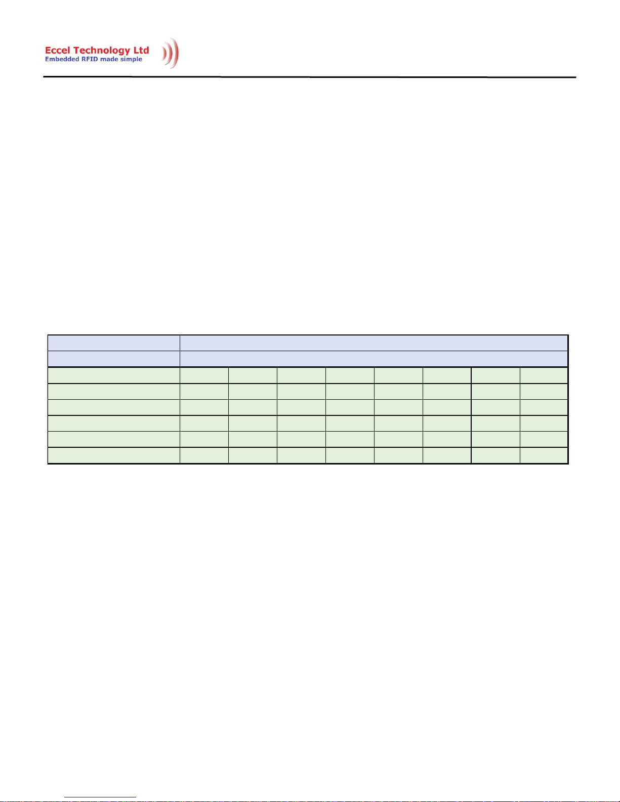
The Password Register is 8-bytes long, located at address 0x0120 to 0x0127, with both read and write access but only
after first unlocking the device. This register is inaccessible when the module is locked. It contains an 8-byte long
password which must be used with the Unlock Command to unlock protected memory. This password can be
changed when the device is unlocked. The password change will only be updated and become valid after executing
the Lock command.
Reg ister Na me
Reg ister Addr ess
Byte Offset
0x00 0x01 0x02 0x03 0x04 0x05 0x06 0x07
Byte Positi on
0 1 2 3 4 5 6 7
Access
R/W R/W R/W R/W R/W R/W R/W R/W
Fa ctor y Def ault V a lue
0x00 0x00 0x00 0x00 0x00 0x00 0x00 0x00
Rea d Func ti on
PASS[0] PASS[1] PASS[2] PASS[3] PASS[4] PASS[5] PASS[6] PASS[7]
Wr ite Function PASS[0] PASS[1] PASS[2] PASS[3] PASS[4] PASS[5] PASS[6] PASS[7]
Password
0x0120
Page 19
19
3.3.9 AES Initialization Vector Register
Table 3.7
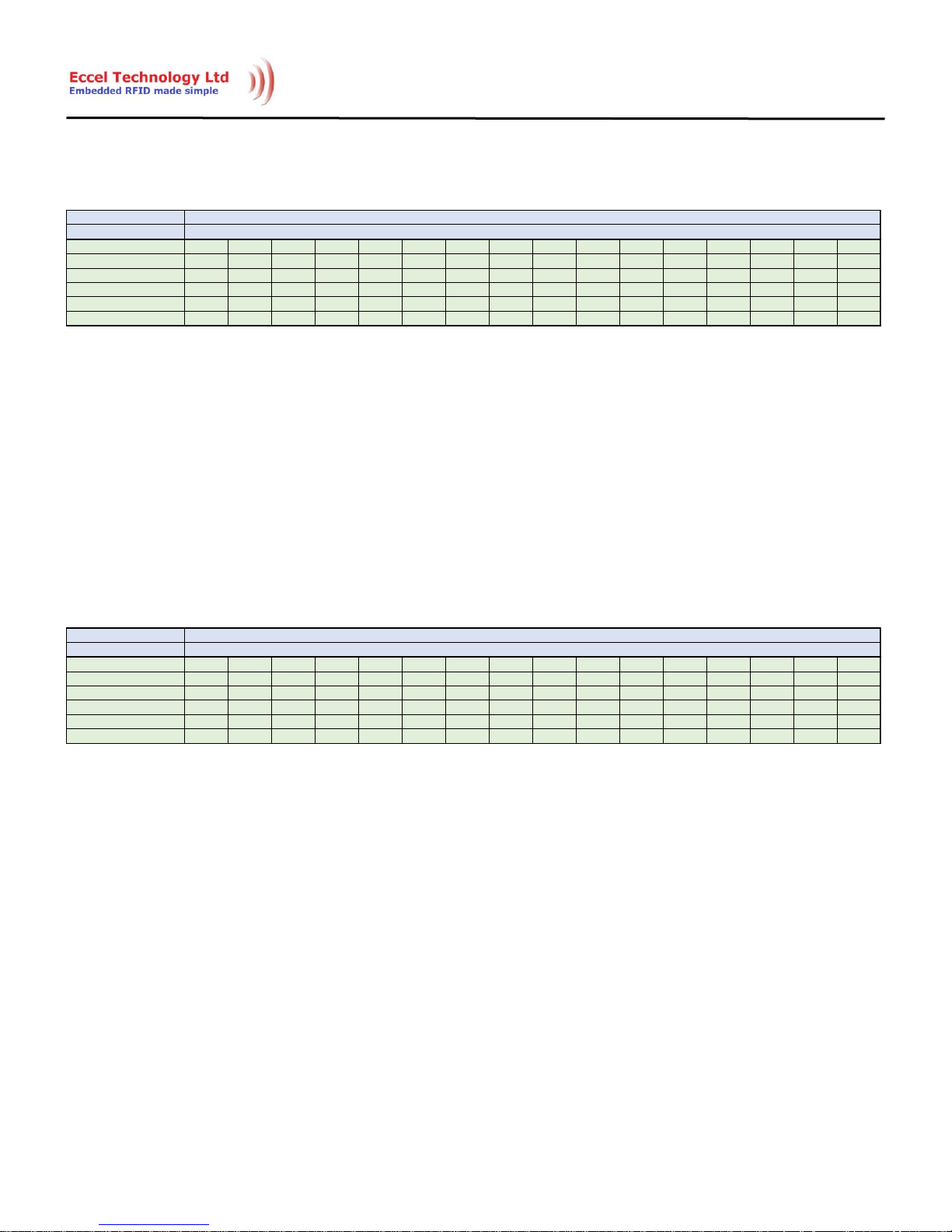
The AES Initialization Vector Registers are two 16-bytes long registers, located at address 0x0128 to 0x0147, with
both read and write access but only after first unlocking the device. These registers are inaccessible when the
module is locked. They can be used as an initialization vector for the first encrypted data block. The byte order in the
memory is from the least significant byte. Their role during data encryption and decryption is described in detail in
chapter 4.2.8 and 4.2.9.
3.3.10 AES Key Register
Table 3.8
The AES Key Registers are two 16-bytes long registers, located at address 0x0148 to 0x0167, with both read and
write access but only after first unlocking the device. These registers are inaccessible when the module is locked.
Both registers contain an AES encryption key which can be used for encryption of the Data Buffer. Their role during
encryption and decryption of the data in the buffer is described in detail in chapter 4.2.8 and 4.2.9.
Re gister Na me
Re gister Addr ess
By te Offs et
0x00 0x01 0x02 0x03 0x04 0x05 0x06 0x07 0x08 0x09 0x0A 0x0B 0x0C 0x0D 0x0E 0x0F
By te Pos iti on
0 1 2 3 4 5 6 7 8 9 10 11 12 13 14 15
Ac ces s
R/W R/W R/W R/W R/W R/W R/W R/W R/W R/W R/W R/W R/W R/W R/W R/W
Fa ctor y D efa ult V alue
0x00 0x00 0x00 0x00 0x00 0x00 0x00 0x00 0x00 0x00 0x00 0x00 0 x00 0x00 0x00 0x00
Re ad Funct ion
InVec[0] InVec[1] InVec[2] InVec[3] InVec[4] InVec[5] InVec[6] InVec[7] InVec[8] InVec[9] InVec[10] InVec[11] InVec[12] InVec[13] InVec[14] InVec[15]
Wr ite Funct i on InVec[0] InVec[1] InVec[2] InVec[3] InVec[4] InVec[5] InVec[6] InVec[7] InVec[8] InVec[9] InVec[10] InVec[11] InVec[12] InVec[13] InVec[14] InVec[15]
0x0128,0x0138
AES Initialization Vector
Re gister Na me
Re gister Addr ess
By te Offs et
0x00 0x01 0x02 0x03 0x04 0x05 0x06 0x07 0x08 0x09 0x0A 0x0B 0x0C 0x0D 0x0E 0x0F
By te Pos iti on
0 1 2 3 4 5 6 7 8 9 10 11 12 13 14 15
Ac ces s
R/W R/W R/W R/W R/W R/W R/W R/W R/W R/W R/W R/W R/W R/W R/W R/W
Fa ctor y D efa ult V alue
0x00 0x00 0x00 0x00 0x00 0x00 0x00 0x00 0x00 0x00 0x00 0x00 0 x00 0x00 0x00 0x00
Re ad Funct ion
Key[0] Key[1] Key[2] Key[3] K ey[4] Key[5] Key[6] Key[7] K ey[8] Key[9] Key[10] Key[11] Key[12] Key[13] Key[14] Key[15]
Wr ite Funct i on Key[0] Key[1] Key[2] Key[3] Key[4] Key[5] Key[6] Key[7] Key[8] Key[9] Key[10] Key[11] Key[12] Key[13] Key[14] Key[15]
0x0148, 0x0158
AES Key
Page 20
20
3.3.11 Authentication Key / Password Register
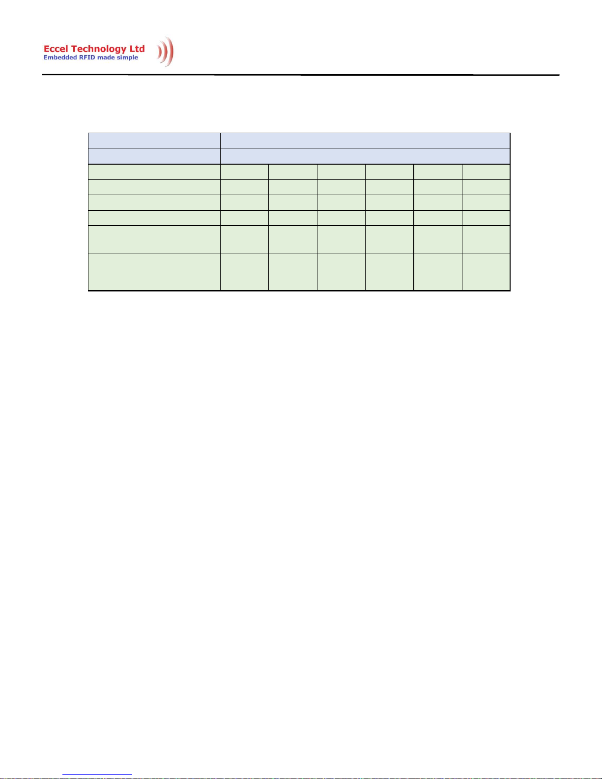
Table 3.9
The Authentication Key and Password Registers are forty 6-bytes long registers, located at address 0x0168 to 0x0257,
with both read and write access but only after first unlocking the device. These registers are inaccessible when the
module is locked. When working with Mifare Classic tags these registers contain the password keys used for block
authentication in the tag. When working with Ultralight and NTAG transponders, these registers contain 4-byte
passwords. There are forty Authentication Key and Password registers numbered from 0 to 39. The number of the
key register to be used is passed as an argument in some commands.
3.3.12 User Memory
There are 128 bytes of memory available for the user as a protected memory space from address 0x0258 to 0x02D7.
This memory is inaccessible when the device is locked. This data is stored into non-volatile memory when the Lock
command is executed.
Register Name
Register Address
Byte Offs et
0x00 0x01 0x02 0x03 0x04 0x05
Byte Position
0 1 2 3 4 5
Acc ess
R/W R/W R/W R/W R/W R/W
Factory Default Value
0x00 0x00 0x00 0x00 0x00 0x00
Read Func tion
KEY[0] /
PASS[0]
KEY[1] /
PASS[1]
KEY[2] /
PASS[2]
KEY[3] /
PASS[3]
KEY[4] KEY[5]
Write Funct ion
KEY[0] /
PASS[0]
KEY[1] /
PASS[1]
KEY[2] /
PASS[2]
KEY[3] /
PASS[3]
KEY[4] KEY[5]
0x0168, 0x016E … 0x0252
Authentication Key / Password
Page 21

21
4 Functional Description
4.1 Overview
The RFID A1 module is designed to provide a simple interface to communicate and manage RFID tags from the
Mifare Classic, Ultralight and NTAG2 families. The interface is provided via SPI and I2C busses. From the user
perspective, the module is a memory region where he can read from and write to. Depending upon the memory
address, the role of registers located in the memory differ as per the Memory Map description given in Chapter 3.3.
By writing to and reading from these registers, the user can achieve the desired result.
4.2 Commands
The RFID A1 Module has a special register, the Command Register. Writing to this register is interpreted as a
command execution request from the user. The command type corresponds to the value written into the register.
Execution of a command starts when the communication is finished. Depending upon the bus used, definition of the
communication endpoint varies. When using the I2C bus, communication is finished when a STOP condition is sent.
In case of the SPI bus, communication is finished on the rising edge of the CS signal.
The nBUSY line goes from the high state to the low state and indicates that the module is busy (it parses data stored
in the registers and executes commands, if any command was sent). A more detailed description of the signal
behavior is given in chapter 5.1.
The full RFID A1 command list is shown below in Table 4.1.
Page 22

22
Table 4.1
Val ue Com mand Ty pe
Ar guments T a ke n M emor y Modi f ied
0x00 No action
- -
0x01 Get UID and Type
-
Result Register, Tag Type, Tag UID,
Tag UID Size
0x02 Read Block
Block Address, Read Length, Authentication Key
Number, Authentication Key, Buffer Offset
Result Register, Data Buffer
0x03 Write Block
Block Address, WriteLength, Authentication Key
Number, Authentication Key, Buffer Offset
Result Register
0x04 Read Data Block
Block Address, Read Length, Authentication Key
Number, Authentication Key, Buffer Offset
Result Register, Data Buffer
0x05 Write Data Block
Block Address, Read Length, Authentication Key
Number, Authentication Key, Buffer Offset
Result Register
0x06 Read Page
Page Address, Read Length, Buffer Offset Result Register, Data Buffer
0x07 Write Page
Page Address, Read Length, Buffer Offset Result Register
0x08 Encrypt Data
Encryption Key Number, Initialization Vector Number,
Buffer Offset, Data Length
Result Register, Data Buffer
0x09 Decrypt Data
Encryption Key Number, Initialization Vector Number,
Buffer Offset, Data Length
Result Register, Data Buffer
0x0A Read Value
Block Address, Authentication Key Number,
Authentication Key, Buffer Offset
Result Register, Data Buffer
0x0B Write Value
Block Address, Authentication Key Number,
Authentication Key, 32-bit signed Value, Stored Block
Address
Result Register
0x0C Increment Value
Block Address, Authentication Key Number,
Authentication Key, 32-bit signed Delta Value
Result Register
0x0D Decrement Value
Block Address, Authentication Key Number,
Authentication Key, 32-bit signed Delta Value
Result Register
0x0E Restore Value
Block Address, Authentication Key Number,
Authentication Key
Result Register
0x0F Transfer Value
Block Address, Authentication Key Number,
Authentication Key
Result Register
0x10 Recover Value
Block Address, Buffer Offset, Authentication Key
Number, Authentication Key
Result Register
0x11 Get Version
- Result Register, Data Buffer
0x12 Read Signature
- Result Register, Data Buffer
0x13 Configure UID
Authentication Key Number, Authentication Key, UID
Type
Result Register
0x14 Read Counter
Counter Number, Buffer Offset Result Register, Data Buffer
0x15 Increment Counter
Counter Number, 24-bit signed Increment Value Result Register
0x16 Check Tearing Event
Counter Number, Buffer Offset Result Register, Data Buffer
0x17 Password Authentication
Buffer Offset, Password Number, Password Result Register, Data Buffer
0x18 Halt
- Result Register
0x19 Calculate CRC
Memory Address, Data Legth, Buffer Offset Data Buffer
0x1A Copy Data
Destination Address, Source Address, Data Length All
0x1B Unlock
Password Result Register
0x1C Lock
- Result Register, Non-volatile memory
0x1D Get Module Version
- Data Buffer
Page 23

23
Depending upon the command, different arguments are taken as parameters and various registers are modified.
After each command execution, the Result Register is updated.
4.2.1 Get UID and Type (0x01)
The ‘Get UID and Type’ command takes no arguments. After receiving this command, the RFID A1 Module checks for
any tag presence in the field. If there is no tag in the field, it returns ‘No Tag’ value in the ‘Tag Type Register’. If
there is a tag in the field, it reads its UID and type and writes it to Tag UID and Tag Type registers. The ‘UID Size
Register’ together with the ‘Result Register’ are updated also. This command must always be executed first before
any other command to turn on and initialize the tag. Additionally, this command must be executed after any error
when doing any operations on a tag to reset the tag and to enable it to be able to respond to further command
requests.
Page 24
24
4.2.2 Read Block (0x02)
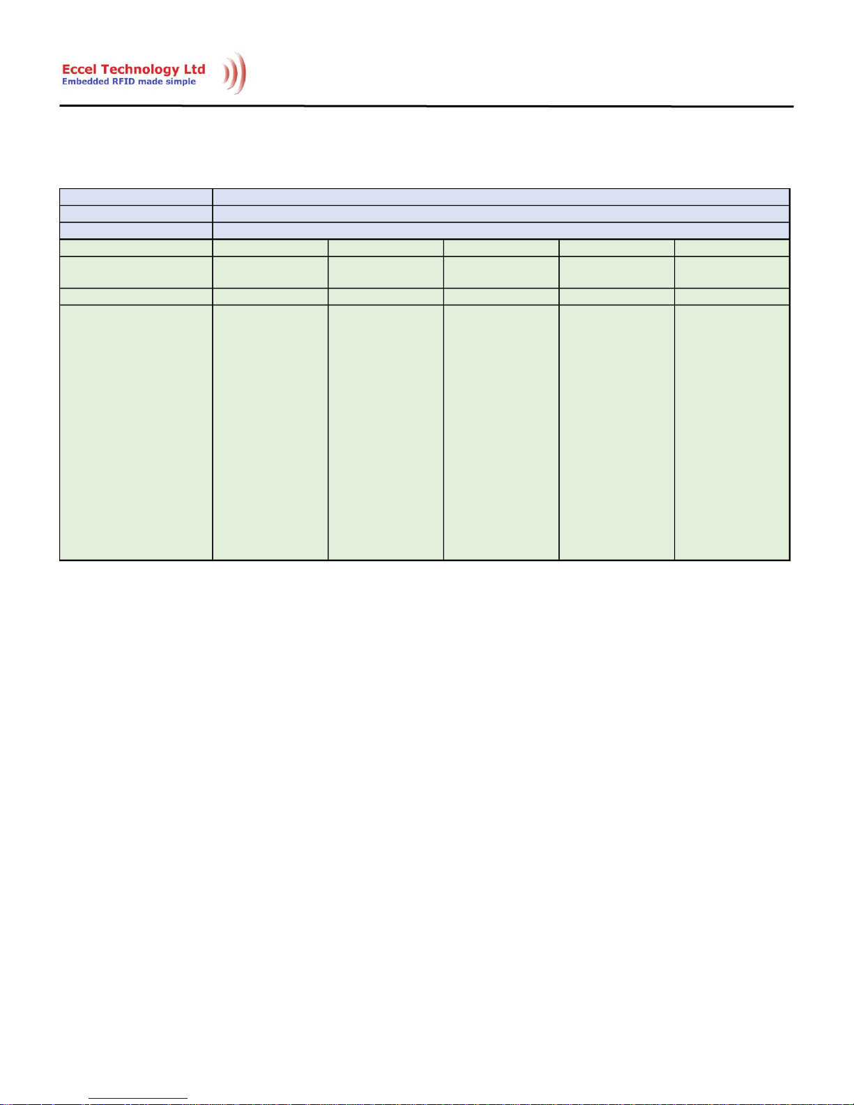
Table 4.2
The ‘Read Block’ command takes as arguments the first block address to read (Block Address), the number of blocks
to read (Read Length), the byte offset in the data buffer (Data Buffer Offset), the Authentication Key Number and
(optionally) the Authentication Key. If the Authentication Key is set-up, the command first tries to authenticate the
sector which contains the first buffer. If authentication fails, the ‘Result Register’ is updated with the appropriate
error value and command execution finishes. After a successful authentication, the first block is read and stored in
the data buffer. The command continues to read following blocks if the Read Length is higher than 1. If the next
blocks fall into another tag memory sector this sector is authenticated using the same key. If everything goes well all
block bytes are copied to the Data Buffer starting from Data Buffer Offset and the Result Register is updated with the
‘No Error’ value. If the RFID Module is unable to read the block, an error value is stored in the Result Register.
Com m a nd Num ber
Com m a nd Na me
Va li d Tag T y pes
Ar gum e nt Offse t [ bytes]
0x00 0x01 0x02 0x03 0x04
Ar gum e nt Na m e Block Address Read Length Data Buffer Offset
Authentication Key
Number
Authentication Key
Ar gum e nt Si ze [by tes]
0x01 0x01 0x01 0x01 0x06
Ar gum e nt D e scr i pti on
Address of the first
block in the memory
that is to be read.
Number of blocks to
read. Value has to be
larger than 0.
Buffer offset in bytes of
where the data from
the tag is to be stored.
The total read size and
the offset must not
exceed the data buffer
length (number of
bytes).
The 6 least significant
bits define the
Authentication Key
Number from 0 to 39
that is to be used to
decrypt the data read.
If the most significant
bit (bit 7) is set, then
the key will be used as
key B. If bit 7 is zero it
will be used as key A. If
bit 6 is set, then the
key will be taken from
the following argument
list (next 6 bytes).
Optional parameter
used when bit 6 in
Authentication Key
Number argument is
set. This Key will be
used as Key B if bit 7 in
Authentication Key
Number is set or as Key
A if bit 7 is not set. The
byte order is the least
significant byte first.
0x02
Read Block
Mifare Classic
Page 25
25
4.2.3 Write Block (0x03)
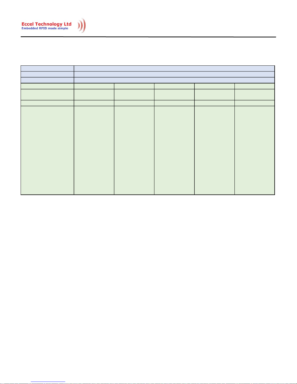
Table 4.3
The Write Block command takes as arguments the first block address to write (Block Address), the number of blocks
to write (Write Length), the byte offset in the data buffer (Data Buffer Offset), the Authentication Key Number and
(optionally) the Authentication Key. If the Authentication Key is set-up, the command first tries to authenticate the
sector which contains the first buffer. If authentication fails, the Result Register is updated with the appropriate
error code and command execution finishes. After successful authentication, the data is transferred from the data
buffer to the first block. The command continues to write to the following blocks if the Write Length is higher than 1.
If subsequent blocks fall into another tag memory sector this sector is authenticated using the same key. If
everything goes well all block bytes are copied from the Data Buffer starting from Data Buffer Offset, and the Result
Register is updated with the ‘No Error’ code. If the RFID Module is unable to write to the blocks an appropriate error
code is stored in the Result Register.
Com m a nd Num ber
Com m a nd Na me
Va li d Tag T y pes
Ar gum e nt Offse t [ bytes]
0x00 0x01 0x02 0x03 0x04
Ar gum e nt Na m e Block Address Write Length Data Buffer Offset
Authentication Key
Number
Authentication Key
Ar gum e nt Si ze [by tes]
0x01 0x01 0x01 0x01 0x06
Ar gum e nt D e scr i pti on
Address of the first
block in the memory to
which the data is to be
written.
Number of blocks to
write. Value has to be
larger than 0.
Buffer offset in bytes
from where the data is
to be taken to write to
the tag. The total write
size and the offset
must not exceed the
data buffer length
(number of bytes).
The 6 least significant
bits define the
Authentication Key
Number from 0 to 39
that is to be used to
encrypt the data that is
to be written. If the
most significant bit (bit
7) is set, then the key
will be used as key B. If
bit 7 is zero it will be
used as key A. If bit 6 is
set, then the key will be
taken from the
following argument list
(next 6 bytes).
Optional parameter
used when bit 6 in
Authentication Key
Number argument is
set. This Key will be
used as Key B if bit 7 in
Authentication Key
Number is set or as Key
A if bit 7 is not set. The
byte order is the least
significant byte first.
Mifare Classic
0x03
Write Block
Page 26
26
4.2.4 Read Data Block (0x04)
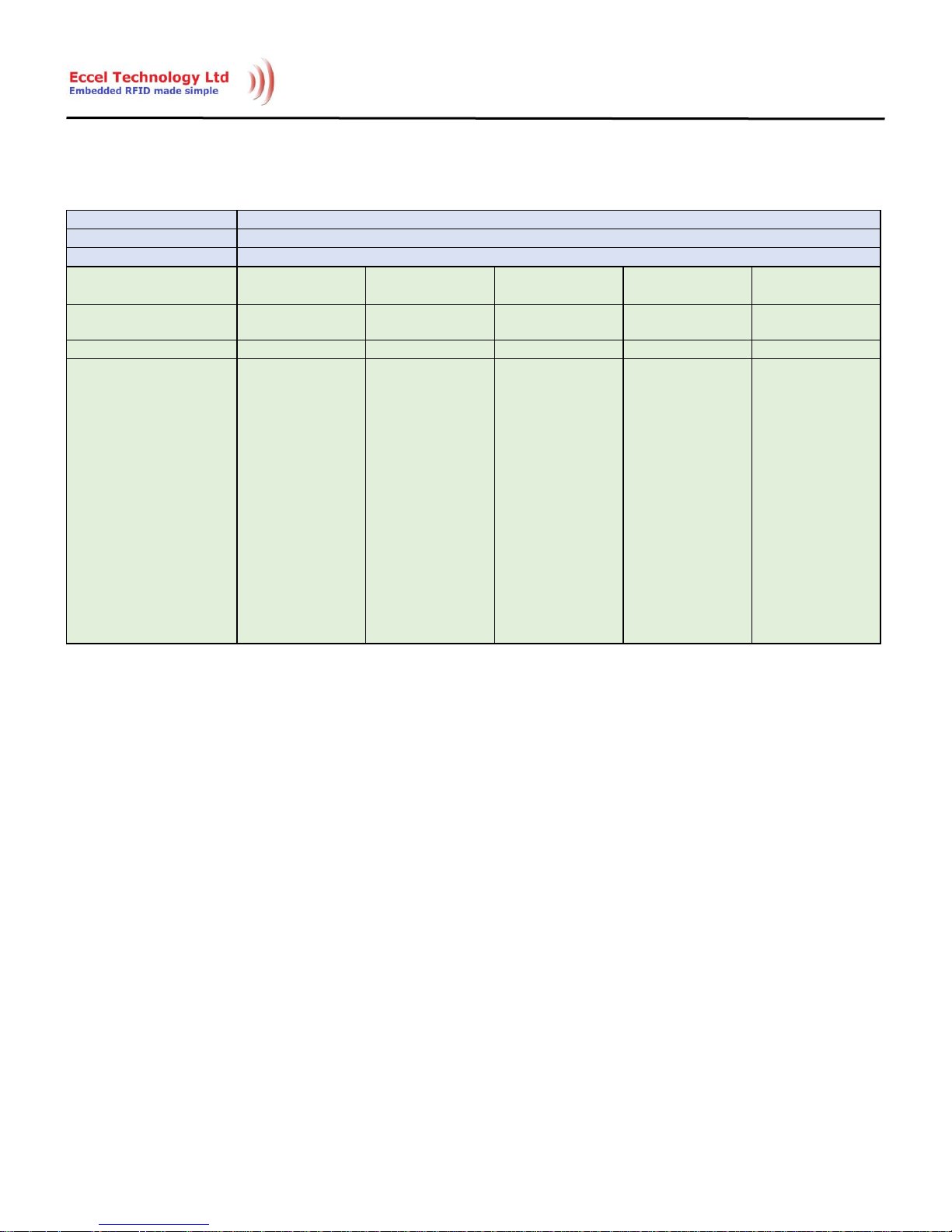
Table 4.4
The Read Data Block command takes as arguments the first block address to read (Block Address), the number of
blocks to read (Read Length), the byte offset in the data buffer (Data Buffer Offset), the Authentication Key Number
and (optionally) the Authentication Key. If the Authentication Key is set-up, the command first tries to authenticate
the sector which contains the first buffer. If authentication fails, the Result Register is updated with the ‘error’ value
and command execution finishes. After successful authentication, the first block is read and stored in the data
buffer. The command continues to read subsequent blocks if the Read Length is higher than 1. The difference
between the Read Data Block command and the Read Block Command is that the first one omits blocks with
authentication keys and lock bits. It only reads the data blocks from Mifare tags. If the subsequent blocks read fall
into another tag memory sector, this sector is authenticated using the same key. If everything goes well all block
bytes are copied to the Data Buffer starting from the Data Buffer Offset and the Result Register is updated with a ‘No
Error’ value. If the RFID Module is unable to read the block an ‘error’ value is stored in the Result Register.
Com m a nd Num ber
Com m a nd Na me
Va li d Tag T y pes
Ar gum e nt Offse t [ bytes] 0x00 0x01 0x02 0x03 0x04
Ar gum e nt Na m e Block Address Read Length Data Buffer Offset
Authentication Key
Number
Authentication Key
Ar gum e nt Si ze [by tes]
0x01 0x01 0x01 0x01 0x06
Ar gum e nt D e scr i pti on
Address of the first
block in the memory
that is to be read.
Number of blocks to
read. Value has to be
larger than 0.
Buffer offset in bytes of
where the data from
the tag is to be stored.
The total read size and
the offset must not
exceed the data buffer
length (number of
bytes).
The 6 least significant
bits define the
Authentication Key
Number from 0 to 39
that is to be used to
decrypt the data read.
If the most significant
bit (bit 7) is set, then
the key will be used as
key B. If bit 7 is zero it
will be used as key A. If
bit 6 is set, then the
key will be taken from
the following argument
list (next 6 bytes).
Optional parameter
used when bit 6 in
Authentication Key
Number argument is
set. This Key will be
used as Key B if bit 7 in
Authentication Key
Number is set or as Key
A if bit 7 is not set. The
byte order is the least
significant byte first.
0x04
Read Data Block
Mifare Classic
Page 27
27
4.2.5 Write Data Block (0x05)
Table 4.5
The Write Data Block command takes as arguments the first block address to write (Block Address), the number of
blocks to write (Write Length), the byte offset in the data buffer (Data Buffer Offset), the Authentication Key Number
and (optionally) the Authentication Key. If the Authentication Key is set-up, the command first tries to authenticate
the sector which contains the first buffer. If authentication fails, the Result Register is updated with an ‘error’ value
and command execution terminates. After successful authentication, the data is transferred from the data buffer to
the first block. The Command continues to write to subsequent blocks if the Write Length is higher than 1. The
difference between Write Data Block command and Write Block Command is that the first one omits blocks with
authentication keys and lock bits. It only writes to the data blocks of Mifare tags. If subsequent blocks fall into
another sector this sector is authenticated using the same key. If everything goes well all block bytes are copied
from the Data Buffer starting from the Data Buffer Offset and the Result Register is updated with a ‘No Error’ value.
If the RFID Module is unable to write to the blocks an ‘error’ value is stored in the Result Register.
Com m a nd Num ber
Com m a nd Na me
Va li d Tag T y pes
Ar gum e nt Offse t [ bytes] 0x00 0x01 0x02 0x03 0x04
Ar gum e nt Na m e Block Address Write Length Data Buffer Offset
Authentication Key
Number
Authentication Key
Ar gum e nt Si ze [by tes]
0x01 0x01 0x01 0x01 0x06
Ar gum e nt D e scr i pti on
Address of the first
block in the memory to
which the data will be
written.
Number of blocks to
write. Value has to be
larger than 0.
Buffer offset in bytes
from where the data is
to be taken to write to
the tag. The total write
size and the offset
must not exceed the
data buffer length
(number of bytes).
The 6 least significant
bits define the
Authentication Key
Number from 0 to 39
that is to be used to
encrypt the data that is
to be written. If the
most significant bit (bit
7) is set, then the key
will be used as key B. If
bit 7 is zero it will be
used as key A. If bit 6 is
set, then the key will be
taken from the
following argument list
(next 6 bytes).
Optional parameter
used when bit 6 in
Authentication Key
Number argument is
set. This Key will be
used as Key B if bit 7 in
Authentication Key
Number is set or as Key
A if bit 7 is not set. The
byte order is the least
significant byte first.
0x05
Write Data Block
Mifare Classic
Page 28
28
4.2.6 Read Page (0x06)
Table 4.6
The Read Page command takes as arguments the first page address to read (Page Address), the number of pages to
read (Read Length) and the byte offset in the data buffer (Data Buffer Offset). If any of the pages to be read are
password protected a Password Authentication is necessary before doing a read operation. If read fails, the Result
Register is updated with an ‘error’ value and command execution finishes. After successful communication, the first
page is read and stored in the data buffer. Command continues to read subsequent pages if the Read Length is
higher than 1. If everything goes well all bytes are copied to the Data Buffer starting from Data Buffer Offset and the
Result Register is updated with a ‘No Error’ value.
Comm and Num ber
Comm and Na me
Val id T ag Types
Arg um ent Off set [bytes] 0x00 0x01 0x02
Arg um ent Na me
Page Address Read Length Data Buffer Offset
Arg um ent Si ze [bytes]
0x01 0x01 0x01
Arg um ent D escr ipti on
Address of the first
page in the memory
that is to be read.
Number of pages to
read. Value has to be
larger than 1.
Buffer offset in bytes of
where in memory the
data from the tag is to
be stored. Total read
size and the offset
cannot exceed the data
buffer length.
0x06
Read Page
Mifare Ultralight, Mifare Ultralight EV1, NTAG
Page 29
29
4.2.7 Write Page (0x07)
Table 4.7
The Write Page command takes as arguments the first page address to be written (Page Address), the number of
pages to be written (Write Length) and the byte offset in the data buffer (Data Buffer Offset). If any of the pages to
be written are password protected, then a Password Authentication is necessary before doing a write operation. If
write fails, the Result Register is updated with an ‘error’ value and the command execution terminates. After
successful communication, the data is transferred from the data buffer to the first page. This Command continues to
write to subsequent pages if the Write Length is higher than 1. If everything goes well all bytes are copied from the
Data Buffer starting from the Data Buffer Offset, and the Result Register is updated with a ‘No Error’ value.
Comm and Num ber
Comm and Na me
Val id T ag Types
Arg um ent Offset [bytes] 0x00 0x01 0x02
Arg um ent Na me
Page Address Write Length Data Buffer Offset
Arg um ent Si ze [byte s]
0x01 0x01 0x01
Arg um ent Descr ipti on
Address of the first
page in the memory to
which the data is to be
written.
Number of pages to
write. Value has to be
larger than 1.
Buffer offset in bytes
from where the data to
be written to the tag is
to be taken. Total write
size and the offset
cannot exceed the data
buffer length.
Mifare Ultralight, Mifare Ultralight EV1, NTAG
0x07
Write Page
Page 30
30
4.2.8 Encrypt Data (0x08)
Table 4.8
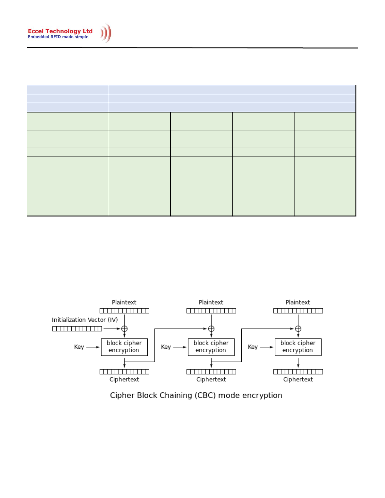
The Encrypt Data command takes as command arguments the Encryption Key Number (0x00 or 0x01), the
Initialization Vector Number (0x00 or 0x01), the Data Buffer Offset (16-bytes blocks) and the Data Length (16-bytes
blocks). This command encrypts the ‘Data Length’ number of 16-byte blocks using the AES128 CBC encryption
methodology. It operates only within the Data Buffer. This encryption method is shown in Figure 4.1.
Figure 4.1
Com mand Num ber
Com mand Name
Val i d Tag Type s
Ar gument Off set [ bytes] 0x00 0x01 0x02 0x03
Ar gument Na me
Encryption Key
Number
Initialization Vector
Number
Data Buffer Offset Data Length
Ar gument Si ze [ bytes]
0x01 0x01 0x01 0x01
Ar gument Descri ption
Number of the AES
encryption key to be
used for encryption.
Valid numbers are
0x00 and 0x01.
Number of the
Initialization Vector to
be used for encryption.
Valid numbers are
0x00 and 0x01.
Buffer offset in 16-byte
blocks from where
encryption will start.
Total data size and the
offset cannot exceed
the data buffer length.
Number of 16 byte
bocks of data to be
encrypted. This value
can be between 1 and
8.
0x08
Encrypt Data
-
Page 31

31
The Initialization Vector is used at the beginning to encrypt the first plaintext. For each subsequent 16-byte block
instead of the Initialization Vector, the algorithm uses the ciphertext output of the previous 16-byte block
encryption. The same AES Key is used for all blocks. When working with the Data Buffer during encryption the
plaintext is substituted with the corresponding ciphertext.
Page 32
32
4.2.9 Decrypt Data (0x09)
Table 4.9
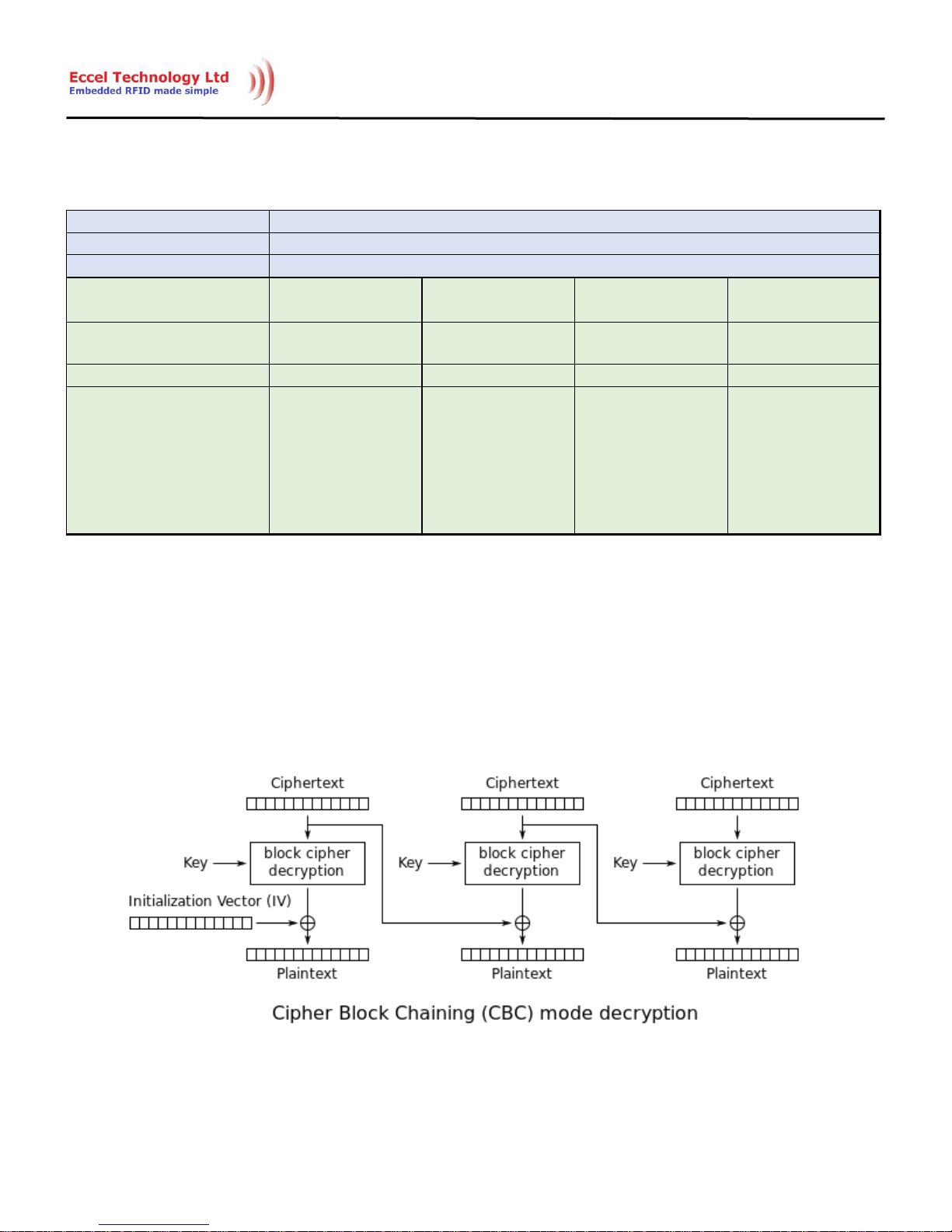
The Decrypt Data command takes as arguments the Decryption Key Number (0x00 or 0x01), the Initialization Vector
Number (0x00 or 0x01), the Data Buffer Offset (16-bytes) and the Data Length (16-bytes). This command decrypts
the ‘Data Length’ number of 16-bytes blocks using the AES128 CBC decryption methodology. It operates only within
the Data Buffer. This decryption method is shown in Figure 4.2.
Figure 4.2
Com mand Num ber
Com mand Name
Val i d Tag Type s
Ar gument Off set [ bytes] 0x00 0x01 0x02 0x03
Ar gument Na me
Decryption Key
Number
Initialization Vector
Number
Data Buffer Offset Data Length
Ar gument Si ze [ bytes]
0x01 0x01 0x01 0x01
Ar gument Descri ption
The number of the AES
Key to be used for
decryption. Valid
numbers are 0x00 and
0x01.
Number of the
initialization Vector to
be used for decryption.
Valid numbers are
0x00 and 0x01.
Buffer offset in 16-byte
blocks from where the
decryption is to start.
Total data size and the
offset cannot exceed
the data buffer length.
The number of 16-byte
blocks to be decrypted.
This value has to be
between 1 and 8.
0x09
Decrypt Data
-
Page 33

33
The Initialization Vector is used at the beginning to decrypt the first ciphertext. For each subsequent 16-byte block,
instead of the Initialization Vector, the algorithm uses the ciphertext output of the previous 16-byte block
decryption. The same AES Key is used for all blocks. When working with the Data Buffer during decryption the
ciphertext is substituted with the corresponding plaintext.
Page 34

34
4.2.10 Read Value (0x0A)
Table 4.10
The Read Value command takes as arguments the address of the block where the value is stored (Block Address), the
offset of the Data Buffer where the value and read address will be stored (Data Buffer Offset), the Authentication
Key Number and (optionally) the Authentication Key. This command has the same functionality as the Read Block
command except it treats the block as a special Value type defined by the Mifare standard. It tries to parse the block
content to this 4-byte signed value and to read a-byte address stored in last four bytes of the block. If read was
successful, the value is stored in the Data Buffer at the pointed offset, with the address byte stored straight after the
value. The value is stored as a signed 32-bit integer, with least significant byte first, and the address is stored as an
unsigned 8-bit value.
Comma nd Num ber
Comma nd Nam e
Val i d Tag Types
Ar gument Of fse t [ bytes] 0x00 0x01 0x02 0x03
Ar gument Nam e Block Address Data Buffer Offset
Authentication Key
Number
Authentication Key
Ar gument Size [ bytes]
0x01 0x01 0x01 0x06
Ar gument Descr ipti on
The Block Address in
the memory from
which the value is to be
read. The block has to
be formatted as a value
type block before
reading.
Buffer offset in bytes
from where the data
read from the tag will
be stored. Total read
size and the offset
cannot exceed the data
buffer length.
The 6 least significant
bits define the
Authentication Key
from 0 to 39 that is to
be used to read the
data. If the most
significant bit (bit 7) is
set, then the key will be
used as Key B. If bit 7
is zero, then it will be
used as Key A. If bit 6
is set, then the key will
be taken from the
following argument list
(next 6 bytes).
This optional
parameter is only used
when bit 6 of the
immediately preceding
Authentication Key
Number argument is
set. If used, this key
will be used as Key A if
bit 7 of the preceding
Authentication number
is set or as Key B if not
set. The byte order is
the least significant
byte first.
0x0A
Read Value
Mifare Classic
Page 35
35
4.2.11 Write Value (0x0B)
Table 4.11
The Write Value command takes as an argument the address of the block where to store the value (Block Address),
the signed 32-bit integer value to be stored (Value), the block address value to store in the memory block (Stored
Block Address), the Authentication Key Number and (optionally) the Authentication Key. This command has the same
functionality as the Write Block command, except that it treats the block as a special Value type as defined by the
Mifare standard. It tries to format the block content to this 4-byte signed value together with the address on the last
4 bytes of the memory.
Com m a nd Num ber
Com m a nd Na me
Va li d Tag T y pes
Ar gum e nt Offse t [ bytes] 0x00 0x01 0x05 0x06 0x07
Ar gum e nt Na m e Block Address Value Stored Block Address
Authentication Key
Number
Authentication Key
Ar gum e nt Si ze [by tes]
0x01 0x04 0x01 0x01 0x06
Ar gum e nt D e scr i pti on
Address of the block in
the memory to where
the value is to be
written. The block will
be formatted as a value
type block after
writing.
Signed 32-bit value
that is to be written to
the value block. The
least significant byte is
stored first.
8-bit unsigned value to
be stored in the last 4
bytes of the block
memory.
The 6 least significant
bits (bits 0-5) define
the Authentication Key
Number from 0 to 39
to be used to encrypt
the data. If the most
significant bit is set (bit
7), then the key will be
used as Key B, if clear
then the key will be
used as Key A. If bit 6
is set, then the key will
be taken from the
following argument list
(next 6 bytes).
Optional parameter
used when bit 6 in
Authentication Key
Number argument is
set. This Key will be
used as Key B if bit 7 in
Authentication Key
Number is set or as Key
A if bit 7 is not set. The
byte order is the least
significant byte first.
Mifare Classic
0x0B
Write Value
Page 36
36
4.2.12 Increment Value (0x0C)
Table 4.12
The Increment Value command is an operation on a value-type block as defined by the Mifare standard. It takes as
arguments the block address where the value is stored (Block Address), the signed 32-bit integer number which will
be added to the value (Delta Value), the Authentication Key Number and (optionally) the Authentication Key. The
command reads the value from the block to the volatile memory on the tag and increments it by the selected delta
value. There is no further operation done. To store the value in the same or another block, the user must execute
the Transfer Value command.
Comma nd Num ber
Comma nd Nam e
Val i d Tag Types
Ar gument Of fse t [ bytes] 0x00 0x01 0x05 0x06
Ar gument Nam e Block Address Delta Value
Authentication Key
Number
Authentication Key
Ar gument Size [ bytes]
0x01 0x04 0x01 0x06
Ar gument Descr ipti on
Address of the block in
the memory from
which the value is to be
read and incremented..
Block has to be
formatted as a value
type block before
reading.
Signed 32-bit number
to be added to the
value read from the tag
block.
The 6 least significant
bits define the
Authentication Key
Number from 0 to 39
that is to be used to
read the data. If the
most significant bit (bit
7) is set, then the key
will be used as Key B. If
it is zero it will be used
as Key A. If bit 6 is set,
then the key will be
taken from the
argument list (next 6
bytes).
Optional parameter
used when bit 6 in the
preceding
Authentication Key
Number argument is
set. This key will be
used as Key B if bit 7 of
the Authentication Key
Number is set, or as
Key A if it is zero. The
byte order is the least
significant byte first.
0x0C
Increment Value
Mifare Classic
Page 37
37
4.2.13 Decrement Value (0x0D)
Table 4.13
The Decrement Value command is an operation on a value-type block, as defined by the Mifare standard. It takes as
arguments the block address where the value is stored (Block Address), the signed 32-bit integer number which will
be subtracted from the value (Delta Value), the Authentication Key Number and (optionally) the Authentication Key.
The command reads the value from the block into the volatile memory on the tag and decrements it by the delta
value. There is no further operation done. To store the value in the same or another block, the user must execute
the Transfer Value command.
Comma nd Num ber
Comma nd Nam e
Val i d Tag Types
Ar gument Of fse t [ bytes] 0x00 0x01 0x05 0x06
Ar gument Nam e Block Address Delta Value
Authentication Key
Number
Authentication Key
Ar gument Size [ bytes]
0x01 0x04 0x01 0x06
Ar gument Descr ipti on
Address of the block in
the memory from
which the value is to be
read and incremented.
Block has to be
formatted as a value
type block before
reading.
Signed 32-bit number
to be substracted from
the value read from the
tag block.
The 6 least significant
bits define the
Authentication Key
Number from 0 to 39
that is to be used to
read the data. If the
most significant bit (bit
7) is set, then the key
will be used as Key B. If
it is zero it will be used
as Key A. If bit 6 is set,
then the key will be
taken from the
argument list (next 6
bytes).
Optional parameter
used when bit 6 in the
preceding
Authentication Key
Number argument is
set. This key will be
used as Key B if bit 7 of
the Authentication Key
Number is set, or as
Key A if it is zero. The
byte order is the least
significant byte first.
0x0D
Decrement Value
Mifare Classic
Page 38
38
4.2.14 Restore Value (0x0E)
Table 4.14
The Restore Value command is an operation on a value-type block, as defined by the Mifare standard. It takes as
arguments the block address where the value is stored (Block Address), the Authentication Key Number and
(optionally) the Authentication Key. If the block is properly formatted, then the value from the block is copied to a
volatile memory register on the tag. There is no further operation done. To store the value in the same or another
block, the user must execute the Transfer Value command.
Comm and Num ber
Comm and Nam e
Val id T ag Types
Arg um ent Off se t [bytes] 0x00 0x01 0x02
Arg um ent Na me Block Address
Authentication Key
Number
Authentication Key
Arg um ent Si ze [bytes]
0x01 0x01 0x06
Arg um ent Descr iption
Address of the block in
the memory from
which the value is to be
read. The block has to
be formatted as a value
type block before
reading.
The 6 least significant
bits define the
Authentication Key
Number from 0 to 39
that is to be used to
read the data. If the
most significant bit (bit
7) is set, then the key
will be used as Key B. If
it is zero it will be used
as Key A. If bit 6 is set,
then the key will be
taken from the
argument list (next 6
bytes).
Optional parameter
used when bit 6 in the
preceding
Authentication Key
Number argument is
set. This key will be
used as Key B if bit 7 of
the Authentication Key
Number is set, or as
Key A if it is zero. The
byte order is the least
significant byte first.
0x0E
Restore Value
Mifare Classic
Page 39
39
4.2.15 Transfer Value (0x0F)
Table 4.15
The Transfer Value command is an operation on a value-type block as defined by the Mifare standard. It takes as
arguments the block address of where to store the value (Block Address), the Authentication Key Number and
(optionally) the Authentication Key. The value from the volatile register on the tag is copied to the block. The block
is formatted as a value-type block during this operation.
Comm and Num ber
Comm and Nam e
Val id T ag Types
Arg um ent Off se t [bytes] 0x00 0x01 0x02
Arg um ent Na me Block Address
Authentication Key
Number
Authentication Key
Arg um ent Si ze [bytes]
0x01 0x01 0x06
Arg um ent Descr iption
Address of the block in
the memory to which
the value is to be
transferred. The block
is formatted as a value
type block after
execution of this
command.
The 6 least significant
bits define the
Authentication Key
Number from 0 to 39
that is to be used to
read the data. If the
most significant bit (bit
7) is set, then the key
will be used as Key B. If
it is zero it will be used
as Key A. If bit 6 is set,
then the key will be
taken from the
argument list (next 6
bytes).
Optional parameter
used when bit 6 in the
preceding
Authentication Key
Number argument is
set. This key will be
used as Key B if bit 7 of
the Authentication Key
Number is set, or as
Key A if it is zero. The
byte order is the least
significant byte first.
Mifare Classic
0x0F
Transfer Value
Page 40
40
4.2.16 Recover Value (0x10)
Table 4.16
The Recover Value command takes as arguments the address of the block where the value is stored (Block Address),
the offset of the data buffer where the value and read address will be stored (Data Buffer Offset), the Authentication
Key Number and (optionally) the Authentication Key. This command has the same functionality as the Read Value
command, except that it can be used on a block which is corrupted – it tries to recover data from a corrupted block.
The format of a value-type block allows for some bits to be corrupted and it still be possible to read and recover the
proper value. The 4-byte signed value followed by 1-byte address value is stored in the Data Buffer under the Data
Buffer Offset index.
Comma nd Num ber
Comma nd Nam e
Val i d Tag Types
Ar gument Of fse t [ bytes]
0x00 0x01 0x02 0x03
Ar gument Nam e Block Address Data Buffer Offset
Authentication Key
Number
Authentication Key
Ar gument Size [ bytes]
0x01 0x01 0x01 0x06
Ar gument Descr ipti on
Address of the block in
the memory from
which the value is to be
read. The block must
be formatted as a value
type block before
reading.
Buffer offset in bytes
from where the data
from the tag is to be
stored. Total read size
and the offset cannot
exceed the data buffer
length.
The 6 least significant
bits define the
Authentication Key
Number from 0 to 39
that is to be used to
read the data. If the
most significant bit (bit
7) is set, then the key
will be used as Key B. If
it is zero it will be used
as Key A. If bit 6 is set,
then the key will be
taken from the
argument list (next 6
bytes).
Optional parameter
used when bit 6 in the
preceding
Authentication Key
Number argument is
set. This key will be
used as Key B if bit 7 of
the Authentication Key
Number is set, or as
Key A if it is zero. The
byte order is the least
significant byte first.
0x10
Recover Value
Mifare Classic
Page 41
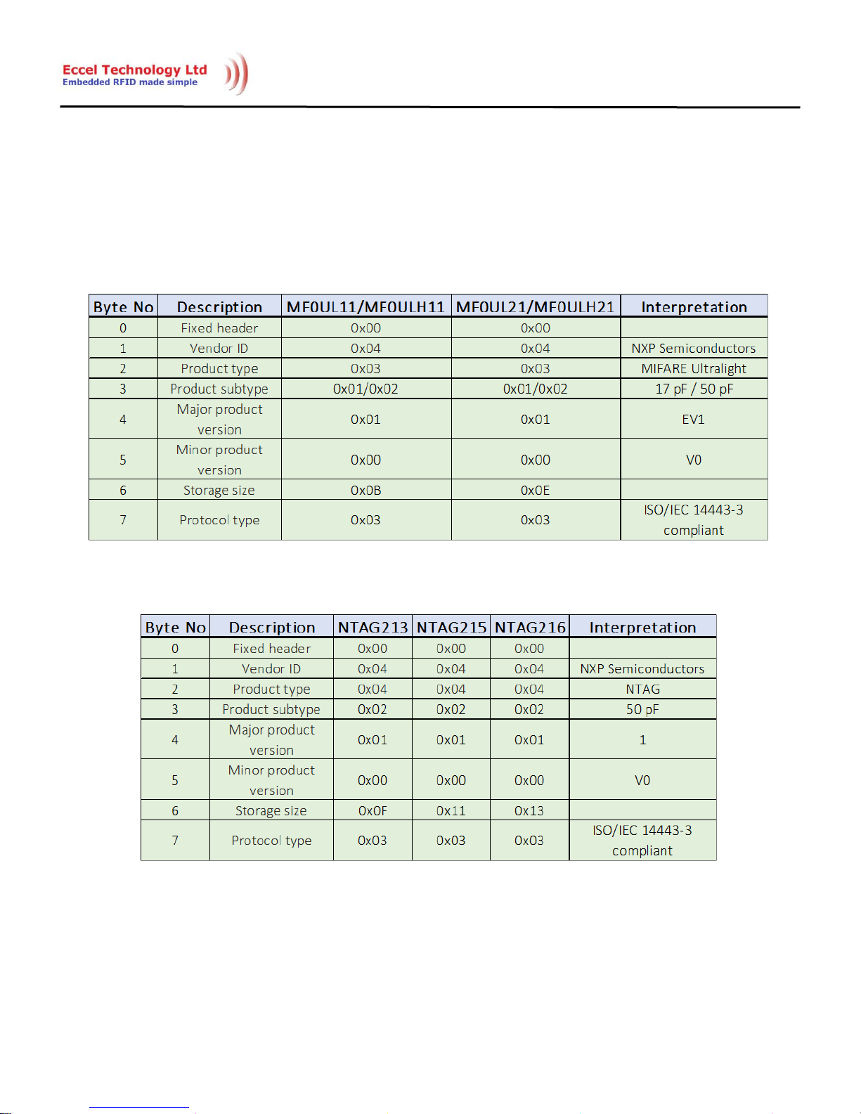
41
4.2.17 Get Version (0x11)
The Get Version command doesn’t take any arguments. This command can be used with Mifare Ultralight EV1,
NTAG213, NTAG215 and NTAG216 tags. After successful reading, the first 8 bytes in the data buffer are filled with
data defined by the NXP standard. Example are shown in Table 4.17 (Mifare Ultralight EV1) and Table 4.18 (NTAG).
Table 4.17
Table 4.18
Please refer to the NXP documentation for more information.
Page 42

42
4.2.18 Read Signature (0x12)
The Read Signature command doesn’t take any arguments. This command can be used with Mifare Ultralight EV1,
NTAG213, NTAG215 and NTAG216 tags. After successful reading, the first 32 bytes in the data buffer are filled with
the ECC signature defined by the NXP standard. Please refer to the NXP documentation for more information.
4.2.19 Configure UID (0x13)
Table 4.19
The Configure UID command takes as arguments the UID configuration byte (UID Type), the Authentication Key
Number and (optionally) the Authentication Key. This command changes the configuration of the UID on some
Mifare Classic tags. The UID Type parameter is explained in Table 4.20.
Comm and Num ber
Comm and Nam e
Val id T ag Types
Arg um ent Off se t [bytes]
0x00 0x01 0x02
Arg um ent Na me UID Type
Authentication Key
Number
Authentication Key
Arg um ent Si ze [bytes]
0x01 0x01 0x06
Arg um ent Descr iption
UID Type configuration
byte.
The 6 least significant
bits define the
Authentication Key
Number from 0 to 39
that is to be used to
read the data. If the
most significant bit (bit
7) is set, then the key
will be used as Key B. If
it is zero it will be used
as Key A. If bit 6 is set,
then the key will be
taken from the
argument list (next 6
bytes).
Optional parameter
used when bit 6 in the
preceding
Authentication Key
Number argument is
set. This key will be
used as Key B if bit 7 of
the Authentication Key
Number is set, or as
Key A if it is zero. The
byte order is the least
significant byte first.
0x13
Configure UID
Some Mifare Classic
Page 43
43
Table 4.20
UID C onfiguration Parameter Value
Descript ion
0x00
Anti-collision and selection with the double size UID.
0x01
Anti-collision and selection with the double size UID and optional
usage of a selection process shortcut.
0x02
Anti-collision and selection with a single size random ID.
0x03
Anti-collision and selection with a single size NUID where the NUID is
calculated from the 7-byte UID.
Page 44
44
4.2.20 Read Counter (0x14)
Table 4.21
The Read Counter command takes as arguments the tag Counter Number and the Data Buffer Offset in bytes. This
command reads the counter value of the counter pointed to by the Counter Number and stores it in the Data Buffer
at the Data Buffer Offset index as an unsigned 24-bit integer with the least significant byte first.
Comm and Num ber
Comm and Nam e
Val id T ag T ypes
Arg um ent Off set [bytes]
0x00 0x01
Arg um ent Na me
Counter Number Data Buffer Offset
Arg um ent Si ze [bytes]
0x01 0x01
Arg um ent Descr iption
Counter number
cannot exceed number
of counters in the tag.
Buffer offset in bytes
from where the
counter value is to be
stored. Total counter
value size and the
offset cannot exceed
the data buffer length.
0x14
Read Counter
Ultralight EV1, NTAG213, NTAG215, NTAG216,
NTAG213F, NTAG216F
Page 45
45
4.2.21 Increment Counter (0x15)
Table 4.22
The Increment Counter command takes as arguments the tag Counter Number and the Increment Value to be added
to the counter value. This command increments the counter value of the counter pointed to by the Counter
Number. The Increment Value is a 24-bit unsigned number with the least significant byte first.
Comm and Num ber
Comm and Nam e
Val id T ag T ypes
Arg um ent Off set [bytes]
0x00 0x01
Arg um ent Na me
Counter Number Increment Value
Arg um ent Si ze [bytes]
0x01 0x03
Arg um ent Descr iption
Counter number
cannot exceed number
of counters in the tag.
24-bit unsigned integer
value which will be
added to the counter
value. Byte order is
least significant byte
first.
Ultralight EV1
0x15
Increment Counter
Page 46
46
4.2.22 Check Tearing Event (0x16)
Table 4.23
The Check Tearing Event command takes as arguments the tag Counter Number and the Data Buffer Offset in bytes.
This command checks whether there was a tearing event in the counter and stores the flag value in the Data Buffer
at the Data Buffer Offset index. The value ‘0x00’ is stored if there has been no tearing event, and ‘0x01’ is stored if a
tearing event occurred.
Comm and Num ber
Comm and Nam e
Val id T ag Types
Arg um ent Off set [by tes]
0x00 0x01
Arg um ent Na me
Counter Number Data Buffer Offset
Arg um ent Si ze [bytes]
0x01 0x01
Arg um ent Descr iption
Counter number
cannot exceed number
of counters in the tag.
Buffer offset in bytes
where the check result
will be stored. Offset
cannot exceed the
buffer size.
0x16
Check Tearing Event
Ultralight EV1
Page 47
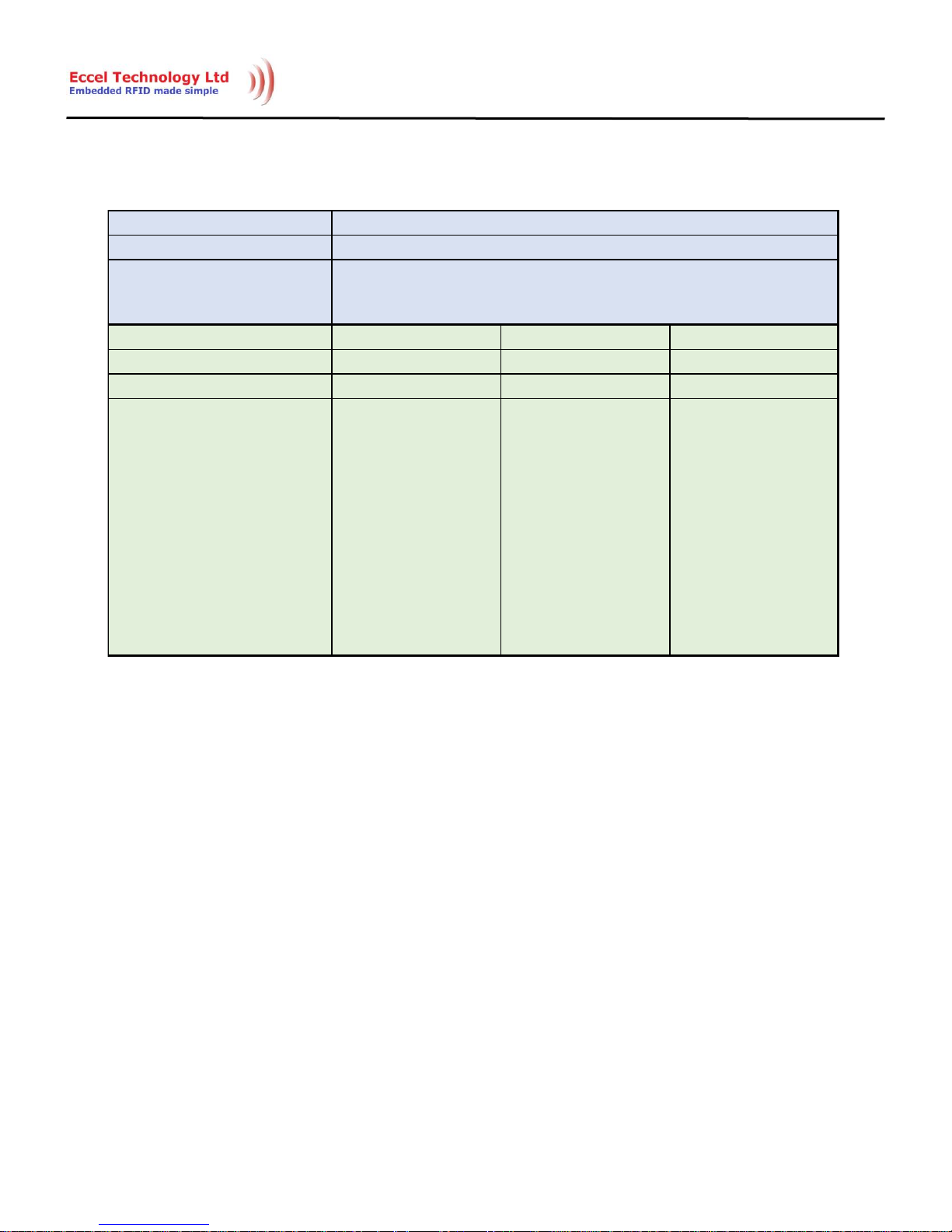
47
4.2.23 Password Authentication (0x17)
Table 4.24
The Password Authentication command takes as arguments the Data Buffer Offset where the PACK result will be
stored, the Password Number and (optionally) the Password. This command tries to authenticate the tag using the
chosen (pointed to) password. The 2-byte PACK result is stored in the Data Buffer under Data Buffer Offset index.
Comm and Num ber
Comm and Nam e
Val id T ag Types
Arg um ent Off se t [bytes]
0x00 0x01 0x02
Arg um ent Na me
Data Buffer Offset Password Number Password
Arg um ent Si ze [bytes]
0x01 0x01 0x04
Arg um ent Descr iption
Buffer offset in bytes
where the PACK result
will be stored. Offset
cannot exceed the
buffer size.
The 6 least significant
bytes define the
Password Number for
0 to 39 that is to be
used to authenticate. If
the value is equal to
0x80 the password will
be taken from next
four bytes of the
command parameters.
An Optional parameter
to be used when the
preceding password
number is set to 0x80.
The byte order is the
least significant byte
first.
0x17
Password Authentication
Ultralight EV1, NTAG210, NTAG212, NTAG213, NTAG215, NTAG216,
NTAG213F, NTAG216F
Page 48
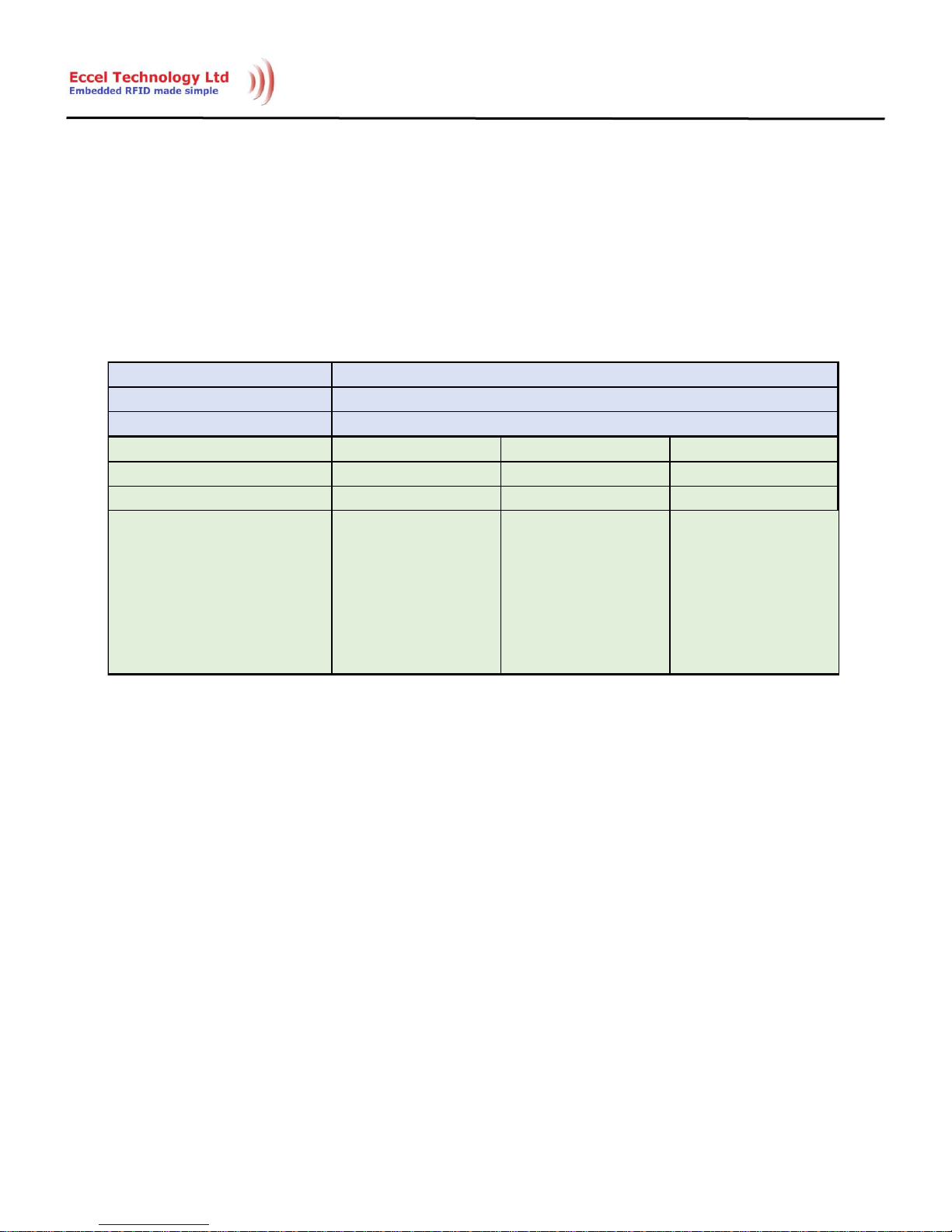
48
4.2.24 Halt (0x18)
The Halt command takes no arguments. It halts the tag and turns off the RF field. It must be executed at the end of
each operation on a tag to disable the antenna and reduce the power consumption.
4.2.25 Calculate CRC (0x19)
Table 4.25
The Calculate CRC command takes as arguments the Memory Address, the Data Length in bytes and the Data Buffer
Offset. The CRC calculation starts at the byte pointed at by the memory address and is done on the ‘Data Length’
number of bytes in the volatile memory. The result is stored in the Data Buffer at the Data Buffer Offset index. The
result is a 16-bit unsigned value with least significant byte first. The CRC calculation code is shown below.
static const uint16_t CCITTCRCTable [256] = {
0x0000, 0x1021, 0x2042, 0x3063, 0x4084, 0x50a5,
0x60c6, 0x70e7, 0x8108, 0x9129, 0xa14a, 0xb16b,
0xc18c, 0xd1ad, 0xe1ce, 0xf1ef, 0x1231, 0x0210,
0x3273, 0x2252, 0x52b5, 0x4294, 0x72f7, 0x62d6,
0x9339, 0x8318, 0xb37b, 0xa35a, 0xd3bd, 0xc39c,
0xf3ff, 0xe3de, 0x2462, 0x3443, 0x0420, 0x1401,
0x64e6, 0x74c7, 0x44a4, 0x5485, 0xa56a, 0xb54b,
0x8528, 0x9509, 0xe5ee, 0xf5cf, 0xc5ac, 0xd58d,
0x3653, 0x2672, 0x1611, 0x0630, 0x76d7, 0x66f6,
0x5695, 0x46b4, 0xb75b, 0xa77a, 0x9719, 0x8738,
0xf7df, 0xe7fe, 0xd79d, 0xc7bc, 0x48c4, 0x58e5,
Comm and Num ber
Comm and Na me
Val id T ag Types
Arg um ent Off set [bytes]
0x00 0x02 0x04
Arg um ent Na me
Memory Address Data Length Data Buffer Offset
Arg um ent Si ze [bytes]
0x02 0x02 0x01
Arg um ent D escr ipti on
Byte address in the
memory from which
the CRC calculation is
to start. This is an
unsigned 16-bit value
with least significant
byte first.
Data length in bytes
upon which the CRC is
to be performed. This
is an unsigned 16-bit
value with least
significant byte first.
Buffer offset in bytes
where the CRC value is
to be stored. The CRC
value is 16-bit
unsigned with least
significant byte first.
0x19
Calculate CRC
-
Page 49

49
0x6886, 0x78a7, 0x0840, 0x1861, 0x2802, 0x3823,
0xc9cc, 0xd9ed, 0xe98e, 0xf9af, 0x8948, 0x9969,
0xa90a, 0xb92b, 0x5af5, 0x4ad4, 0x7ab7, 0x6a96,
0x1a71, 0x0a50, 0x3a33, 0x2a12, 0xdbfd, 0xcbdc,
0xfbbf, 0xeb9e, 0x9b79, 0x8b58, 0xbb3b, 0xab1a,
0x6ca6, 0x7c87, 0x4ce4, 0x5cc5, 0x2c22, 0x3c03,
0x0c60, 0x1c41, 0xedae, 0xfd8f, 0xcdec, 0xddcd,
0xad2a, 0xbd0b, 0x8d68, 0x9d49, 0x7e97, 0x6eb6,
0x5ed5, 0x4ef4, 0x3e13, 0x2e32, 0x1e51, 0x0e70,
0xff9f, 0xefbe, 0xdfdd, 0xcffc, 0xbf1b, 0xaf3a,
0x9f59, 0x8f78, 0x9188, 0x81a9, 0xb1ca, 0xa1eb,
0xd10c, 0xc12d, 0xf14e, 0xe16f, 0x1080, 0x00a1,
0x30c2, 0x20e3, 0x5004, 0x4025, 0x7046, 0x6067,
0x83b9, 0x9398, 0xa3fb, 0xb3da, 0xc33d, 0xd31c,
0xe37f, 0xf35e, 0x02b1, 0x1290, 0x22f3, 0x32d2,
0x4235, 0x5214, 0x6277, 0x7256, 0xb5ea, 0xa5cb,
0x95a8, 0x8589, 0xf56e, 0xe54f, 0xd52c, 0xc50d,
0x34e2, 0x24c3, 0x14a0, 0x0481, 0x7466, 0x6447,
0x5424, 0x4405, 0xa7db, 0xb7fa, 0x8799, 0x97b8,
0xe75f, 0xf77e, 0xc71d, 0xd73c, 0x26d3, 0x36f2,
0x0691, 0x16b0, 0x6657, 0x7676, 0x4615, 0x5634,
0xd94c, 0xc96d, 0xf90e, 0xe92f, 0x99c8, 0x89e9,
0xb98a, 0xa9ab, 0x5844, 0x4865, 0x7806, 0x6827,
0x18c0, 0x08e1, 0x3882, 0x28a3, 0xcb7d, 0xdb5c,
0xeb3f, 0xfb1e, 0x8bf9, 0x9bd8, 0xabbb, 0xbb9a,
0x4a75, 0x5a54, 0x6a37, 0x7a16, 0x0af1, 0x1ad0,
0x2ab3, 0x3a92, 0xfd2e, 0xed0f, 0xdd6c, 0xcd4d,
0xbdaa, 0xad8b, 0x9de8, 0x8dc9, 0x7c26, 0x6c07,
0x5c64, 0x4c45, 0x3ca2, 0x2c83, 0x1ce0, 0x0cc1,
0xef1f, 0xff3e, 0xcf5d, 0xdf7c, 0xaf9b, 0xbfba,
0x8fd9, 0x9ff8, 0x6e17, 0x7e36, 0x4e55, 0x5e74,
0x2e93, 0x3eb2, 0x0ed1, 0x1ef0 };
static uint16_t GetCCITTCRC(const uint8_t* Data, uint32_t Size) {
uint16_t CRC;
uint16_t Temp;
uint32_t Index;
if (Size == 0) {
return 0;
}
CRC = 0xFFFF;
for (Index = 0; Index < Size; Index++){
Temp = (uint16_t)( (CRC >> 8) ^ Data[Index] ) & 0x00FF;
Page 50
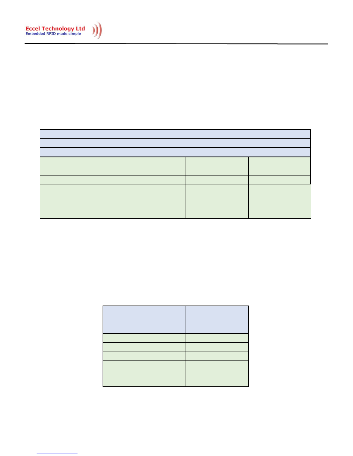
50
CRC = CCITTCRCTable[Temp] ^ (CRC << 8);
}
return CRC;
}
4.2.26 Copy Data (0x1A)
Table 4.26
The Copy Data command copies data around inside the RFID Module memory. This command takes as arguments
the Destination Address, the Source Address and the Data Length in bytes.
4.2.27 Unlock (0x1B)
Table 4.27
Comm and Num ber
Comm and Na me
Val id T ag Types
Arg um ent Off set [bytes]
0x00 0x02 0x02
Arg um ent Na me
Destination Address Source Address Data Length
Arg um ent Si ze [bytes]
0x02 0x02 0x02
Arg um ent D escr i pti on
The address in the
memory to where the
data is to be copied.
The address in the
memory from where
the data is to be
copied.
Size of the copied data
in bytes.
-
0x1A
Copy Data
Comm and Num ber
0x1B
Comm and Na me
Unlock
Val id T ag Types -
Arg um ent Off set [byte s]
0x00
Arg um ent Na me
Password
Arg um ent Si ze [bytes]
0x08
Arg um ent Descr iption
8-byte long password
with the least
significant byte first.
Page 51

51
The Unlock command takes as an argument an 8-bytes long password. If the password matches the actual password
in the module the memory which contains:
- AES Initialization Vectors
- AES Encryption Keys
- Authentication Keys and Passwords
- User Memory
- Password
will be unlocked and made accessible for read and write operations.
4.2.28 Lock (0x1C)
This Function takes no arguments. If the device is unlocked and the user executes the Lock command, protected
memory which contains:
- AES Initialization Vectors
- AES Encryption Keys
- Authentication Keys and Passwords
- User Memory
- Password
will be saved to non-volatile memory and locked (direct access will be blocked).
4.2.29 Get Module Version (0x1D)
The Get Module Version command takes no arguments. After execution, the Data Buffer at index 0x00 is filled with a
NULL-ended ASCII string which describes the hardware and firmware version of the module.
4.2.30 Reset to Default (0x1E)
The Reset to Default command doesn’t take any arguments. It resets all memory including protected memory to
factory default settings. All locked information is lost.
Page 52

52
4.3 Power Down Mode
The Power Down functionality is provided via the nPWRDN pin. This pin is configured as an input without any pull-up
or pull-down resistors, thus it must be driven by the user. For normal operation, this pin should be connected to VCC
or driven high. After the user drives this pin low the system prepares to go into Power Down Mode and drives nBUSY
line low just before entering this state. To wake up module the nPWRDN pin must be driven high. The module will
restart and drive the nBUSY line low to inform the user that it is starting the system again. When start-up is
completed, the nBUSY line is driven high. During the restart, none of the volatile memory content is retained.
The reaction time of the system will vary depending upon the active configuration and the following:
Communication – if the line is pulled low whilst there is ongoing communication, then the Power Manager
will wait until communication is finished before going into the Power Down state.
Command execution – if the line is pulled low whilst the system is executing a command, then the Power
Manager will wait until command execution is finished before going into the Power Down state.
When the module is in the Power Down state, all systems are turned-off and all IOs are in a high impedance state.
The module won’t respond to any signals or communication coming from outside.
4.4 Memory Locking
The module has an option to lock its memory using an 8-byte long password. The default state of the module after
power-up is locked and the default password is all bytes equal to 0x00. The user cannot see the memory content
when the module is locked, and any write to the memory will be discarded. During the unlock procedure, the
content of the non-volatile memory is copied to the volatile memory and is available for reading and writing.
Changes made in volatile memory are updated in non-volatile memory during the lock procedure. Commands using
data from this memory range use the volatile memory when the module is unlocked and non-volatile memory when
the module is locked
Page 53

53
5 Communication Interface
5.1 nBUSY line
The RFID A1 Module provides two communication buses: SPI Slave and I2C Slave. Each of these buses has an equal
level of access to the module internal registers. These buses operate independently but the user cannot use both at
the same time. The module has no safety system and doing so can make the system work in unpredictable ways.
The RFID A1 Module provides nBUSY signal line which shares the functionality between both communication buses.
This signal line is configured as an output. The nBUSY signal is driven low by the module when anything is written to
the memory. At the same time when nBUSY line is driven low the result register is set to 0xFF value. This inform the
user that module is busy and is parsing data or executing command and nothing else should be written to the
module now. The user must wait for nBUSY line going high or Result Register value changing from 0xFF to perform
any operation on the module or to read any data from the module which is a result of current processing.
5.2 SPI Bus
The RFID A1 Module provides a SPI slave bus. This is one of two buses provided by the module. It is the fastest
communication option in the module. The high clock frequency together with simultaneous communication in both
directions gives the fastest data exchange rate, but requires the most number of IO lines.
5.2.1 Bus signals and timings requirements
There are four signals necessary for communication via SPI bus. These are CLK, MOSI, MISO and CS. CLK (Clock), CS
(Chip Select) and MOSI (Master Out Slave In) signals are controlled by the master on every transmission and these
pins on the RFID A1 module are configured as inputs without any pull-up or pull-down resistors. MISO (Master In
Slave Out) signal is driven by the module to Vcc and to ground when there is ongoing transmission. During
communication via the SPI bus the user must pay attention to the nBUSY signal or must be sure that the Result
Register has other value than 0xFF when writing to the module.
The SPI frame timing together with clock polarisation and phase is shown in Figure 5.1.
Page 54
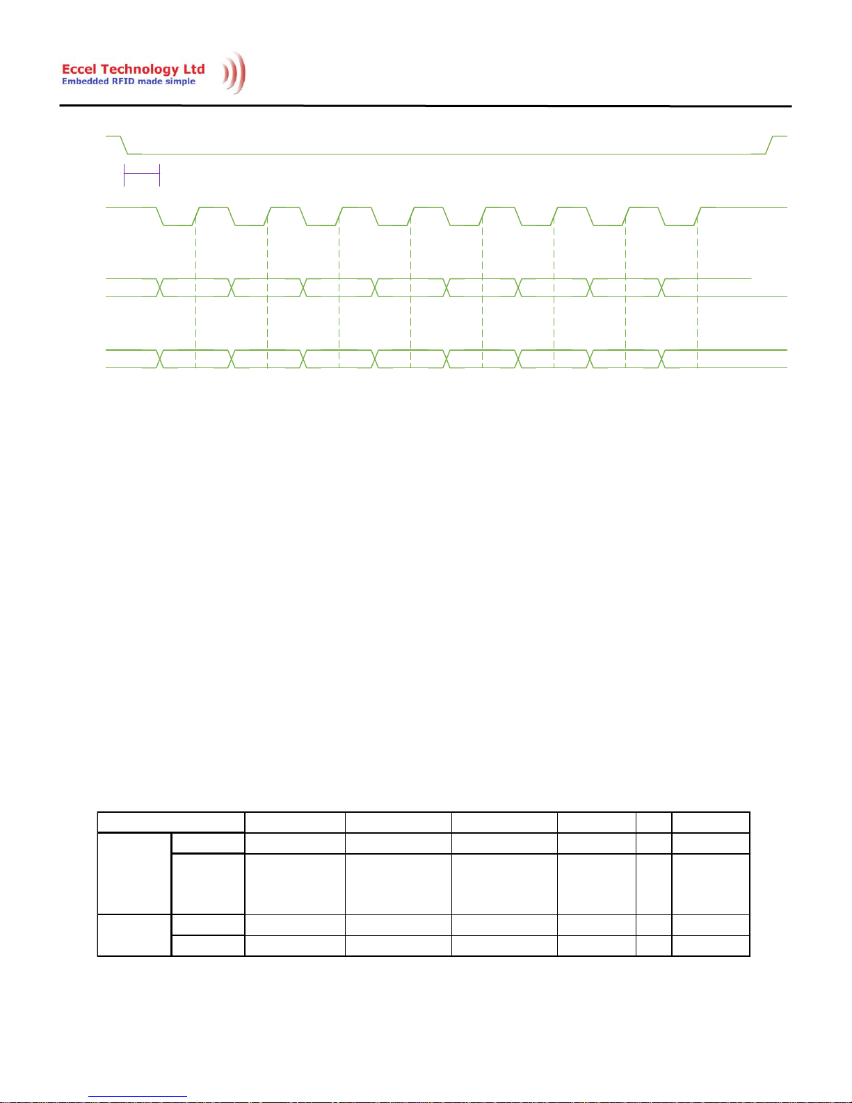
54
CS
CLK
MOSI
MISO
CLK1 CLK2 CLK3 CLK4 CLK5 CLK6 CLK7 CLK8
B7
B7
B6
B6
B5
B5
B4
B4
B3
B3
B2
B2
B1
B1
B0
B0
T1
Figure 5.1
As Figure 5.1 shows the clock idle state is high. On a falling edge of the clock the module switches the state of the
data line (MISO) and on a rising edge of the clock the module samples the data line (MOSI). During transmission, the
most significant bit is transmitted first. One frame is eight bits long (one byte). The CS signal is active low thus the
master must drive the CS signal low before clocking the clock signal. The maximum clock frequency for the system is
500 kHz. An additional restriction is also placed on the minimum allowed time between the CS line going low and
the first clock falling edge and the minimum allowed time for CS being high between transmission (please see
chapter 2.7). This is the result of low power consumption as the system must jump from sleep state to run state at
various points during communication.
5.2.2 Exchanging data (reading or reading and writing)
The SPI bus is a type of synchronous bus where both sides (master and slave) synchronised by the master clock send
data at the same time in both directions. Each transmission is initiated when the master drives the CS line low and
ends when the CS line is driven high. All bytes transmitted in each direction between falling and rising edge of the CS
line are considered as one packet and bytes within those packets are ordered. The First byte is transmitted always
after the falling edge of the CS signal. A typical packet exchange is shown in Table 5.1.
Table 5.1
1 2 3 4 3 + n
Value 0x00 - 0xFF 0x00 - 0xFF 0x00, 0x01 0x00 - 0xFF 0x00 - 0xFF
Type Address LSByte Address MSByte
0x00 - Read,
0x01 - Read and
Write
Data Byte 1 …….. Data Byte n
Value 0x00 - 0xFF 0x00 - 0xFF 0x00 - 0xFF 0x00 - 0xFF 0x00 - 0xFF
Type Trash data Trash data Trash data Data Byte 1 …….. Data Byte n
Byte number
MOSI
MISO
Page 55
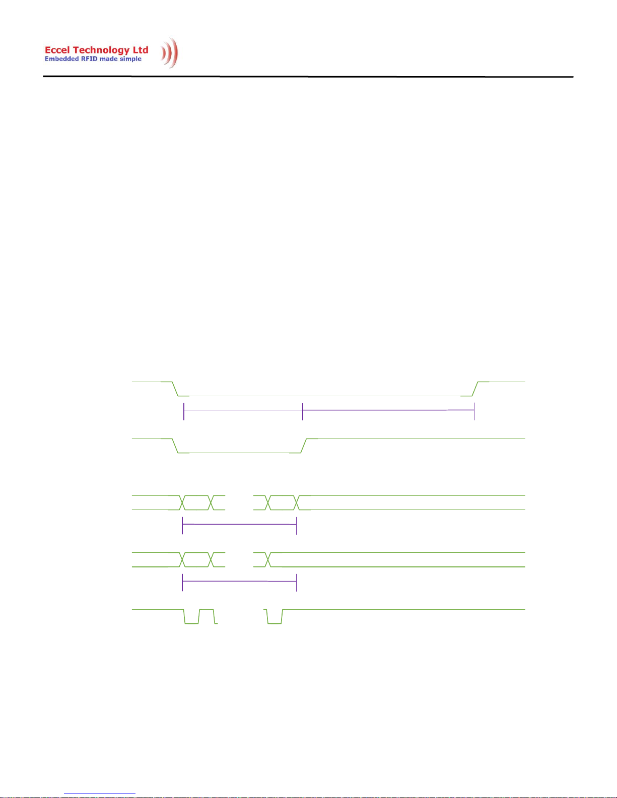
55
When the CS signal goes low the byte index resets. The first three bytes transmitted from the module (MISO line)
are trash and should be discarded by the master. The first three bytes transmitted from the master (MOSI line) are
used to set up the transmission starting from byte four onwards. The first byte is the least significant byte of the
address to where to write to or from where to read the data. The second byte is the most significant byte of the
address. The address is represented as an unsigned 16-bit number. The third byte is the write indicator flag. If the
master wants the data sent via the MOSI line to be written to the module’s registers, then the third byte in the
packet should have the value ‘0x01’. If the master sets this byte to value ‘0x00’, then the RFID A1 module will discard
incoming data (will not store them) and just stream the data on the MISO line from the RFID A1 memory.
5.2.3 Command processing
The RFID A1 module after CS goes high (end of communication) starts to process the data. Even if the master didn’t
write anything to the memory and just read data from the module, it will still drive the nBUSY line low for a while to
do internal housekeeping. A typical communication timing is shown below in Figure 5.2.
nBUSY
MOSI ...
Data sent from master
Command execution
CS
MISO ...
Data sent from slave
CLK ...
Data exchange
Figure 5.2
Page 56
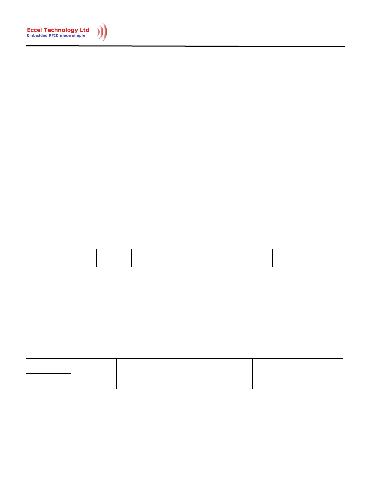
56
5.3 I2C Bus
The RFID A1 Module provides a I2C slave bus. The advantages of the I2C are that it requires only two lines to
communicate and that multiple devices can be connected to the 2-wire same bus.
The implementation of I2C in the module complies with the 7-bit addressing I2C standard, thus the timing diagrams
for bit and frame representation will be omitted in this document. Each transmission on the I2C line begins with an
I2C START condition and ends with an I2C STOP condition. In between these events there could be as many repeated
STARTs as the user wants. The behaviour of the nBUSY line is the same for all buses, thus as well for I2C. The
module starts processing the command after receiving a stop condition on I2C bus.
5.3.1 I2C Address Construction
After reset or power-up when the module starts, it samples three IO lines (I2C AD0, I2C AD1 and I2C AD2) to
construct the I2C address to which it will respond. Thanks to this solution there is the possibility to connect to eight
such modules on one I2C bus. Byte wise the address sent on the I2C bus after START is constructed as follows:
Table 5.2
5.3.2 Writing to the memory
Writing to the RFID A1 Module memory via the I2C bus is very similar to other memory type devices. A typical
transmission for writing to the registers is shown below in Table 5.3.
Table 5.3
Bit number 7 6 5 4 3 2 1 0
Value 0 1 0 0 Sampled from AD2 Sampled from AD1 Sampled from AD0 -
Type Address bit 6 Address bit 5 Address bit 4 Address bit 3 Address bit 2 Address bit 1 Address bit 0 Read / Write bit
Byte number 1 2 3 4 3 + n
Value I2C Address + 0x00 0x00 - 0xFF 0x00 - 0xFF 0x00 - 0xFF 0x00 - 0xFF
Type
START + I2C
address + Write
Address LSByte Address MSByte Data Byte 1 …….. Data Byte n + STOP
Page 57
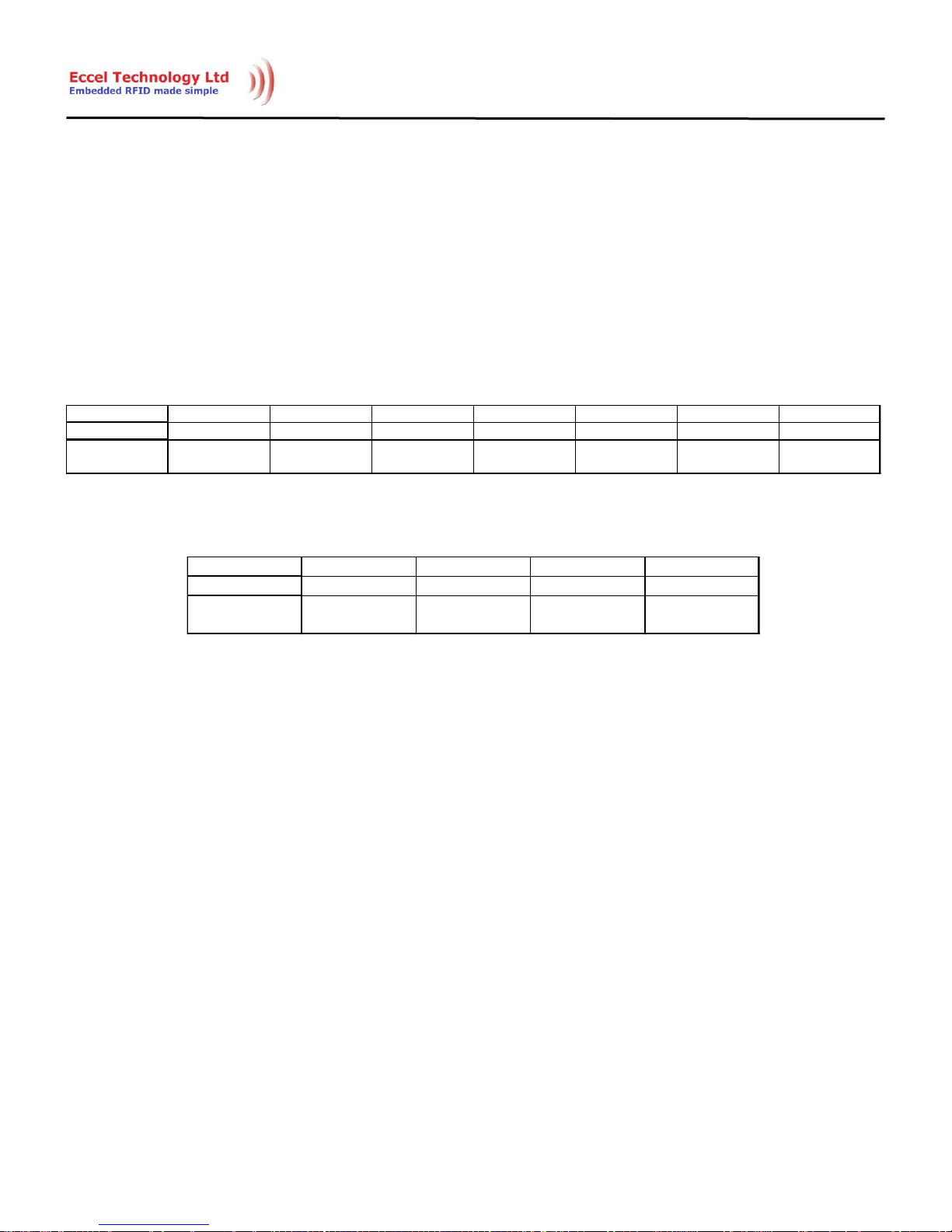
57
The master must initiate the transmission on the I2C bus by sending a START condition followed by the I2C address of
the slave device with R/W byte set to 0. The second and third byte sent by the master will set up the address index
under which the data will be stored. Starting from the fourth byte the data will be stored under the passed address
value and the memory index will be automatically increased by one each time. When the RFID A1 module recognizes
its I2C address it drives the nBUSY line low to inform the master that it is receiving the data.
5.3.3 Reading from the memory
The master can read from the module in two possible ways presented below in Table 5.4 and Table 5.5.
Table 5.4
Table 5.5
As shown in Table 5.4, to read from a certain address the master first must write the address index by sending a
START condition followed by the I2C address to be written and two bytes representing the index. Later and without
sending a STOP condition the master must send a repeated START signal, this time followed by the I2C address to be
read. Bytes after the I2C read address will be transmitted from the module and will contain memory data starting
from the address index set up by the master at the beginning of the transmission. The index is automatically
increased and stored between transmissions. If the user wants to continue reading data starting from the index
value left since last transmission, he can use the simplified version of the transmission shown in Table 5.5.
Byte number 1 2 3 4 5 5 + n
Value I2C Address + 0x00 0x00 - 0xFF 0x00 - 0xFF I2C Address + 0x01 0x00 - 0xFF 0x00 - 0xFF
Type
START + I2C
address + Write
Address LSByte Address MSByte
START + I2C
address + Read
Data Byte 1 …….. Data Byte n + STOP
Byte number 1 2 2 + n
Value I2C Address + 0x01 0x00 - 0xFF 0x00 - 0xFF
Type
START + I2C
address + Read
Data Byte 1 …….. Data Byte n + STOP
Page 58
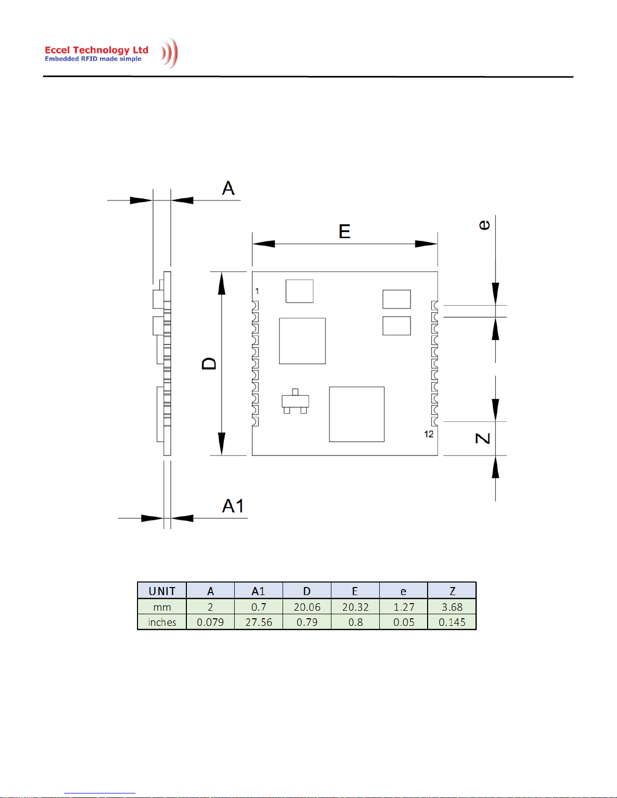
58
6 Mechanical
6.1 Dimensions
Drawing 1
Table 6.1
Page 59
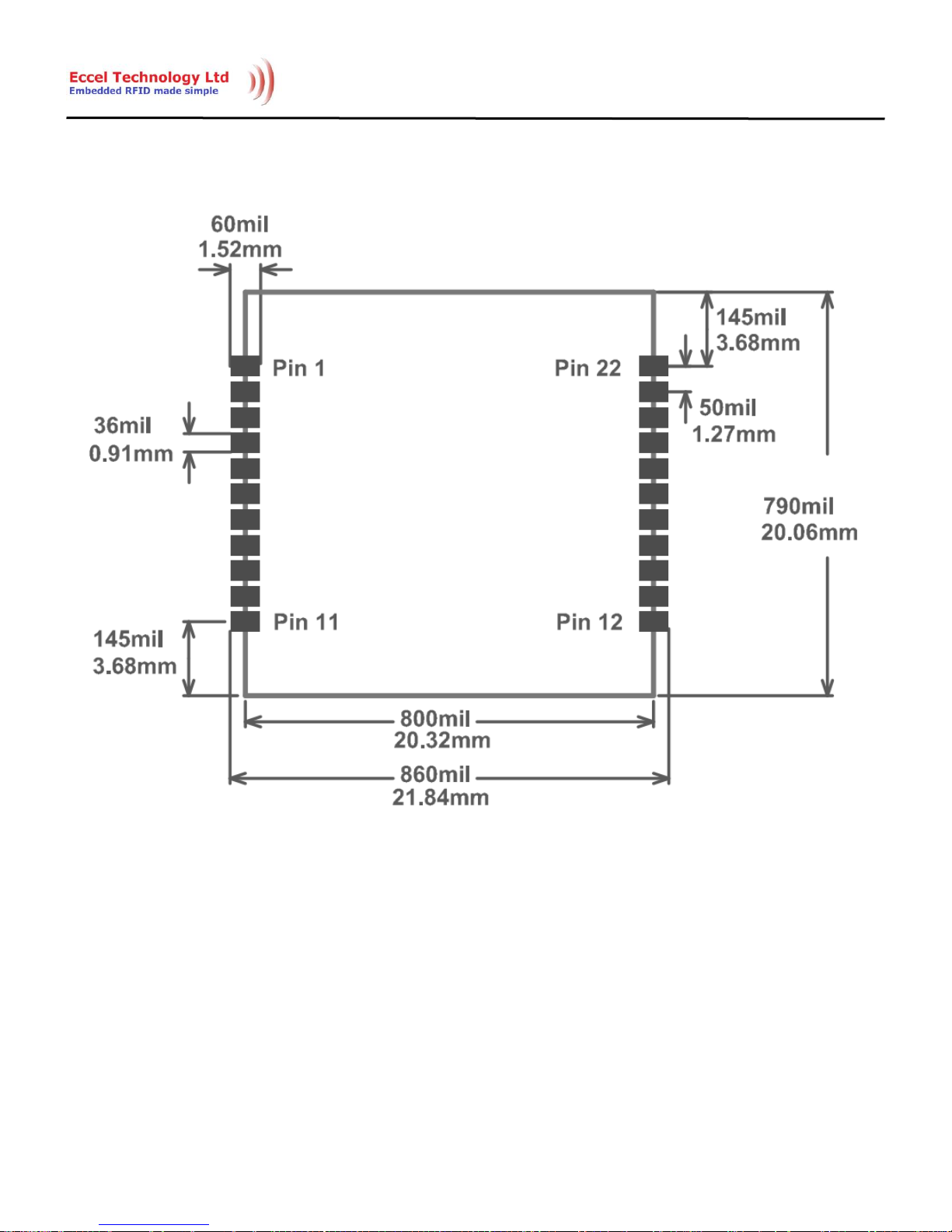
59
6.2 Recommended Footprint
Drawing 2
Page 60

60
 Loading...