

ESS ES2842S Datasheet

ESS Technology, Inc. SAM0388-041101 1
ESS Technology, Inc.
ES2842
PCI Integrated LAN V.90/V.92 Modem Solution
Product Brief
DESCRIPTION
The ES2842, ESS Technology’s first LAN plus host-based
TeleDrive modem chip for the PCI bus, provides desktop
and notebook computers with greater connectivity to both
packet networks and telephone networks. The ES2842
maximizes integration and reduces the external component
BOM cost to a minimum.
The ES2842 device combines into a single-chip a host-based
V.90/V.92 modem, modem control buffers, a modem codec, and
an IEEE 802.3-compatible Ethernet media access controller
(MAC) with an analog phoneline interface and a PCI bus
interface. This advanced high-level device integration allows the
ES2842 to be used as a host-based modem and LAN solution for
desktop and notebook systems requiring either a modem
connection or a 10/100 Ethernet connection. The ES2842 is also
capable of providing a home network connection that complies
with the Home Phoneline Networking Alliance (HomePNA) 1-Mb/
s (HPNA1.0) specification.
The ES2842 LAN feature supports 100BASE-TX (100-Mb/s
mode) and 10BASE-T (10-Mb/s mode) full-duplex operations.
The ES2842 includes a media-independent interface (MII) and
reduced MII (RMII), enabling it to interface with an external PHY
transceiver used for either a LAN or HPNA-based chipset.
The ES2842 modem sends and receives data and fax
information and supports the telephone answering machine
(TAM) feature. With its built-in ACPI D3
cold
wake-on-LAN and
wake-on-ring support, the ES2842 is an ideal modem solution for
notebooks and battery-operated devices. The ES2842 modem
provides the interface and control logic needed to transfer data
between its serial I/O terminals and the PCI interface.
The ES2842 delivers a high modem connectivity rate, as well as
high throughput without the need of a dedicated DSP. The
ES2842 supports worldwide homologation and is capable of
data/fax/voice call discrimination. With the addition of an external
transformer DAA, the ES2842 provides a very cost-effective
modem/LAN solution for add-on card, motherboard, and miniPCI card implementations.
The ES2842 is available in a 128-pin low-profile quad flat pack
(LQFP) package.
FEATURES
• V.90/V.92 analog data/fax/TAM modem
• Data mode capabilities:
—– V.90/V.92: 56 kbps
—– ITU-T V.34: 33.6 kbps and fallbacks
• Fax mode capabilities:
—– ITU-T V.17, V.29, V.27ter, and V.21ch2
—– Group 3 (TIA/EIA-578 Class 1 and Class 2)
• Requires minimum 166-MHz Pentium with MMX technology
• Integrated modem codec and analog front end
• 16-bit ADC and DAC with built-in anti-aliasing and
reconstruction filters
• Supports external transformer DAA
• 10/100-Mb/s LAN or 1-Mb/s HPNA networking capability
• Integrated on-chip 1/10/100-Mbps MAC controller capable of
interfacing with 10Base-T PHY transceiver and with 100BaseTX PHY transceiver
• MII for connecting to external 10/100-Mbps PHY transceiver
• RMII for connecting to external 10/100-Mbps PHY transceiver
• Full-duplex operation supported in MII and RMII ports with
independent transmit (TX) and receive (RX) channels
• Support for IEEE 802.3x flow control and IEEE 802.3u auto-
negotiation for 10Base-T and 100Base-TX
• EEPROM interface for subsystem ID and subsystem vendor ID
• ACPI and PCI power management standard-compliant
• Wake-on-ring and wake-on-LAN capability
• On-chip FIFOs for PCI bus and both RX and TX state machines
• Supports both RJ-11 tip and ring connection and RJ-45 LAN/
Ethernet connection
• PC99/PC2001-compliant with support for V.250, V.251, and
V.253 commands
• Worldwide homologation
MODEM DRIVER SUPPORT
•
Microsoft Windows 98/SE/ME/2000
• Microsoft Windows NT 4.0
LAN DRIVER SUPPORT
•
NIC drivers for Netware 3.x and 4.x networks (16-bit and
32-bit ODI)
• Microsoft Windows networks (NDIS 2.0, 4.0, and 5.0)
• Packet driver
• Linux
2 SAM0388-041101 ESS Technology, Inc.
ES2842 PRODUCT BRIEF
PINOUT
PINOUT
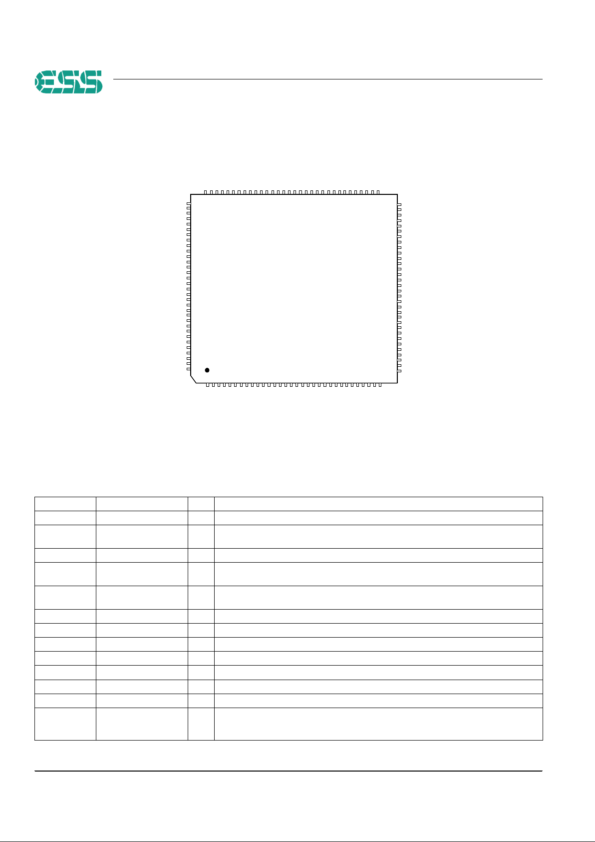
Figure 1 shows the ES2842 pinout diagram.
Figure 1 ES2842 Pinout Diagram
PIN DESCRIPTIONS
Table 1 lists the ES2842 pin descriptions.
1
DSPK
PF10
PF9
PF8
NC
OSCO
VCM
VREF
RXN
NC
NC
NC
NC
TXCLK/REFCLK
RXD1
RXD2
VAUX
RXD0
RXER/RX_ER
RXDV/CRS_DV
COL/SPEED10
GND
MDIO/SECLK
MDC/RMII_MODE
RXD3
SECS
RING_IN
TXN
TXP
AGND
AVDD
PF2
PF3
PF4
PF5
TRIDRV
GND
OSCI
LINK_ST2
PWR_RSTB
RST_PHYB
NC
NC
AD16
AD17
AD18
AD19
AD21
AD22
AD23
GND
IDSEL
CBE3#
VDD
AD24
AD25
AD28
AD26
AD27
AD29
AD30
AD31
AD3
CBE0#
AD4
IRDY#
GND
FRAME#
CBE2#
VDD
96
97
64
AD6
AD7
VDD
AD8
AD9
AD10
AD11
AD12
AD13
AD14
AD15
33
32
GND
CBE1#
PAR
STOP#
DEVSEL#
TRDY#
PME#
VAUXP/WOL
PCICLK
CLKRUN#
PCIGNT#
PCIREQ#
RST#
INTA#
128
VAUX
GND
D1
TXEN
TXD2
65
AD20
AD5
RXP
NC
NC
AD0
AD1
AD2
GND
VAUX
GND
RXCLK
IRQ#
CRS
LINK_ST1
VAUX
PF7
VDD
GND
SERR#
GND
VDD
VDD
GND
SEDO/TXD0
SEDI/TXD1
TXD3
VAUX
ES2842S
128-Pin LQFP
Table 1 ES2842 Pin Descriptions
Names Pin Numbers I/O Definitions
IDSEL 1 I ID select.
GND 2, 3, 22, 23, 52, 53, 72,
85, 86, 116, 117
G Digital ground.
VDD 12, 13, 37, 38, 126, 127 P 3.3V digital power supply.
AD[31:0] 4:11, 24:28, 33:35,
39:46, 118:125
I/O Address and data lines from the PCI bus.
C/BE[3:0]# 14, 21, 36, 128 I/O PCI command/byte enable. During address phase of a transaction, these pins define the bus com-
mand. During data phase, these pins define the bus enable.
FRAME# 15 I/O Cycle frame.
IRDY# 16 I/O Initiator ready.
TRDY# 17 I/O Target ready.
DEVSEL# 18 I/O Device select.
STOP# 19 I/O Stop transaction.
PAR 20 I/O Parity.
SERR# 29 OD System bus error.
PF[10:7] and
PF[5:2]
30:32, 47:51 I/O General-purpose programmable bidirectional flag. These pins can be used for interfacing with a tele-
phone or other device, performing such functions as caller ID, etc. Refer to pin
descriptions of pins 54, 108, and 109 for preprogrammed telephone interface pins.
 Loading...