

Page 1

Wi-Fi& Bluetooth Internet of Things Module
RIGEL
Datasheet
Including:
W11261889
Version 1.3
Espressif Systems
Copyright © 2018
www.espr
essif.com
Page 2

This document introduces the specifications of RIGEL REV C.
Release Notes
About This Document
Date Version Release notes
2018.05
2018.10 V1.1
2018.08 V1.2
2018.10 V1.3
2018.11 V1.4 Added information on PCB antennas in Chapter 1.
V1.0 First release.
Updated the part numbers;
Updated Table 4-4. Wi-Fi Radio Characteristics;
Updated Schematics.
Updated the flash size from 8 MB to 16 MB;
Upgraded REV B to REV C.
Added information on IPEX/U.FL antenna in Chapter 1;
Added notes on storage temperature range and operating temperature range
in Chapter 4;
Updated Figure 6-1. Dimensions of RIGEL REV C.
Documentation Change Notification
Espressif provides email notifications to keep customers updated on changes to
technical documentation. Please subscribe at www.espressif.com/en/subscribe.
Certification
Download certificates for Espressif products from www.espressif.com/en/
certificates.
Page 3

T
able of Contents
1.
Overview 1................................................................................................................................
2. Pin Description 3......................................................................................................................
2.1.
Pin Layout! 3"..................................................................................................................................
2.2. Pin List! 4".......................................................................................................................................
3.
Peripherals and Interfaces 6...................................................................................................
3.1. Radio/SOC & Class B Micro! 6"......................................................................................................
3.2. Radio/SOC & WIN Bus! 6"...............................................................................................................
3.3. Interface—Display! 6"......................................................................................................................
3.4. Interface—JATG! 6".........................................................................................................................
3.5. Interface—Programming! 6"............................................................................................................
3.6. Interface—Audio! 7"........................................................................................................................
4. Electrical Characteristics 8......................................................................................................
4.1.
Absolute Maximum Ratings! 8".......................................................................................................
4.2. Recommended Operating Conditions! 8".......................................................................................
4.3. DC Characteristics (3.3 V, 25 °C)! 8"...............................................................................................
4.4. Wi-Fi Radio Characteristics! 9".......................................................................................................
5.
Dimensions ..........................................................................................................................11
Page 4

1. Overview
!
1. Overview
RIGEL REV C is an ESP32-based customized module developed by Espressif for
Whirlpool.
•
W11261889, which features two PCB antennas plus one IPEX/U.FL antenna.
RIGEL REV C features an 16 MB external flash. The ordering information of RIGEL REV C is
listed in Table 1-1.
Table 1-1. Ordering Information of RIGEL REV C
Part number Embedded chip Flash Antenna
W11261889 ESP32-D0WD 16 MB 2 × PCB antennas, 1 × IPEX/U.FL antenna
At the core of the module is ESP32-D0WD chip, one of the SoCs among the ESP32 series.
The chip contains two low-power Xtensa® 32-bit LX6 microprocessors that can be
individually controlled, and the CPU clock frequency is adjustable from 80 MHz to 240
MHz. The user may also power off the CPU and make use of the low-power co-processor
to constantly monitor the peripherals for changes or crossing of thresholds. The chip
integrates a rich set of peripherals, ranging from capacitive touch sensors, Hall sensors, SD
2
card interface, Ethernet, high-speed SPI, UART, I
S and I2C.
ESP32-D0WD's internal memory includes:
448 KB of ROM for booting and core functions.
•
•
520 KB of on-chip SRAM for data and instructions.
• 8 KB of SRAM in RTC, which is called RTC FAST Memory and can be used for data
storage; it is accessed by the main CPU during RTC Boot from the Deep-sleep
mode.
8 KB of SRAM in R
•
the co-pr
1 Kbit of eFuse: 256 bits are used for the system (MAC address and chip
•
ocessor during the Deep-sleep mode.
TC, which is called R
TC SLOW Memory and can be accessed by
configuration) and the remaining 768 bits are reserved for customer applications,
including flash-encryption and Chip-ID.
📖 Note:
For more information on ESP32, please refer to ESP32 Datasheet.
The two PCB (slot) antennas supported on RIGEL REV C have the following specifications
listed in Table 1-2:
Espressif Systems !1/!11
2018.10
Page 5
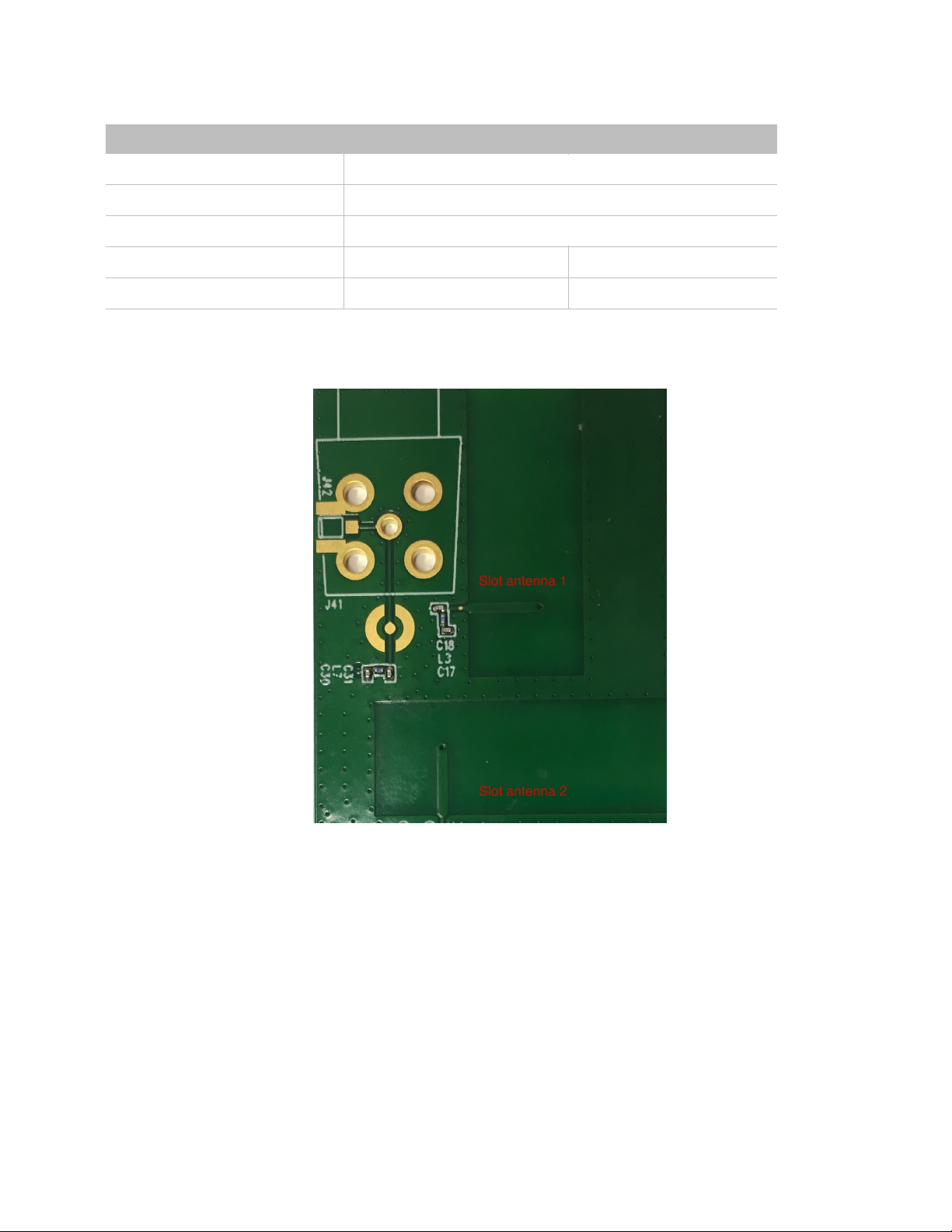
Table 1-2. Specifications of Slot Antennas
Description Slot antenna 1 Slot antenna 2
Storage temperature range –40 °C ~ +150 °C
Operating temperature range –40 °C ~ +85 °C
Frequency range 2.4 GHz ~ 2.5 GHz
Peak gain 3.56 dBi 4.20 dBi
Total efficiency 71.91% 87.43%
Figure 1-1 shows the two slot antennas.
Espressif Systems
2/!11
!
2018.10
Page 6

!
1. Overview
Espressif Systems
2018.10
The IPEX/U.FL antenna supported on the W11261889 has the following specifications
listed in Table 1-2:
Table 1-2. Specifications of IPEX/U.FL Antenna
Description Specifications
Cable length 100 mm
Storage temperature range –40 °C ~ +95 °C
Operating temperature range –30 °C ~ +85 °C
Frequency range 2.4 GHz ~ 2.5 GHz
Peak gain 3.0 dBi
Total efficiency >75%
Return loss <–10 dB
Polarization Linear
Input impedance 50 Ohms
The figure below shows the IPEX/U.FL antenna.
!
Figure 1-1. IPEX/U.FL Antenna (Top View)
!3/11
Page 7

!
2. Pin Description
2. Pin Description
2.1. Pin Layout
!
Figure 2-1. RIGEL REV C Pin Layout (Top View)
RIGEL REV C
1
2
3
4
5
6
7
8
9
10
11
12
13
14
15
VSS
VDD33
GPI36_WKUP_WIN
GPI39_WKUP_IN
GPIO15_WKUP_OUT_MTDO
GPIO14_MTMS
GPIO12_MTDI
GPIO13_MTCK
GPIO15_WKUP_OUT_MTDO
GPIO2_I2S_DA
GPIO0_I2S_CLK/Boot
GPIO4_I2S_SEL
GPI38_UART2_RX
GPIO26_UART2_TX
VSS
16
17
18
19
20
21
22
23
24
25
26
27
28
29
30
VSS
EN
UART0_TX
UART0_RX
GPIO0_I2S_CLK/Boot
GPI37_WIN_RX
GPIO27_WIN_TX
GPIO25_DP_RST
GPIO33_DP_CD
GPI34_DP_TE
GPIO5_DSP_CS
GPIO18_DP_CLK
GPIO23_DP_MOSI
GPIO19_DP_MISO
GPIO32_DP_CTRL
VDD33
VSS
VSS
VSS
NC1
NC2
NC3
NC4
NC5
VSS
31
32
33
34
35
36
37
38
39
40
Espressif Systems
2018.10
!4/11
Page 8

!
2. Pin Description
2.2. Pin List
RIGEL REV C has 40 pins. Please see the pin definitions in Table 2-1.
Table 2-1. RIGEL Pin Definitions
Solder No.
Pin No.
Pin Name
Type
Functional Description
J11VSS
Power
Ground
J22VDD33
Power
3.3 V input
J33GPI36_WKUP_WIN
GPIO
Interrupt input from WIN bus
J44GPI39_WKUP_IN
GPIO
Input from class B micro to SoC
J55GPIO15_WKUP_OUT_MTDO
GPIO
Output from SOC to class B micro
J66GPIO14_MTMS
JTAG
JTAG for debugging only
J77GPIO12_MTDI
JTAG
JTAG for debugging only
J88GPIO13_MTCK
JTAG
JTAG for debugging only
J99GPIO15_WKUP_OUT_MTDO
JTAG
JTAG for debugging only
J1010GPIO2_I2S_DA
I2S
I2S data to class D amplifier
J1111GPIO0_I2S_CLK/Boot
I2S
I2S clock to class D amplifier
J1212GPIO4_I2S_SEL
I2S
I2S select to class D amplifier
J1313GPI38_UART2_RX
UART
UART TX of class B to RX of SoC
J1414GPIO26_UART2_TX
UART
UART RX of class B to TX of SoC
J1515VSS
Power
Ground
J1616GPIO32_DP_CTRL
GPIO
PWM signal from SoC to back light for
dimming
J17
17
GPIO19_DP_MISO
SPI
SPI data out from display to SoC
J1818GPIO23_DP_MOSI
SPI
SPI data in to display from SoC
J1919GPIO18_DP_CLK
SPI
SPI CLK
J2020GPIO5_DSP_CS
SPI
SPI chip select
J2121GPI34_DP_TE
GPIO
Interrupt line input from display to SoC
J2222GPIO33_DP_CD
GPIO
SPI - command or data between SoC &
display
J2323GPIO25_DP_RST
GPIO
SPI- reset output from SoC to display
J2424GPIO27_WIN_TX
UART
UART RX of WIN host to TX to SoC
J2525GPI37_WIN_RX
UART
UART TX of WIN host to RX of SoC
Espressif Systems
2018.10
!5/11
Page 9

!
2. Pin Description
J2626GPIO0_I2S_CLK/Boot
GPIO
Boot / ESP32 only
J2727UART0_RX
UART
UART programming - RX ESP32
J2828UART0_TX
UART
UART programming - TX ESP32
J2929EN
GPIO
Enable / ESP32 only
J3030VSS
Power
Ground
J3131VDD33
Power
3.3 V input
J3232VSS
Power
Ground
J3333VSS
Power
Ground
J3434VSS
Power
Ground
J3535NC-Reserved
J3636NC-Reserved
J3737NC-Reserved
J3838NC-Reserved
J3939NC-Reserved
J4040VSS
Power
Ground
Solder No.
Pin No.
Pin Name
Type
Functional Description
Espressif Systems
2018.10
!6/11
Page 10

!
3. Peripherals and Interfaces
3. Peripherals and Interfaces
3.1. Radio/SOC & Class B Micro
UART should be used to interface between the Radio/SOC and the class B micro. The
Radio/SOC provides a wake-up input line (GPI39_WKUP_IN) and an interrupt output line
(GPIO15_WKUP_OUT_MTDO) to the class B micro.
3.2. Radio/SOC & WIN Bus
The Radio/SOC provides UART communication (GPIO27_WIN_TX/GPI37_WIN_RX) to the
WIN bus for optional use. Flow control is not required.
3.3. Interface—Display
The Radio/SOC provides eight signal lines (a 4-line SPI and 4 GPIOs) to display:
• Display reset
• SPI data out from display
•
SPI SS
• SPI CLK
• SPI data in to display
•
Display CD
• Display TE
• Display control for back-light driver
3.4. Interface—JATG
The Radio/SOC provides a JTAG interface for debugging. However, this interface should
only be used during the development.
3.5. Interface—Programming
The Radio/SOC provides a standalone programming interface, which includes
UART0_RX, UART0_TX, GPIO0_I2S_CLK/Boot, EN, VDD and GND.
Espressif Systems
2018.10
!7/11
Page 11

!
3. Peripherals and Interfaces
3.6. Interface—Audio
The Radio/SOC provides an I2S interface for driving the external digital audio.
Espressif Systems
2018.10
!8/11
Page 12

!
4. Electrical Characteristics
4. Electrical Characteristics
4.1. Absolute Maximum Ratings
Stresses beyond the absolute maximum ratings listed in the table below may cause
permanent damage to the device. These are stress ratings only, and do not refer to the
functional operation of the device.
4.2. Recommended Operating Conditions
4.3. DC Characteristics (3.3 V, 25 °C)
Table 4-1. Absolute Maximum Ratings
Symbol
Parameter
Min
Max
Unit
VDD33
-
–0.3
3.6
V
T
store
1
Storage temperature
–40
150
°C
⚠ Notice:
1. The storage temperature range for the module that uses IPEX/U.FL antenna is –40 °C ~ +95 °C.
Table 4-2. Recommended Operating Conditions
Symbol
Parameter
Min
Typ
Max
Unit
VDD33
-
2.7
3.3
3.6
V
I
VDD
Current delivered by
external power supply
0.5--
A
T 1Operating temperature
–40-85
°C
⚠ Notice:
1. The operating temperature range for the module that uses IPEX/U.FL antenna is –30 °C ~ +85 °C.
Table 4-3: DC Characteristics
Symbol
Parameter
Min
Typ
Max
Unit
CINPin capacitance
-2-
pF
VIHHigh-level input voltage
0.75×VDD
1
-
VDD1+0.3
V
Espressif Systems
2018.10
!9/11
Page 13

!
4. Electrical Characteristics
1. VDD is the I/O voltage for a particular power domain of pins. More details can be found
in Appendix IO_MUX of ESP32 Datasheet.
4.4. Wi-Fi Radio Characteristics
VIHHigh-level input voltage
0.75×VDD
1
-
VDD1+0.3
V
VILLow-level input voltage
–0.3-0.25×VDD
1
V
IIHHigh-level input current
--50
nA
IILLow-level input current
--50
nA
VOHHigh-level output voltage
0.8×VDD
1
--V
VOLLow-level output voltage
--0.1×VDD
1
V
I
OH
High-level source current (VDD1 = 3.3 V,
V
OH
>= 2.64 V, PAD_DRIVER = 3)
-40-
mA
I
OL
Low-level sink current (VDD1 = 3.3 V, V
OL
= 0.495 V, PAD_DRIVER = 3)
-28-
mA
RPUPull-up resistor
-45-
kΩ
RPDPull-down resistor
-45-
kΩ
V
IL_nRST
Low-level input voltage of EN to reset the
module
--0.6
V
Symbol
Parameter
Min
Typ
Max
Unit
Table 4-4. Wi-Fi Radio Characteristics
Parameter
Condition
Min
Typ
Max
Unit
Input frequency
-
2412
-
MHz
Output impedance*
--*-Ω
Espressif Systems
2018.10
2462
RF power
Sensitivity
20.09
-
21.21
dBm
11b, 1 Mbps - –98 - dBm
11b, 11 Mbps - –89 - dBm
11g, 6 Mbps - –92 - dBm
11g, 54 Mbps - –74 - dBm
11n, HT20, MCS0 - –91 - dBm
11n, HT20, MCS7 - –71 - dBm
11n, HT40, MCS0 - –89 - dBm
!10/11
Page 14

!
4. Electrical Characteristics
Parameter Condition Min Typ Max Unit
Espressif Systems
2018.10
11n, HT40, MCS7 - –69 - dBm
11g, 6 Mbps - 31 - dB
Adjacent channel
rejection
11g, 54 Mbps - 14 - dB
11n, HT20, MCS0 - 31 - dB
11n, HT20, MCS7 - 13 - dB
*For the module that uses an IPEX/U.FL antenna, the output impedance is 50 Ω.!
5.0 BLE Radio
5.0.1 Receiver
Table 8: Receiver Characteristics – BLE
Parameter Conditions Min Typ Max Unit
Sensitivity @30.8% PER - - –97 - dBm
Maximum received signal @30.8% PER - 0 - - dBm
Co-channel C/I - - +10 - dB
F = F0 + 1 MHz - –5 - dB
F = F0 – 1 MHz - –5 - dB
Adjacent channel selectivity C/I
Out-of-band blocking performance
Intermodulation - –36 - - dBm
F = F0 + 2 MHz - –25 - dB
F = F0 – 2 MHz - –35 - dB
F = F0 + 3 MHz - –25 - dB
F = F0 – 3 MHz - –45 - dB
30 MHz ~ 2000 MHz –10 - - dBm
2000 MHz ~ 2400 MHz –27 - - dBm
2500 MHz ~ 3000 MHz 27– - - dBm
3000 MHz ~ 12.5 GHz –10 - - dBm
5.0.2 Transmitter
Parameter Conditions Min Typ Max Unit
Gain control step
RF power control range - –
Adjacent channel transmit power
∆ f1
∆ f2
∆ f2
ICFT - - –10 - kHz
Drift rate - - 0.7 - kHz/50 µs
Drift - - 2 - kHz
avg
max
avg
/∆ f1
avg
Table 9: Transmitter Characteristics – BLE
-
F = F0 ± 2 MHz - 52– - dBm
F = F0 ± 3 MHz - –58 - dBm
F = F0 ± > 3 MHz - –60 - dBm
- - - 265 kHz
- 247 - - kHz
- - 0.92– - -
-
1.73
!10/11
3
-
-
-0.23
dBm
dBm
Page 15

!
6. Dimensions
5.
Dimensions
!
Figure 6-1. Dimensions of RIGEL REV C!
63
1.7
1
3.4
0.9
1.75x14=24.5
1.75
1.75x5=8.75
0.85
1.75x3=5.25
10.19
14.18
3.5
3.5
1.7
0.9
0.45
26.42
23.75
1.4
1.4
26.5
Note:1.Unit: mm
2.Unmarked tolerance: ±0.1 mm
1
15
31
16
40
30
Ø0.5
Espressif Systems
2018.10
!11/!11
Page 16

Disclaimer and Copyright Notice
Information in this document, including URL references, is subject to change without
notice.
THIS DOCUMENT IS PROVIDED AS IS WITH NO WARRANTIES WHATSOEVER,
INCLUDING ANY WARRANTY OF MERCHANTABILITY, NON-INFRINGEMENT, FITNESS
FOR ANY PARTICULAR PURPOSE, OR ANY WARRANTY OTHERWISE ARISING OUT
OF ANY PROPOSAL, SPECIFICATION OR SAMPLE.
All liability, including liability for infringement of any proprietary rights, relating to use of
information in this document is disclaimed. No licenses express or implied, by estoppel or
otherwise, to any intellectual property rights are granted herein.
The Wi-Fi Alliance Member logo is a trademark of the Wi-Fi Alliance. The Bluetooth logo is
a registered trademark of Bluetooth SIG.
All trade names, trademarks and registered trademarks mentioned in this document are
property of their respective owners, and are hereby acknowledged.
Copyright © 2018 Espressif Inc. All rights reserved.
Espressif IoT Team"
www.espressif.com
FCC Statement
Any Changes or modifications not expressly approved by the party responsible for
compliance could void the user’s authority to operate the equipment.
This device complies with part 15 of the FCC Rules. Operation is subject to the
following two conditions: (1) This device may not cause harmful interference, and (2)
This device must accept any interference received, including interference that may
cause undesired operation.
FCC Radiation Exposure Statement:
This equipment complies with FCC radiation exposure limits set forth for an
uncontrolled environment .This equipment should be installed and operated with
minimum distance 20cm between the radiator& your body.
FCC Label Instructions
The outside of final products that contains this module device must display a label
referring to the enclosed module. This exterior label can use wording such as:
“Contains Transmitter Module FCC ID:2AC7Z-RIGEL" or “Contains
FCC ID:2AC7Z-RIGEL” Any similar wording that expresses the same meaning may
be used.
Note: This equipment has been tested and found to comply with the limits for a Class
B digital device, pursuant to part 15 of the FCC Rules. These limits are designed to
provide reasonable protection against harmful interference in a residential installation.
This equipment generates, uses and can radiate radio frequency energy and, if not
installed and used in accordance with the instructions, may cause harmful
interference to radio communications. However, there is no guarantee that
interference will not occur in a particular installation. If this equipment does cause
harmful interference to radio or television reception, which can be determined by
turning the equipment off and on, the user is encouraged to try to correct the
interference by one or more of the following measures:
—Reorient or relocate the receiving antenna.
—Increase the separation between the equipment and receiver.
—Connect the equipment into an outlet on a circuit different from that to which the
receiver is connected.
—Consult the dealer or an experienced radio/TV technician for help.
 Loading...