

Page 1

ESP32-WROOM-32DC
Datasheet
Prerelease version 0.1
Espressif Systems
Copyright © 2018
CONFIDENTIAL
www.espressif.com
Page 2

About This Document
This document provides the specifications for the ESP32-WROOM-32DC module.
Revision History
For revision history of this document, please refer to the last page.
Documentation Change Notification
Espressif provides email notifications to keep customers updated on changes to technical documentation.
Please subscribe at www.espressif.com/en/subscribe.
Certification
Download certificates for Espressif products from www.espressif.com/en/certificates.
Disclaimer and Copyright Notice
Information in this document, including URL references, is subject to change without notice. THIS DOCUMENT
IS PROVIDED AS IS WITH NO WARRANTIES WHATSOEVER, INCLUDING ANY WARRANTY OF
MERCHANTABILITY, NON-INFRINGEMENT, FITNESS FOR ANY PARTICULAR PURPOSE, OR ANY WARRANTY
OTHERWISE ARISING OUT OF ANY PROPOSAL, SPECIFICATION OR SAMPLE.
All liability, including liability for infringement of any proprietary rights, relating to use of information in this
document is disclaimed. No licenses express or implied, by estoppel or otherwise, to any intellectual property
rights are granted herein. The Wi-Fi Alliance Member logo is a trademark of the Wi-Fi Alliance. The Bluetooth
logo is a registered trademark of Bluetooth SIG.
All trade names, trademarks and registered trademarks mentioned in this document are property of their
respective owners, and are hereby acknowledged.
Copyright © 2018 Espressif Inc. All rights reserved.
CONFIDENTIAL
Page 3

Contents
1 Overview 1
2 Pin Definitions 3
2.1 Pin Layout 3
2.2 Pin Description 3
2.3 Strapping Pins 4
3 Functional Description 6
3.1 CPU and Internal Memory 6
3.2 External Flash and SRAM 6
3.3 Crystal Oscillators 6
3.4 RTC and Low-Power Management 7
4 Peripherals and Sensors 8
5 Electrical Characteristics
5.1 Absolute Maximum Ratings
5.2 Recommended Operating Conditions
5.3 DC Characteristics (3.3 V, 25 °C)
5.4 Reflow Profile
6 Physical Dimensions
7 Recommended PCB Land Pattern
8 Learning Resources
8.1 Must-Read Documents
8.2 Must-Have Resources
Revision History
11
12
13
14
14
1
9
9
9
9
14
5
Page 4

List of Tables
1 ESP32-WROOM-32DC Specifications
2 Pin Definitions
3 Strapping Pins
4 Absolute Maximum Ratings
5 Recommended Operating Conditions
6 DC Characteristics (3.3 V, 25 °C)
1
3
5
9
9
9
CONFIDENTIAL
Page 5

List of Figures
1 ESP32-WROOM-32DC Pin Layout (Top View)
2 Reflow Profile
3 Physical Dimensions of ESP32-WROOM-32DC
4 Recommended PCB Land Pattern
3
11
12
13
CONFIDENTIAL
Page 6
1. Overview
1. Overview
ESP32-WROOM-32DC is a powerful, generic Wi-Fi+BT+BLE MCU module that targets a wide variety of
applications, ranging from low-power sensor networks to the most demanding tasks, such as voice encoding,
music streaming and MP3 decoding.
At the core of this module is the ESP32-D0WD chip*. The chip embedded is designed to be scalable and
adaptive. There are two CPU cores that can be individually controlled, and the CPU clock frequency is adjustable
from 80 MHz to 240 MHz. The user may also power off the CPU and make use of the low-power co-processor
to constantly monitor the peripherals for changes or crossing of thresholds. ESP32 integrates a rich set of
peripherals, ranging from capacitive touch sensors, Hall sensors, SD card interface, Ethernet, high-speed SPI,
UART, I2S and I2C.
Note:
* For details on the part numbers of the ESP32 family of chips, please refer to the document ESP32 Datasheet.
The integration of Bluetooth, Bluetooth LE and Wi-Fi ensures that a wide range of applications can be targeted,
and that the module is all-around: using Wi-Fi allows a large physical range and direct connection to the internet
through a Wi-Fi router, while using Bluetooth allows the user to conveniently connect to the phone or broadcast
low energy beacons for its detection. The sleep current of the ESP32 chip is less than 5 µA, making it suitable for
battery powered and wearable electronics applications. The module supports a data rate of up to 150 Mbps,
and 20 dBm output power at the antenna to ensure the widest physical range. As such the module does offer
industry-leading specifications and the best performance for electronic integration, range, power consumption,
and connectivity.
The operating system chosen for ESP32 is freeRTOS with LwIP; TLS 1.2 with hardware acceleration is built in as
well. Secure (encrypted) over the air (OTA) upgrade is also supported, so that developers can upgrade their
products even after their release, at minimum cost and effort.
Table 1 provides the specifications of ESP32-WROOM-32DC.
Table 1: ESP32-WROOM-32DC Specifications
Categories Items Specifications
802.11 b/g/n (802.11n up to 150 Mbps)
Wi-Fi
Bluetooth
Protocols
Frequency range 2.4 GHz ~ 2.5 GHz
Protocols Bluetooth v4.2 BR/EDR and BLE specification
Radio
CONFIDENTIAL
Audio CVSD and SBC
Hardware Module interface
On-chip sensor Hall sensor
On-board clock 40 MHz crystal
A-MPDU and A-MSDU aggregation and 0.4 µs guard
interval support
NZIF receiver with –97 dBm sensitivity
AFH
SD card, UART, SPI, SDIO, I2C, LED PWM, Motor
PWM, I2S, IR, pulse counter, GPIO, capacitive touch
sensor, ADC, DAC
Espressif Systems 1 ESP32-WROOM-32DC Datasheet V0.1
Page 7

1. Overview
Categories Items Specifications
Operating voltage/Power supply 2.7 V ~ 3.6 V
Operating current Average: 80 mA
Minimum current delivered by
power supply
Recommended operating tem-
perature range
Package size (mm) (18.00±0.10) × (25.50±0.10) × (3.10±0.10)
500 mA
–40 °C ~ +85 °C
CONFIDENTIAL
Espressif Systems 2 ESP32-WROOM-32DC Datasheet V0.1
Page 8

2. Pin Definitions
Keepout Zone
GND
IO23
IO22
TXD0
RXD0
IO21
NC
IO19
IO18
IO5
IO17
IO16
IO4
IO0
38
37
36
35
34
33
32
31
30
29
28
27
26
25
24
23
22
21
20
19
18
17
16
15
IO2
IO15
SD1
SD0
CLK
CMD
SD3
SD2
IO13
GND
1
2
3
4
5
6
7
8
9
10
11
12
13
14
GND
3V3
EN
SENSOR_VP
SENSOR_VN
IO34
IO35
IO32
IO33
IO25
IO26
IO27
IO14
IO12
39 GND
2. Pin Definitions
2.1 Pin Layout
Figure 1: ESP32-WROOM-32DC Pin Layout (Top View)
2.2 Pin Description
ESP32-WROOM-32DC has 38 pins. See pin definitions in Table 2.
Table 2: Pin Definitions
Name No. Type Function
GND 1 P Ground
3V3 2 P Power supply
EN 3 I Module-enable signal. Active high.
SENSOR_VP 4 I GPIO36, ADC1_CH0, RTC_GPIO0
CONFIDENTIAL
SENSOR_VN 5 I GPIO39, ADC1_CH3, RTC_GPIO3
IO34 6 I GPIO34, ADC1_CH6, RTC_GPIO4
IO35 7 I GPIO35, ADC1_CH7, RTC_GPIO5
IO32 8 I/O
IO33 9 I/O
GPIO32, XTAL_32K_P (32.768 kHz crystal oscillator input), ADC1_CH4,
TOUCH9, RTC_GPIO9
GPIO33, XTAL_32K_N (32.768 kHz crystal oscillator output), ADC1_CH5,
TOUCH8, RTC_GPIO8
Espressif Systems 3 ESP32-WROOM-32DC Datasheet V0.1
Page 9

2. Pin Definitions
Name No. Type Function
IO25 10 I/O GPIO25, DAC_1, ADC2_CH8, RTC_GPIO6, EMAC_RXD0
IO26 11 I/O GPIO26, DAC_2, ADC2_CH9, RTC_GPIO7, EMAC_RXD1
IO27 12 I/O GPIO27, ADC2_CH7, TOUCH7, RTC_GPIO17, EMAC_RX_DV
IO14 13 I/O
IO12 14 I/O
GND 15 P Ground
IO13 16 I/O
SHD/SD2* 17 I/O GPIO9, SD_DATA2, SPIHD, HS1_DATA2, U1RXD
SWP/SD3* 18 I/O GPIO10, SD_DATA3, SPIWP, HS1_DATA3, U1TXD
SCS/CMD* 19 I/O GPIO11, SD_CMD, SPICS0, HS1_CMD, U1RTS
SCK/CLK* 20 I/O GPIO6, SD_CLK, SPICLK, HS1_CLK, U1CTS
SDO/SD0* 21 I/O GPIO7, SD_DATA0, SPIQ, HS1_DATA0, U2RTS
SDI/SD1* 22 I/O GPIO8, SD_DATA1, SPID, HS1_DATA1, U2CTS
IO15 23 I/O
IO2 24 I/O
IO0 25 I/O GPIO0, ADC2_CH1, TOUCH1, RTC_GPIO11, CLK_OUT1, EMAC_TX_CLK
IO4 26 I/O
IO16 27 I/O GPIO16, HS1_DATA4, U2RXD, EMAC_CLK_OUT
IO17 28 I/O GPIO17, HS1_DATA5, U2TXD, EMAC_CLK_OUT_180
IO5 29 I/O GPIO5, VSPICS0, HS1_DATA6, EMAC_RX_CLK
IO18 30 I/O GPIO18, VSPICLK, HS1_DATA7
IO19 31 I/O GPIO19, VSPIQ, U0CTS, EMAC_TXD0
NC 32 - -
IO21 33 I/O GPIO21, VSPIHD, EMAC_TX_EN
RXD0 34 I/O GPIO3, U0RXD, CLK_OUT2
TXD0 35 I/O GPIO1, U0TXD, CLK_OUT3, EMAC_RXD2
IO22 36 I/O GPIO22, VSPIWP, U0RTS, EMAC_TXD1
IO23 37 I/O GPIO23, VSPID, HS1_STROBE
GND 38 P Ground
GPIO14, ADC2_CH6, TOUCH6, RTC_GPIO16, MTMS, HSPICLK, HS2_CLK,
SD_CLK, EMAC_TXD2
GPIO12, ADC2_CH5, TOUCH5, RTC_GPIO15, MTDI, HSPIQ, HS2_DATA2,
SD_DATA2, EMAC_TXD3
GPIO13, ADC2_CH4, TOUCH4, RTC_GPIO14, MTCK, HSPID, HS2_DATA3,
SD_DATA3, EMAC_RX_ER
GPIO15, ADC2_CH3, TOUCH3, MTDO, HSPICS0, RTC_GPIO13, HS2_CMD,
SD_CMD, EMAC_RXD3
GPIO2, ADC2_CH2, TOUCH2, RTC_GPIO12, HSPIWP, HS2_DATA0,
SD_DATA0
GPIO4, ADC2_CH0, TOUCH0, RTC_GPIO10, HSPIHD, HS2_DATA1,
SD_DATA1, EMAC_TX_ER
Notice:
CONFIDENTIAL
* Pins SCK/CLK, SDO/SD0, SDI/SD1, SHD/SD2, SWP/SD3 and SCS/CMD, namely, GPIO6 to GPIO11 are connected
to the integrated SPI flash integrated on the module and are not recommended for other uses.
2.3 Strapping Pins
ESP32 has five strapping pins, which can be seen in Chapter 6 Schematics:
Espressif Systems 4 ESP32-WROOM-32DC Datasheet V0.1
Page 10
2. Pin Definitions
• MTDI
• GPIO0
• GPIO2
• MTDO
• GPIO5
Software can read the values of these five bits from register ”GPIO_STRAPPING”.
During the chip’s system reset (power-on-reset, RTC watchdog reset and brownout reset), the latches of the
strapping pins sample the voltage level as strapping bits of ”0” or ”1”, and hold these bits until the chip is
powered down or shut down. The strapping bits configure the device’s boot mode, the operating voltage of
VDD_SDIO and other initial system settings.
Each strapping pin is connected to its internal pull-up/pull-down during the chip reset. Consequently, if a
strapping pin is unconnected or the connected external circuit is high-impedance, the internal weak
pull-up/pull-down will determine the default input level of the strapping pins.
To change the strapping bit values, users can apply the external pull-down/pull-up resistances, or use the host
MCU’s GPIOs to control the voltage level of these pins when powering on ESP32.
After reset, the strapping pins work as normal-function pins.
Refer to Table 3 for a detailed boot-mode configuration by strapping pins.
Table 3: Strapping Pins
Voltage of Internal LDO (VDD_SDIO)
Pin Default 3.3 V 1.8 V
MTDI Pull-down 0 1
Booting Mode
Pin Default SPI Boot Download Boot
GPIO0 Pull-up 1 0
GPIO2 Pull-down Don’t-care 0
Enabling/Disabling Debugging Log Print over U0TXD During Booting
Pin Default U0TXD Active U0TXD Silent
MTDO Pull-up 1 0
Timing of SDIO Slave
Pin Default
MTDO Pull-up 0 0 1 1
GPIO5 Pull-up 0 1 0 1
Falling-edge Input
Falling-edge Output
Falling-edge Input
Rising-edge Output
Rising-edge Input
Falling-edge Output
Rising-edge Input
Rising-edge Output
Note:
CONFIDENTIAL
• Firmware can configure register bits to change the settings of ”Voltage of Internal LDO (VDD_SDIO)” and ”Timing
of SDIO Slave” after booting.
• The module integrates a 3.3 V SPI flash, so the pin MTDI cannot be set to 1 when the module is powered up.
Espressif Systems 5 ESP32-WROOM-32DC Datasheet V0.1
Page 11

3. Functional Description
3. Functional Description
This chapter describes the modules and functions integrated in ESP32-WROOM-32DC.
3.1 CPU and Internal Memory
ESP32-D0WD contains two low-power Xtensa®32-bit LX6 microprocessors. The internal memory
includes:
• 448 KB of ROM for booting and core functions.
• 520 KB of on-chip SRAM for data and instructions.
• 8 KB of SRAM in RTC, which is called RTC FAST Memory and can be used for data storage; it is accessed
by the main CPU during RTC Boot from the Deep-sleep mode.
• 8 KB of SRAM in RTC, which is called RTC SLOW Memory and can be accessed by the co-processor
during the Deep-sleep mode.
• 1 Kbit of eFuse: 256 bits are used for the system (MAC address and chip configuration) and the remaining
768 bits are reserved for customer applications, including flash-encryption and chip-ID.
3.2 External Flash and SRAM
ESP32 supports multiple external QSPI flash and SRAM chips. More details can be found in Chapter SPI in
the
ESP32 Technical Reference Manual. ESP32 also supports hardware encryption/decryption based on AES to
protect developers’ programs and data in flash.
ESP32 can access the external QSPI flash and SRAM through high-speed caches.
• The external flash can be mapped into CPU instruction memory space and read-only memory space
simultaneously.
– When external flash is mapped into CPU instruction memory space, up to 11 MB + 248 KB can be
mapped at a time. Note that if more than 3 MB + 248 KB are mapped, cache performance will be
reduced due to speculative reads by the CPU.
– When external flash is mapped into read-only data memory space, up to 4 MB can be mapped at a
time. 8-bit, 16-bit and 32-bit reads are supported.
• External SRAM can be mapped into CPU data memory space. Up to 4 MB can be mapped at a time.
8-bit, 16-bit and 32-bit reads and writes are supported.
ESP32-WROOM-32DC integrates 4 MB of external SPI flash. The 4-MB SPI flash can be memory-mapped onto
the CPU code space, supporting 8, 16 and 32-bit access. Code execution is supported. The integrated SPI
CONFIDENTIAL
flash is connected to GPIO6, GPIO7, GPIO8, GPIO9, GPIO10 and GPIO11. These six pins cannot be used as
regular GPIOs.
3.3 Crystal Oscillators
The module uses a 40-MHz crystal oscillator.
Espressif Systems 6 ESP32-WROOM-32DC Datasheet V0.1
Page 12

3. Functional Description
3.4 RTC and Low-Power Management
With the use of advanced power-management technologies, ESP32 can switch between different power
modes.
For details on ESP32’s power consumption in different power modes, please refer to section ”RTC and
Low-Power Management” in ESP32 Datasheet.
CONFIDENTIAL
Espressif Systems 7 ESP32-WROOM-32DC Datasheet V0.1
Page 13

4. Peripherals and Sensors
4. Peripherals and Sensors
Please refer to Section Peripherals and Sensors in ESP32 Datasheet.
Note:
External connections can be made to any GPIO except for GPIOs in the range 6-11. These six GPIOs are connected to
the module’s integrated SPI flash. For details, please see Section 6 Schematics.
CONFIDENTIAL
Espressif Systems 8 ESP32-WROOM-32DC Datasheet V0.1
Page 14

5. Electrical Characteristics
5. Electrical Characteristics
5.1 Absolute Maximum Ratings
Stresses beyond the absolute maximum ratings listed in the table below may cause permanent damage to the
device. These are stress ratings only, and do not refer to the functional operation of the device.
Table 4: Absolute Maximum Ratings
Symbol Parameter Min Max Unit
VDD33 Power supply voltage –0.3 3.6 V
T
store
1
I
O
1. The module worked properly after a 24-hour test in ambient temperature at 25 °C, and the IOs in three domains
(VDD3P3_RTC, VDD3P3_CPU, VDD_SDIO) output high logic level to ground. Please note that pins occupied by flash
and/or PSRAM in the VDD_SDIO power domain were excluded from the test.
2. Please see Appendix IO_MUX of ESP32 Datasheet for IO’s power domain.
Storage temperature –40 150 °C
Cumulative IO output current - 1,100 mA
5.2 Recommended Operating Conditions
Table 5: Recommended Operating Conditions
Symbol Parameter Min Typical Max Unit
VDD33 Power supply voltage 2.7 3.3 3.6 V
I
V DD
T Operating temperature –40 - 85 °C
Current delivered by external power supply 0.5 - - A
5.3 DC Characteristics (3.3 V, 25 °C)
Table 6: DC Characteristics (3.3 V, 25 °C)
Symbol Parameter Min Typ Max Unit
C
IN
V
IH
V
IL
I
IH
I
IL
V
OH
V
OL
CONFIDENTIAL
High-level source current VDD3P3_CPU power domain
I
OH
I
OL
R
P U
(VDD1= 3.3 V, VOH>= 2.64 V, VDD3P3_RTC power domain
PAD_DRIVER = 3) VDD_SDIO power domain
Low-level sink current
(VDD1= 3.3 V, VOL= 0.495 V, PAD_DRIVER = 3)
Pin capacitance - 2 - pF
High-level input voltage 0.75×VDD1- VDD1+0.3 V
Low-level input voltage –0.3 - 0.25×VDD1V
High-level input current - - 50 nA
Low-level input current - - 50 nA
High-level output voltage 0.8×VDD1- - V
Low-level output voltage - - 0.1×VDD1V
1, 2
- 40 - mA
1, 2
- 40 - mA
1, 3
Pull-up resistor - 45 - kΩ
- 20 - mA
- 28 - mA
Espressif Systems 9 ESP32-WROOM-32DC Datasheet V0.1
Page 15

5. Electrical Characteristics
Symbol Parameter Min Typ Max Unit
R
P D
V
IL_nRS T
Notes:
1. Please see Appendix IO_MUX of ESP32 Datasheet for IO’s power domain. VDD is the I/O voltage for a particular power
domain of pins.
2. For VDD3P3_CPU and VDD3P3_RTC power domain, per-pin current sourced in the same domain is gradually reduced
from around 40 mA to around 29 mA, VOH>=2.64 V, as the number of current-source pins increases.
3. Pins occupied by flash and/or PSRAM in the VDD_SDIO power domain were excluded from the test.
Low-level input voltage of CHIP_PU to reset the chip - - 0.6 V
Pull-down resistor - 45 - kΩ
Espressif Systems 10 ESP32-WROOM-32DC Datasheet V0.1
Page 16

5. Electrical Characteristics
50
150
0
25
1 ~ 3℃/s
0
200
250
200
-1 ~ -5℃/s
Cooling zone
100
217
50
100 250
Reflow zone
!217℃ 60 ~ 90s
Temperature (℃)
Preheating zone
150 ~ 200℃ 60 ~ 120s
Ramp-up zone
Peak Temp.
235 ~ 250℃
Soldering time
> 30s
Time (sec.)
Ramp-up zone — Temp.: <150℃ Time: 60 ~ 90s Ramp-up rate: 1 ~ 3℃/s
Preheating zone — Temp.: 150 ~ 200℃ Time: 60 ~ 120s Ramp-up rate: 0.3 ~ 0.8℃/s
Reflow zone — Temp.: >217℃ 7LPH60 ~ 90s; Peak Temp.: 235 ~ 250℃ (<245℃ recommended) Time: 30 ~ 70s
Cooling zone — Peak Temp. ~ 180℃ Ramp-down rate: -1 ~ -5℃/s
Solder — Sn&Ag&Cu Lead-free solder (SAC305)
5.4 Reflow Profile
CONFIDENTIAL
Figure 2: Reflow Profile
Espressif Systems 11 ESP32-WROOM-32DC Datasheet V0.1
Page 17

PCB Thickness
Module Thickness
3.10±0.10
0.80±0.10
1.27±0.10
1.50±0.10
17.60±0.10
Module Width
Module Length
1.27±0.10
11.43±0.10
25.50±0.10
18.00±0.10
Unit: mm
16.51±0.10
11.43±0.10
3.28±0.10
1.27±0.10
25.50±0.10
ESP32-WROOM-32DC DIMENSIONS
Top View
Side View
Bottom View
Antenna Area
0.90±0.10
0.85±0.10
6.20±0.10
15.80±0.10
1.50±0.10
0.45±0.10
0.90±0.10
18.00±0.10
3.28±0.10
∅0.50±0.10
6.40±0.10
9.20±0.10
2.20±0.10
2.20±0.10
Espressif Systems 12 ESP32-WROOM-32DC Datasheet V0.1
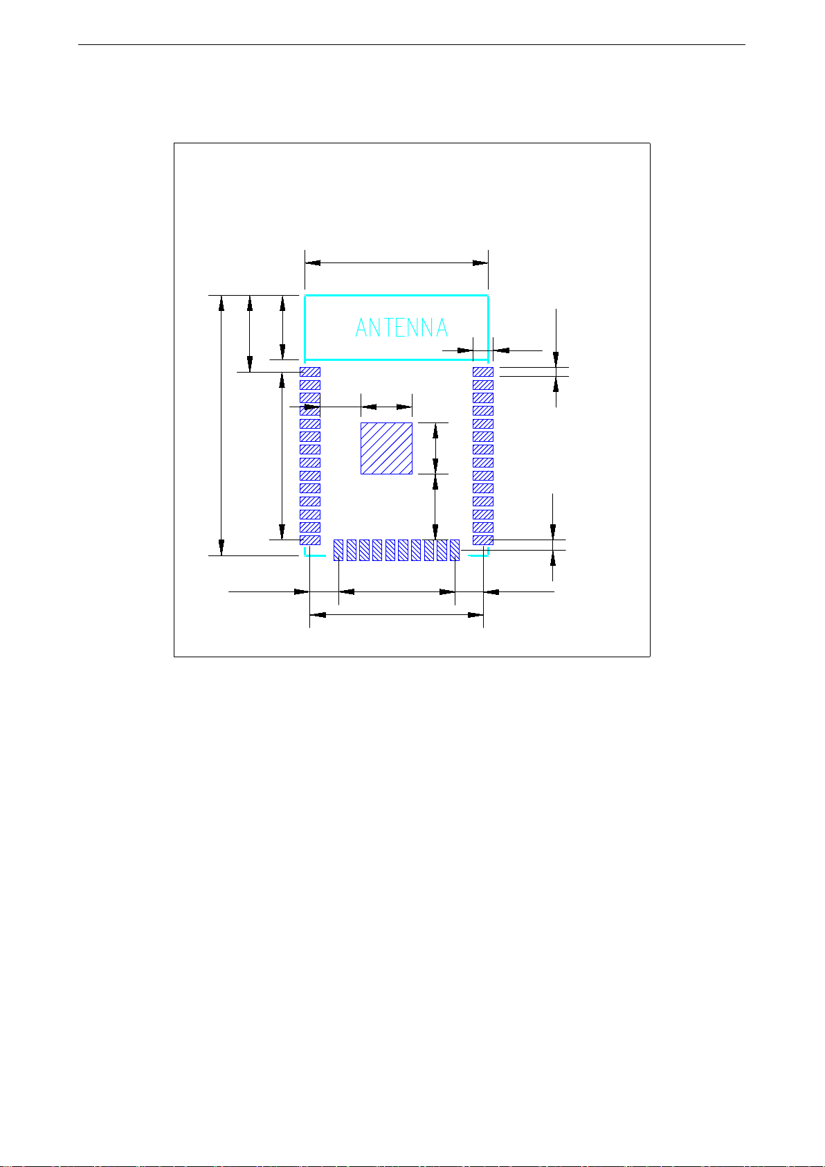
6.
Physical Dimensions
CONFIDENTIAL
6
Physical Dimensions
Figure 3: Physical Dimensions of ESP32-WROOM-32DC
Page 18
Recommended PCB Land Pattern
25.5
18
1.27x13=16.51
1.27x9=11.432.785
1
2
6.3
17
7.49
2.785
5
5
0.9
1
15 24
38
Unit:mm
6.51
4
7.
7.
Recommended PCB Land Pattern
Figure4: Recommended PCB Land Pattern
CONFIDENTIAL
Espressif Systems 13 ESP32-WROOM-32DC Datasheet V0.1
Page 19

8
Learning Resources
8.
Learning Resources
8.1 Must-Read Documents
The following link provides documents related to ESP32.
• ESP32 Datasheet
This document provides an introduction to the specifications of the ESP32 hardware, including overview,
pin definitions, functional description, peripheral interface, electrical characteristics, etc.
• ESP-IDF Programming Guide
It hosts extensive documentation for ESP-IDF ranging from hardware guides to API reference.
• ESP32 Technical Reference Manual
The manual provides detailed information on how to use the ESP32 memory and peripherals.
• ESP32 Hardware Resources
The zip files include the schematics, PCB layout, Gerber and BOM list of ESP32 modules and development
boards.
• ESP32 Hardware Design Guidelines
The guidelines outline recommended design practices when developing standalone or add-on systems
based on the ESP32 series of products, including the ESP32 chip, the ESP32 modules and development
boards.
• ESP32 AT Instruction Set and Examples
This document introduces the ESP32 AT commands, explains how to use them, and provides examples of
several common AT commands.
• Espressif Products Ordering Information
8.2 Must-Have Resources Here
are the ESP32-related must-have resources.
• ESP32 BBS
This is an Engineer-to-Engineer (E2E) Community for ESP32 where you can post questions, share
knowledge, explore ideas, and help solve problems with fellow engineers.
• ESP32 GitHub
ESP32 development projects are freely distributed under Espressif’s MIT license on GitHub. It is
established to help developers get started with ESP32 and foster innovation and the growth of general
knowledge about the hardware and software surrounding ESP32 devices.
• ESP32 Tools
This is a webpage where users can download ESP32 Flash Download Tools and the zip file ”ESP32
CONFIDENTIAL
Certification and Test”.
• ESP-IDF
This webpage links users to the official IoT development framework for ESP32.
• ESP32 Resources
This webpage provides the links to all available ESP32 documents, SDK and tools. �����������
Espressif Systems 14 ESP32-WROOM-32DC Datasheet V0.1
Page 20

Revision History
Revision History
Date Version Release notes
2018.10 V0.1 Preliminary release.
FCC Statement
Any Changes or modifications not expressly approved by the party
responsible for compliance could void the user’s authority to operate
the equipment.
This device complies with part 15 of the FCC Rules. Operation is
subject to the following two conditions:
(1) This device may not cause harmful interference, and
(2) This device must accept any interference received, including
interference that may cause undesired operation.
FCC Radiation Exposure Statement:
This equipment complies with FCC radiation exposure limits set forth
for an uncontrolled environment .This equipment should be installed
and operated with minimum distance 20cm between the radiator&
your body.
FCC Label Instructions:
The outside of final products that contains this module device must
display a label referring to the enclosed module. This exterior label
can use wording such as: “Contains Transmitter Module
FCC ID: 2AC7Z-ESPWROOM32DC”,or “Contains
FCC ID: 2AC7Z-ESPWROOM32DC”, Any similar wording that
expresses the same meaning may be used.
CONFIDENTIAL
Espressif Systems 15 ESP32-WROOM-32DC Datasheet V0.1
 Loading...