

Page 1

ESP8089M16
Datasheet
Version 1.0
Copyright © 2017
Page 2

This document provides introduction to the specifications of ESP8089M16 module.
Release Notes
Date Version Release notes
2017.07 V1.0 First release.
Documentation Change Notification
Espressif provides email notifications to keep customers updated on changes to
technical documentation. Please subscribe here.
About This Guide
Page 3

Table of Contents
1. Overview 1 ................................................................................................................................
1.1. Features! 1"....................................................................................................................................
1.2. Applications! 1"..............................................................................................................................
2. Pin Assignments 2 ....................................................................................................................
2.1. PCB Pin Outline! 2"........................................................................................................................
2.2. Pin Definition! 2"............................................................................................................................
3. Functional Description 4 ..........................................................................................................
3.1. Block Diagram! 4"..........................................................................................................................
3.2. External Clock Reference! 4".........................................................................................................
4. Peripheral Interface 5 ..............................................................................................................
4.1. SDIO Pin Description! 5"...............................................................................................................
4.2. SDIO Default Mode Timing Diagram! 6"........................................................................................
5. Electrical Characteristics 7 ......................................................................................................
5.1. Absolute Maximum Ratings! 7".....................................................................................................
5.2. Operating Conditions! 7"...............................................................................................................
5.3. RF Characteristics for IEEE802.11b/g/n! 7"..................................................................................
6. Module Dimensions 10 .............................................................................................................
6.1. Top View and Side View! 10".........................................................................................................
6.2. Recommended Footprint! 11".......................................................................................................
7. Packing Information 12............................................................................................................
Page 4

1. Overview
!
1. Overview
ESP8089M16 is the small-sized low-power module for IEEE 802.11b/g/n wireless LAN.
ESP8089M16 is based on the ESP8089 solution. (More information on ESP8089 can be
found in the ESP8089 Datasheet.)
ESP8089M16 features a small size of 12.0 (± 0.1) x 12.0 (± 0.1) x 1.5 (± 0.1) mm, making it
an ideal choice for space-constrained applications.
1.1. Features
•
IEEE 802.11 b/g/n single ANT WLAN infrastructure
•
Wi-Fi Direct (P2P)
•
Built-in TCP/IP protocol stack
•
Built-in TR switch, balun, LAN power amplifier and matching network
•
Built-in PLL voltage regulator and power management module
•
Power-off leakage current is less than 4 μA
•
Built-in low-power 32-bit CPU: can be used as an application processor
•
SDIO 11, SPI, UART
•
Collaborated 22 ms wake-up ,within the connection and transmission of data
packets
•
Standby power consumption is less than 1.0 mW (DTIM3)
•
2.4 GHz internal PA
1.2. Applications
•
Digital Television (DTV)
•
Digital Video Recorder (DVR)
•
HD DVD Player
•
Blue-ray Disk Player
•
Set Top Box (STB)
•
Mobile Internet Device (MID)
•
Over The Top (OTT)!
Espressif ! /!1 13
2017.07
Page 5

2. Pin Assignments
!
2. Pin Assignments
2.1. PCB Pin Outline
2.2. Pin Definition
No. Pin Name Type Description
1 GND - Ground connection
2 WL_BT_ANT I/O RF I/O port
3 GND - Ground connection
4 NC - Floating (Don't connect to ground)
5 NC - Floating (Don't connect to ground)
6 NC - Floating (Don't connect to ground)
7 NC - Floating (Don't connect to ground)
8 NC - Floating (Don't connect to ground)
9 VBAT P Main power voltage source input
10 XTAL_IN I XTAL oscillator input
11 XTAL_OUT O XTAL oscillator output
!
Table 2-1. Pin Definition
Espressif ! /!2 13
2017.07
Page 6

2. Pin Assignments
!
No. Pin Name Type Description
12 WL_REG_ON I WIFI_EN
13 WL_HOST_WAKE O WLAN_INT
14 SDIO_DATA_2 I/O SDIO data line 2
15 SDIO_DATA_3 I/O SDIO data line 3
16 SDIO_DATA_CMD I/O SDIO command line
17 SDIO_DATA_CLK I/O SDIO CLK line
18 SDIO_DATA_0 I/O SDIO data line 0
19 SDIO_DATA_1 I/O SDIO data line 1
20 GND - Ground connection
21 VIN_LDO_OUT P NC
22 VDDIO P I/O voltage supply input
23 VIN_LDO P Internal buck voltage generation pin
24 LPO I External low-power clock input (32.768 KHz)
25 NC - Floating (Don't connect to ground)
26 NC - Floating (Don't connect to ground)
27 NC - Floating (Don't connect to ground)
28 NC - Floating (Don't connect to ground)
29 NC - Floating (Don't connect to ground)
30 NC - Floating (Don't connect to ground)
31 GND - Ground connection
32 NC - Floating (Don't connect to ground)
33 GND - Ground connection
34 NC - Floating (Don't connect to ground)
35 NC - Floating (Don't connect to ground)
36 GND - Ground connection
37 NC - Floating (Don't connect to ground)
38 NC - Floating (Don't connect to ground)
39 NC - Floating (Don't connect to ground)
40 NC - Floating (Don't connect to ground)
41 NC - Floating (Don't connect to ground)
42 NC - Floating (Don't connect to ground)
43 NC - Floating (Don't connect to ground)
44 NC - Floating (Don't connect to ground)
Espressif ! /!3 13
2017.07
Page 7

3. Functional Description
!
3. Functional Description
3.1. Block Diagram
RF
receive
Switch
RF
transmit
PLL 1/2
PMU Crystal
VCO
!
3.2. External Clock Reference
Table 3-1. External Clock Signal Characteristics
No. Item Symb.
Analog
receive
Analog
transmit
Digital Baseband
PLL
Bias circuits SRAM PMU
MAC Interface
Registers
SDIO
CPU
Sequencers
GPIO
Accelerator
Electrical specification
Remark
Min. Type Max. Unit
1 Nominal frequency F0 40 MHz -
2 Mode of vibration - Fundamental -
3 Frequency tolerance
4
Operating temperature
range
F/F0 -10 - 10 ppm At 25±3℃
Δ
T
OPR
5 Frequency stability TC -10 - 10 ppm -
6 Storage temperature T
STG
7 Load capacitance CL - 15 - pF -
8 Drive level DL - 100 200 μW -
9 Insulation resistance IR 500 - - MΩ At 100 V
10 Shunt capacitance C0 - - 7 pF -
11 Aging per year Fa -3 - 3 ppm First year
Espressif ! /!4 13
-40 - 85 ℃ -
-40 - 85 ℃ -
DC
2017.07
Page 8

4. Peripheral Interface
!
4. Peripheral Interface
4.1. SDIO Pin Description
The module supports SDIO version 2.0 for 4-bit mode. It has the ability to stop the SDIO
clock and map the interrupt signal into a GPIO pin. This ‘out-of-band’ interrupt signal
notifies the host when the WLAN device wants to turn on the SDIO interface. The ability to
force the control of the gated clocks from within the WLAN chip is also provided.
Function 0: Standard SDIO function (Max BlockSize/ByteCount = 32B)
•
•
Function 1: Backplane function to access the internal System-on-Chip (SoC) address
space (Max BlockSize/ByteCount = 64B)
•
Function 2: WLAN function for efficient WLAN packet transfer through DMA (Max
BlockSize/ByteCount=512B)
The SDIO 4-bit mode is shown as follows:
DATA0 Data line 0
DATA1 Data line 1 or interrupt
DATA2 Data line 2 or read wait
DATA3 Data line 3
CLK Clock
CMD Command line
Espressif ! /!5 13
2017.07
Page 9

!
4.2. SDIO Default Mode Timing Diagram
4. Peripheral Interface
!
Figure 4-1. SDIO Default Mode Timing Diagram
Table 4-1. SDIO Timing Characteristics
Parameter Symbol Min Max Unit
Input setup time t
Input hold time t
Clock falling time t
Clock rising time t
Output delay t
ISU
IH
THL
TLH
DLY
6 - ns
2.5 - ns
- 3 ns
- 3 ns
2 12 ns
Espressif ! /!6 13
2017.07
Page 10

5. Electrical Characteristics
!
5. Electrical Characteristics
5.1. Absolute Maximum Ratings
📖 Note:
The specifications in the table below define levels at which permanent damage to the device can occur.
Function operation is not guaranteed under these conditions. Operating at absolute maximum conditions for
extend periods can adversely affect the long-term reliability of the device.
Table 5-1. Absolute Maximum Ratings
Parameter Min Max Unit
Storage temperature -40 85 ℃
Storage humidity (40℃) - 90% %
•
Do not use or store modules in the corrosive atmosphere, especially where chloride gas,
sulfide gas, acid, alkali, salt or the like are contained. Also, avoid exposure to moisture.
•
Store the modules where the temperature and relative humidity do not exceed 5 to 40℃
and 20 to 60%.
•
Assemble the modules within six months. Check the soldering ability in case of over six
months.
5.2. Operating Conditions
Parameter Min Typ Max Unit
Operating temperature -40 - 85 ℃
Operating humidity - - 85 %
VBAT 2.7 3.3 3.6 V
VIO 1.8 2.8 - V
Table 5-2. Operating Conditions
5.3. RF Characteristics for IEEE802.11b/g/n
The test for electrical specification shall be performed under the following conditions unless
otherwise specified.
Espressif ! /!7 13
2017.07
Page 11

5. Electrical Characteristics
!
• Ambient conditions:
- Temperature :25℃ ± 5℃
- Humidity: 65% ± 5% R.H.
•
Power supply voltages:
- 3.3V input power at the module
• Current consumption over recommended range of supply voltage and operating
conditions is like below:
- When it’s tested, it must be supplied more than two times of maximal current.
Table 5-3. RF Characteristics
Items Description
Host interface SDIO
Channel frequency 2412 ~ 2462 MHz
Modulation
802.11b/1 Mbps 20 dBm ± 1.0 dB @ EVM -20 dB
802.11g/6 Mbps 20 dBm ± 1.0 dB @ EVM -28 dB
802.11n/MCS0 20 dBm ± 1.0 dB @ EVM -28 dB
Receive sensitivity (11n, 20 MHz) @ 10% PER
MCS = 0 PER @ -85 ± 1 dBm, typical
MCS = 1 PER @ -84 ± 1 dBm, typical
MCS = 2 PER @ -82 ± 1 dBm, typical
MCS = 3 PER @ -80 ± 1 dBm, typical
MCS = 4 PER @ -77 ± 1 dBm, typical
MCS = 5 PER @ -73 ± 1 dBm, typical
MCS = 6 PER @ -71 ± 1 dBm, typical
MCS = 7 PER @ -70 ± 1 dBm, typical
802.11b: DQPSK, DBPSK, CCK
802.11g/n: OFDM /64-QAM,16-QAM, QPSK, BPSK
TX characteristics power level
Receive sensitivity (11g) @ 10% PER
6 Mbps PER @ -87 ± 1 dBm, typical
9 Mbps PER @ -86 ± 1 dBm, typical
12 Mbps PER @ -85 ± 1 dBm, typical
18 Mbps PER @ -83 ± 1 dBm, typical
Espressif ! /!8 13
2017.07
Page 12

!
5. Electrical Characteristics
24 Mbps
PER @ -81 ± 1 dBm, typical
36 Mbps
PER @ -78 ± 1 dBm, typical
48 Mbps
PER @ -74 ± 1 dBm, typical
54 Mbps
PER @ -72 ± 1 dBm, typical
Receive sensitivity (11b) @ 8% PER
1 Mbps
PER @ -90 ± 1 dBm, typical
2 Mbps
PER @ -89 ± 1 dBm, typical
5.5 Mbps
PER @ -87 ± 1 dBm, typical
11 Mbps
PER @ -84 ± 1 dBm, typical
Espressif
! /!9 13
2017.07
Page 13
!
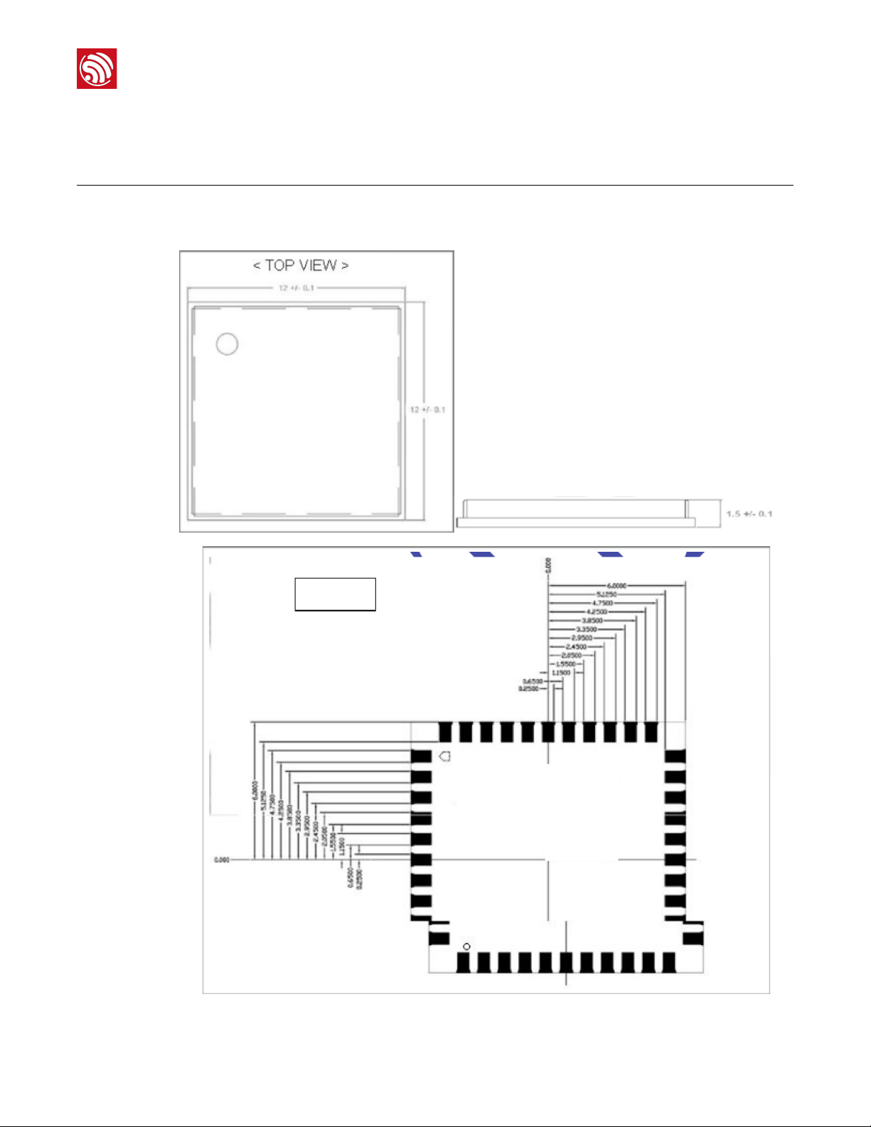
6. Module Dimensions
6. Module Dimensions
6.1. Top View and Side View
! !
!
Espressif
! /!10 13
2017.07
Page 14

!
6. Module Dimensions
6.2. Recommended Footprint
!
Espressif
! /!11 13
2017.07
Page 15

!
7. Packing Information
7. Packing Information
!
Espressif
! /!12 13
2017.07
Page 16

FCC Statement
Any Changes or modifications not expressly approved by the party responsible for compliance could void the
user’s authority to operate the equipment.
This device complies with part 15 of the FCC Rules. Operation is subject to the following two conditions:
(1) This device may not cause harmful interference, and
(2) This device must accept any interference received, including interference that may cause undesired
operation.
FCC Radiation Exposure Statement:
This equipment complies with FCC radiation exposure limits set forth for an uncontrolled environment .This equipment
should be installed and operated with minimum distance 20cm between the radiator& your body.
FCC Label Instructions
The outside of final products that contains this module device must display a label referring to the enclosed
module. This exterior label can use wording such as
: “Contains Transmitter Module
FCC ID:2AC7Z-ESP8089M16“Contains FCC ID:2AC7Z-ESP8089M16 Any similar wording that expresses
the same meaning may be used.
Espr
essif IOT Team"
www.espressif.com
Disclaimer and Copyright Notice
Information in this document, including URL r
notice.
THIS DOCUMENT IS PROVIDED AS IS WITH NO WARRANTIES WHATSOEVER,
INCLUDING ANY WARRANTY OF MERCHANTABILITY, NON-INFRINGEMENT, FITNESS
FOR ANY PARTICULAR PURPOSE, OR ANY WARRANTY OTHERWISE ARISING OUT
OF ANY PROPOSAL, SPECIFICATION OR SAMPLE.
All liability, including liability for infringement of any proprietary rights, relating to use of
information in this document is disclaimed. No licenses express or implied, by estoppel or
otherwise, to any intellectual property rights are granted herein.
The Wi-Fi Alliance Member logo is a trademark of the Wi-Fi Alliance. The Bluetooth logo is
a registered trademark of Bluetooth SIG.
All trade names, trademarks and registered trademarks mentioned in this document are
property of their respective owners, and are hereby acknowledged.
Copyright © 2017 Espressif Inc. All rights reserved.
eferences, is subject to change without
 Loading...