

Page 1

ESP32-S2-WROVER
User Manual
Prelease version 0.1
CONFIDENTIAL
www.espressif.com
Espressif Systems
Copyright © 2019
Page 2

About This Document
This document provides the specifications for the ESP32-S2-WROVER module.
Revision History
For revision history of this document, please refer to the last page.
Documentation Change Notification
Espressif provides email notifications to keep customers updated on changes to technical documentation. Please
subscribe at www.espressif.com/en/subscribe.
Certification
Download certificates for Espressif products from www.espressif.com/en/certificates.
Disclaimer and Copyright Notice
Information in this document, including URL references, is subject to change without notice. THIS DOCUMENT IS
PROVIDED AS IS WITH NO WARRANTIES WHATSOEVER, INCLUDING ANY WARRANTY OF MERCHANTABIL-
ITY, NON-INFRINGEMENT, FITNESS FOR ANY PARTICULAR PURPOSE, OR ANY WARRANTY OTHERWISE
ARISING OUT OF ANY PROPOSAL, SPECIFICATION OR SAMPLE.
All liability, including liability for infringement of any proprietary rights, relating to use of information in this docu-
ment is disclaimed. No licenses express or implied, by estoppel or otherwise, to any intellectual property rights
are granted herein. The Wi-Fi Alliance Member logo is a trademark of the Wi-Fi Alliance. The Bluetooth logo is a
registered trademark of Bluetooth SIG.
All trade names, trademarks and registered trademarks mentioned in this document are property of their respective
owners, and are hereby acknowledged.
Copyright © 2019 Espressif Inc. All rights reserved.
CONFIDENTIAL
Espressif Systems
2
ESP32-S2-WROVER User Manual V0.1
Page 3

1. Module Overview
1. Module Overview
1.1 Features
MCU
• ESP32-S2 embedded, Xtensa®single-core 32-bit
LX7 microprocessor, up to 240 MHz
• 128 KB ROM
• 320 KB SRAM
• 16 KB SRAM in RTC
Wi-Fi
• 802.11 b/g/n
• Bit rate: 802.11n up to 150 Mbps
• A-MPDU and A-MSDU aggregation
• 0.4 µs guard interval support
Hardware
• Interfaces: GPIO, SPI, LCD, UART, I2C, I2S, Cam-
era interface, IR, pulse counter, LED PWM, USB
OTG 1.1, ADC, DAC, touch sensor, temperature
sensor
• 40 MHz crystal oscillator
• 4 MB SPI flash
• 2 MB PSRAM
• Operating voltage/Power supply: 3.0 ~ 3.6 V
•
Operating temperature range: –40 ~ 85 °C
• Dimensions: (18 × 31 × 3.3) mm
Certification
• Green certification: RoHS/REACH
Test
•
Operating frequency range: 2412 ~ 2462 MHz
• HTOL/HTSL/uHAST/TCT/ESD
1.2 Description
ESP32-S2-WROVER is a powerful, generic Wi-Fi MCU module that has a rich set of peripherals. This module is
an ideal choice for a wide variety of application scenarios relating to Internet of Things (IoT), wearable electronics
and smart home.
This module is provided in two versions: one with a PCB antenna, the other with an Dipole antenna.
ESP32-S2-WROVER features a 4 MB external SPI flash and an additional 2 MB SPI Pseudo static RAM (PSRAM).
The information in this datasheet is applicable to both modules.
The ordering information on the two variants of ESP32-S2-WROVER is listed as follows:
Table 1: ESP32-S2-WROVER Ordering Information
Module Chip embedded Flash PSRAM Module dimensions (mm)
CONFIDENTIAL
ESP32-S2-WROVER (PCB)
ESP32-S2-WROVER-I (Dipole)
Notes:
The module with various capacities of flash or flash is available for custom order.
ESP32-S2 4 MB 2 MB (18.00±0.10)×(31.00±0.10)×(3.30±0.10)
At the core of this module is ESP32-S2 *, an Xtensa® 32-bit LX7 CPU that operates at up to 240 MHz. The user
Espressif Systems
3
ESP32-S2-WROVER User Manual V0.1
Page 4

1. Module Overview
can power off the CPU and make use of the low-power co-processor to constantly monitor the peripherals for
changes or crossing of thresholds. ESP32-S2 integrates a rich set of peripherals, ranging from SPI, I²S, UART, I²C,
LED PWM, ADC, DAC, touch sensor, temperature sensor, as well as up to 43 GPIOs. It also includes a full-speed
USB On-The-Go (OTG) interface to enable USB communication.
Note:
* For more information on ESP32-S2, please refer to ESP32-S2 Datasheet.
1.3 Applications
• Generic Low-power IoT Sensor Hub
• Generic Low-power IoT Data Loggers
• Cameras for Video Streaming
• Over-the-top (OTT) Devices
• USB Devices
• Speech Recognition
• Image Recognition
• Mesh Network
• Home Automation
• Smart Home Control Panel
• Smart Building
• Industrial Automation
• Smart Agriculture
• Audio Applications
• Health Care Applications
• Wi-Fi-enabled Toys
• Wearable Electronics
• Retail & Catering Applications
• Smart POS Machines
CONFIDENTIAL
Espressif Systems
4
ESP32-S2-WROVER User Manual V0.1
Page 5

LIST OF TABLES
List of Tables
1 ESP32-S2-WROVER Ordering Information 3
2 Pin Definitions 10
3 Strapping Pins 11
4 Absolute Maximum Ratings 13
5 Recommended Operating Conditions 13
6 DC Characteristics (3.3 V, 25 °C) 13
7 Current Consumption Depending on RF Modes 14
8 Current Consumption Depending on Work Modes 14
9 Wi-Fi RF Standards 15
10 Transmitter Characteristics 15
11 Receiver Characteristics 15
CONFIDENTIAL
Espressif Systems
5
ESP32-S2-WROVER User Manual V0.1
Page 6

LIST OF FIGURES
List of Figures
1 Block Diagram 8
2 Pin Layout of ESP32-S2-WROVER (Top View) 9
3 ESP32-S2-WROVER Schematics 17
4 ESP32-S2-WROVER Peripheral Schematics 18
5 ESP32-S2-WROVER Physical Dimensions 19
6 Recommended PCB Land Pattern 20
7 Reflow Profile 21
CONFIDENTIAL
Espressif Systems
6
ESP32-S2-WROVER User Manual V0.1
Page 7
3. Pin Definitions
PCB Antenna
GND
EN
IO46
IO45
RXD0
TXD0
IO42
IO41
IO40
IO39
IO38
IO37
IO36
IO35
IO34
IO33
1
2
3
4
5
6
7
8
9
10
11
12
13
14
15
16
42
41
40
39
38
37
36
35
34
33
32
31
30
29
28
27
GND
3V3
IO0
IO1
IO2
IO3
IO4
IO5
IO6
IO7
IO8
IO9
IO10
IO11
IO12
IO13
43 GND
17
18
19
IO14
IO15
IO16
20
21
22
IO17
IO18
IO19
23
24
25
IO20
IO21
IO26
26 GND
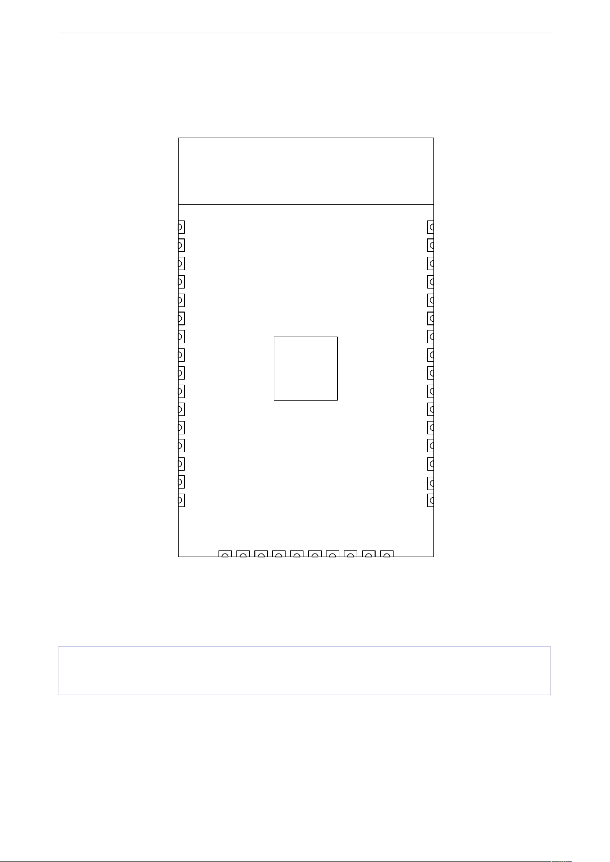
3. Pin Definitions
3.1 Pin Layout
Note:
The pin diagram shows the approximate location of pins on the module. For the actual mechanical diagram, please refer
to Figure 7.1 Physical Dimensions.
CONFIDENTIAL
Figure 2: Pin Layout of ESP32-S2-WROVER (Top View)
3.2 Pin Description
ESP32-S2-WROVER has 42 pins. See pin definitions in Table 2.
Espressif Systems
7
ESP32-S2-WROVER User Manual V0.1
Page 8

3. Pin Definitions
Table 2: Pin Definitions
Name No. Type Function
GND 1 P Ground
3V3 2 P Power supply
IO0 3 I/O/T RTC_GPIO0, GPIO0
IO1 4 I/O/T RTC_GPIO1, GPIO1, TOUCH1, ADC1_CH0
IO2 5 I/O/T RTC_GPIO2, GPIO2, TOUCH2, ADC1_CH1
IO3 6 I/O/T RTC_GPIO3, GPIO3, TOUCH3, ADC1_CH2
IO4 7 I/O/T RTC_GPIO4, GPIO4, TOUCH4, ADC1_CH3
IO5 8 I/O/T RTC_GPIO5, GPIO5, TOUCH5, ADC1_CH4
IO6 9 I/O/T RTC_GPIO6, GPIO6, TOUCH6, ADC1_CH5
IO7 10 I/O/T RTC_GPIO7, GPIO7, TOUCH7, ADC1_CH6
IO8 11 I/O/T RTC_GPIO8, GPIO8, TOUCH8, ADC1_CH7
IO9 12 I/O/T RTC_GPIO9, GPIO9, TOUCH9, ADC1_CH8, FSPIHD
IO10 13 I/O/T RTC_GPIO10, GPIO10, TOUCH10, ADC1_CH9, FSPICS0, FSPIIO4
IO11 14 I/O/T RTC_GPIO11, GPIO11, TOUCH11, ADC2_CH0, FSPID, FSPIIO5
IO12 15 I/O/T RTC_GPIO12, GPIO12, TOUCH12, ADC2_CH1, FSPICLK, FSPIIO6
IO13 16 I/O/T RTC_GPIO13, GPIO13, TOUCH13, ADC2_CH2, FSPIQ, FSPIIO7
IO14 17 I/O/T RTC_GPIO14, GPIO14, TOUCH14, ADC2_CH3, FSPIWP, FSPIDQS
IO15 18 I/O/T RTC_GPIO15, GPIO15, U0RTS, ADC2_CH4, XTAL_32K_P
IO16 19 I/O/T RTC_GPIO16, GPIO16, U0CTS, ADC2_CH5, XTAL_32K_N
IO17 20 I/O/T RTC_GPIO17, GPIO17, U1TXD, ADC2_CH6, DAC_1
IO18 21 I/O/T RTC_GPIO18, GPIO18, U1RXD, ADC2_CH7, DAC_2, CLK_OUT3
IO19 22 I/O/T RTC_GPIO19, GPIO19, U1RTS, ADC2_CH8, CLK_OUT2, USB_D-
IO20 23 I/O/T RTC_GPIO20, GPIO20, U1CTS, ADC2_CH9, CLK_OUT1, USB_D+
IO21 24 I/O/T RTC_GPIO21, GPIO21
IO26 25 I/O/T SPICS1, GPIO26
GND 26 P Ground
IO33 27 I/O/T SPIIO4, GPIO33, FSPIHD
IO34 28 I/O/T SPIIO5, GPIO34, FSPICS0
IO35 29 I/O/T SPIIO6, GPIO35, FSPID
IO36 30 I/O/T SPIIO7, GPIO36, FSPICLK
IO37 31 I/O/T SPIDQS, GPIO37, FSPIQ
IO38 32 I/O/T GPIO38, FSPIWP
IO39 33 I/O/T MTCK, GPIO39, CLK_OUT3
IO40 34 I/O/T MTDO, GPIO40, CLK_OUT2
IO41 35 I/O/T MTDI, GPIO41, CLK_OUT1
IO42 36 I/O/T MTMS, GPIO42
TXD0 37 I/O/T U0TXD, GPIO43, CLK_OUT1
CONFIDENTIAL
RXD0 38 I/O/T U0RXD, GPIO44, CLK_OUT2
IO45 39 I/O/T GPIO45
IO46 40 I GPIO46
High: on, enables the chip.
EN 41 I
Low: off, the chip powers off.
Note: Do not leave the EN pin floating.
Espressif Systems
8
ESP32-S2-WROVER User Manual V0.1
Page 9

3. Pin Definitions
Name No. Type Function
GND 42 P Ground
Notice:
• By default, IO26 is connected to the CS side of the PSRAM. If PSRAM is not a must, IO26 can be used as a regular
GPIO.
• For peripheral pin configurations, please refer to ESP32-S2 Datasheet.
3.3 Strapping Pins
ESP32-S2 has three strapping pins: GPIO0, GPIO45, GPIO46. The pin-pin mapping between ESP32-S2 and the
module is as follows, which can be seen in Chapter 5 Schematics:
• GPIO0 = IO0
• GPIO45 = IO45
• GPIO46 = IO46
Software can read the values of corresponding bits from register ”GPIO_STRAPPING”.
During the chip’s system reset (power-on-reset, RTC watchdog reset, brownout reset, analog super watchdog
reset, and crystal clock glitch detection reset), the latches of the strapping pins sample the voltage level as strapping
bits of ”0” or ”1”, and hold these bits until the chip is powered down or shut down.
IO0, IO45 and IO46 are connected to the internal pull-up/pull-down. If they are unconnected or the connected
external circuit is high-impedance, the internal weak pull-up/pull-down will determine the default input level of these
strapping pins.
To change the strapping bit values, users can apply the external pull-down/pull-up resistances, or use the host
MCU’s GPIOs to control the voltage level of these pins when powering on ESP32-S2.
After reset, the strapping pins work as normal-function pins.
Refer to Table 3 for a detailed boot-mode configuration of the strapping pins.
Table 3: Strapping Pins
VDD_SPI Voltage
Pin Default 3.3 V 1.8 V
2
IO45
Pin Default SPI Boot Download Boot
IO0 Pull-up 1 0
CONFIDENTIAL
IO46 Pull-down Don’t-care 0
Pin Default Enabled Disabled
IO46 Pull-down See the fourth note See the fourth note
Pull-down 0 1
Booting Mode
Enabling/Disabling ROM Code Print During Booting
1
3 4
Espressif Systems
9
ESP32-S2-WROVER User Manual V0.1
Page 10

3. Pin Definitions
Note:
1. Firmware can configure register bits to change the settings of ”VDD_SDIO Voltage”.
2. Internal pull-up resistor (R1) for IO45 is not populated in the module, as the flash and SRAM in ESP32-S2-WROVER
work at 3.3 V by default (output by VDD_SPI). Please make sure IO45 will not be pulled high when the module is
powered up by external circuit.
3. ROM code can be printed over TXD0 (by default) or DAC_1 (IO17), depending on the eFuse bit.
4. When eFuse UART_PRINT_CONTROL value is:
0, print is normal during boot and not controlled by IO46.
1 and IO46 is 0, print is normal during boot; but if IO46 is 1, print is disabled.
2 and IO46 is 0, print is disabled; but if IO46 is 1, print is normal.
3, print is disabled and not controlled by IO46.
CONFIDENTIAL
Espressif Systems
10
ESP32-S2-WROVER User Manual V0.1
Page 11

4. Electrical Characteristics
4. Electrical Characteristics
4.1 Absolute Maximum Ratings
Table 4: Absolute Maximum Ratings
Symbol Parameter
VDD33 Power supply voltage
T
ST O RE
Storage temperature
Min Max
–0.3 3.6
–40 150
Unit
V
°C
4.2 Recommended Operating Conditions
Table 5: Recommended Operating Conditions
Symbol Parameter
VDD33 Power supply voltage
I
V DD
T Operating temperature
Humidity Humidity condition
Current delivered by external power supply
Min Typ Max
3.0 3.3 3.6
0.5 — —
–40 —
— 85 —
85
Unit
V
A
°C
%RH
4.3 DC Characteristics (3.3 V, 25 °C)
Table 6: DC Characteristics (3.3 V, 25 °C)
Symbol Parameter
C
IN
V
IH
V
IL
I
IH
I
IL
V
OH
V
OL
I
OH
I
OL
R
P U
R
P D
CONFIDENTIAL
V
IH _nRST
V
IL_nRS T
Pin capacitance
High-level input voltage
Low-level input voltage
High-level input current
Low-level input current
High-level output voltage
Low-level output voltage
High-level source current (VDD = 3.3 V, VOH>=
2.64 V, PAD_DRIVER = 3)
Low-level sink current (VDD = 3.3 V, VOL=
0.495 V, PAD_DRIVER = 3)
Pull-up resistor
Pull-down resistor
Chip reset release voltage
Chip reset voltage
Min Typ Max
— 2 —
0.75 × VDD — VDD + 0.3
–0.3 — 0.25 × VDD
— — 50
— — 50
0.8 × VDD — —
— — 0.1 × VDD
— 40 —
— 28 —
— 45 —
— 45 —
0.75 × VDD — VDD + 0.3
–0.3 — 0.25 × VDD
Unit
pF
V
V
nA
nA
V
V
mA
mA
kΩ
kΩ
V
V
Note:
VDD is the I/O voltage for a particular power domain of pins.
Espressif Systems
11
ESP32-S2-WROVER User Manual V0.1
Page 12

4. Electrical Characteristics
4.4 Current Consumption Characteristics
With the use of advanced power-management technologies, ESP32-S2-WROVER can switch between different
power modes. For details on different power modes, please refer to Section RTC and Low-Power Management in
ESP32-S2 Datasheet.
The current consumption measurements are taken with a 3.3 V supply at 25 °C of ambient temperature at the RF
port. All transmitters’ measurements are based on a 50% duty cycle.
Table 7: Current Consumption Depending on RF Modes
Work mode Description Average Peak
190 mA 310 mA
145 mA 220 mA
135 mA 200 mA
120 mA 160 mA
Active (RF working)
TX
RX
802.11b, 20 MHz, 1 Mbps, @21.14 dBm
802.11g, 20 MHz, 54 Mbps, @22.75dBm
802.11n, 20 MHz, MCS7, @23.06dBm
802.11n, 40 MHz, MCS7, @22.53 dBm
802.11b/g/n, 20 MHz 63 mA 63 mA
802.11n, 40 MHz 68 mA 68 mA
Note:
The current consumption figures for in RX mode are for cases when the peripherals are disabled and the CPU idle.
Table 8: Current Consumption Depending on Work Modes
Work mode Description Power consumption (Typ)
Modem-sleep
Light-sleep — 550 µA
Deep-sleep
Power off CHIP_PU is set to low level, the chip is powered off. 0.5 µA
Note:
• The current consumption figures in Modem-sleep mode are for cases where the CPU is powered on and the cache
idle.
The CPU is
powered on
The ULP co-processor is powered on. 220 µA
240 MHz 21 mA
160 MHz 17 mA
Normal speed: 80 MHz 14 mA
ULP sensor-monitored pattern 7 µA @1% duty
RTC timer + RTC memory 10 µA
RTC timer only 5 µA
• When Wi-Fi is enabled, the chip switches between Active and Modem-sleep modes. Therefore, current consump-
tion changes accordingly.
• In Modem-sleep mode, the CPU frequency changes automatically. The frequency depends on the CPU load and
CONFIDENTIAL
the peripherals used.
• During Deep-sleep, when the ULP co-processor is powered on, peripherals such as GPIO and I²C are able to
operate.
• The ”ULP sensor-monitored pattern” refers to the mode where the ULP coprocessor or the sensor works periodi-
cally. When touch sensors work with a duty cycle of 1%, the typical current consumption is 7 µA.
Espressif Systems
12
ESP32-S2-WROVER User Manual V0.1
Page 13

4. Electrical Characteristics
4.5 Wi-Fi RF Characteristics
4.5.1 Wi-Fi RF Standards
Table 9: Wi-Fi RF Standards
Name Description
Operating frequency range
Wi-Fi wireless standard IEEE 802.11b/g/n
Data rate
Antenna type PCB antenna, Dipole antenna
1. Device should operate in the frequency range allocated by regional regulatory authorities. Target operating frequency
range is configurable by software.
For the modules that use Dipole antennas, the output impedance is 50 Ω. For other modules without Dipole antennas,
2.
users do not need to concern about the output impedance.
note1
2412 ~ 2462 MHz
11b: 1, 2, 5.5 and 11 Mbps
20 MHz
11g: 6, 9, 12, 18, 24, 36, 48, 54 Mbps
11n: MCS0-7, 72.2 Mbps (Max)
40 MHz 11n: MCS0-7, 150 Mbps (Max)
4.5.2 Transmitter Characteristics
Table 10: Transmitter Characteristics
Parameter Rate Typ Unit
TX Power
note1
11b, 1 Mbps
11g, 6 Mbps
11n, HT20, MCS0
11n, HT40, MCS0
1. Target TX power is configurable based on device or certification requirements.
4.5.3 Receiver Characteristics
Table 11: Receiver Characteristics
21.14
22.75
23.06
22.53
dBm
Espressif Systems
Parameter Rate Typ Unit
RX Sensitivity 1 Mbps –97 dBm
2 Mbps –95
5.5 Mbps –93
11 Mbps –88
6 Mbps –92
9 Mbps –91
13
ESP32-S2-WROVER User Manual V0.1
Page 14

4. Electrical Characteristics
Parameter Rate Typ Unit
RX Maximum Input Level 11b, 1 Mbps 5 dBm
Adjacent Channel Rejection 11b, 11 Mbps 35 dB
12 Mbps –89
18 Mbps –87
24 Mbps –84
36 Mbps –80
48 Mbps –76
54 Mbps –75
11n, HT20, MCS0 –92
11n, HT20, MCS1 –88
11n, HT20, MCS2 –85
11n, HT20, MCS3 –83
11n, HT20, MCS4 –79
11n, HT20, MCS5 –75
11n, HT20, MCS6 –74
11n, HT20, MCS7 –72
11n, HT40, MCS0 –89
11n, HT40, MCS1 –86
11n, HT40, MCS2 –83
11n, HT40, MCS3 –80
11n, HT40, MCS4 –76
11n, HT40, MCS5 –72
11n, HT40, MCS6 –71
11n, HT40, MCS7 –69
11b, 11 Mbps 5
11g, 6 Mbps 5
11g, 54 Mbps 0
11n, HT20, MCS0 5
11n, HT20, MCS7 0
11n, HT40, MCS0 5
11n, HT40, MCS7 0
11g, 6 Mbps 31
11g, 54 Mbps 14
11n, HT20, MCS0 31
11n, HT20, MCS7 13
11n, HT40, MCS0 19
11n, HT40, MCS7 8
CONFIDENTIAL
Espressif Systems
14
ESP32-S2-WROVER User Manual V0.1
Page 15

7. Physical Dimensions and PCB Land Pattern
31.00
18.00
0.80
3.30
1.50
0.45
0.90
0.85
15.45
10.19
4.00
4.00
2.25
0.45
ESP32-S2-WROVER Dimensions
Unit: mm
Tolerance: +/-0.10mm
Top View
Side View
Bottom View
6.30
8.35
23.10
15.84
19.30
10.44
1.50
1.00
0.50
1.00
0.50
0.85
0.90
0.90
1.00
2.25
7. Physical Dimensions and PCB Land Pattern
7.1 Physical Dimensions
Figure 5: ESP32-S2-WROVER Physical Dimensions
Note:
• Soldering the EPAD to the ground of the base board is not a must, though doing so can get optimized thermal
performance. If users do want to solder it, they need to ensure that the correct quantity of soldering paste is applied.
• To ensure the power supply to the ESP32-S2 chip during power-up, it is advised to add an RC delay circuit at the
EN pin. The recommended setting for the RC delay circuit is usually R = 10 kΩ and C = 0.1 µF. However, specific
parameters should be adjusted based on the power-up timing of the module and the power-up and reset sequence
timing of the chip. For ESP32-S2’s power-up and reset sequence timing diagram, please refer to Section Power
CONFIDENTIAL
Scheme in ESP32-S2 Datasheet.
Espressif Systems
15
ESP32-S2-WROVER User Manual V0.1
Page 16

7. Physical Dimensions and PCB Land Pattern
42x0.90
42x1.50
0.50
0.50
1.00
2.25
1.50
1.50
15.45
Antenna Area
18.00
31.00
Unit: mm
6.30
Copper
1
17
26
42
4.10
4.10
1.10
0.40
1.10
0.40
Via for thermal pad
7.81
7.2 Recommended PCB Land Pattern
Figure 6: Recommended PCB Land Pattern
CONFIDENTIAL
Espressif Systems
16
ESP32-S2-WROVER User Manual V0.1
Page 17

8. Product Handling
50
150
0
25
1 ~ 3℃/s
0
200
250
200
-1 ~ -5℃/s
Cooling zone
100
217
50
100 250
Reflow zone
!217℃ 60 ~ 90s
Temperature (℃)
Preheating zone
150 ~ 200℃ 60 ~ 120s
Ramp-up zone
Peak Temp.
235 ~ 250℃
Soldering time
> 30s
Time (sec.)
Ramp-up zone — Temp.: <150℃ Time: 60 ~ 90s Ramp-up rate: 1 ~ 3℃/s
Preheating zone — Temp.: 150 ~ 200℃ Time: 60 ~ 120s Ramp-up rate: 0.3 ~ 0.8℃/s
Reflow zone — Temp.: >217℃ 7LPH60 ~ 90s; Peak Temp.: 235 ~ 250℃ (<245℃ recommended) Time: 30 ~ 70s
Cooling zone — Peak Temp. ~ 180℃ Ramp-down rate: -1 ~ -5℃/s
Solder — Sn&Ag&Cu Lead-free solder (SAC305)
8. Product Handling
8.1 Storage Condition
The products sealed in Moisture Barrier Bag (MBB) should be stored in a noncondensing atmospheric environment
of < 40 °C/90%RH.
MSL 3 and floorlife: 168 hrs �30 °C/60%RH
8.2 ESD
• Human body model (HBM): 2000 V
• Charged-device model (CDM): 500 V
• Air discharge: 8000 V
• Contact discharge: 6000 V
8.3 Reflow Profile
CONFIDENTIAL
Espressif Systems
Figure 7: Reflow Profile
17
ESP32-S2-WROVER User Manual V0.1
Page 18

9. MAC Addresses and eFuse
9. MAC Addresses and eFuse
The eFuse in ESP32-S2 has been burnt into 48-bit mac_address. The actual addresses the chip uses in station
and AP modes correspond to mac_address in the following way:
• Station mode: mac_address
• AP mode: mac_address + 1
There are seven blocks in eFuse for users to use. Each block is 256 bits in size and has independent write/read
disable controller. Six of them can be used to store encrypted key or user data, and one is only used to store user
data.
CONFIDENTIAL
Espressif Systems
18
ESP32-S2-WROVER User Manual V0.1
Page 19

Revision History
Revision History
Date Version Release notes
2019.09 V0.1 Preliminary release
FCC Statement
Any Changes or modifications not expressly approved by the party responsible for
compliance could void the user’s authority to operate the equipment.
This device complies with part 15 of the FCC Rules. Operation is subject to the
following two conditions:
(1) This device may not cause harmful interference, and (2) This device must accept
any interference received, including interference that may cause undesired operation.
FCC Radiation Exposure Statement:
This equipment complies with FCC radiation exposure limits set forth for an
uncontrolled environment .This equipment should be installed and operated with
minimum distance 20cm between the radiator& your body.
CONFIDENTIAL
Espressif Systems
19
ESP32-S2-WROVER User Manual V0.1
Page 20

Regulatory Module Integration Instructions
2.2 List of applicable FCC rules
This device complies with part 15.247 of the FCC Rules.
2.3 Summarize the specific operational use conditions
This module can be used in household electrical appliances as well as lighting
equipments. The input voltage to the module should be nominally 3.0~3.6 VDC ,typical
value 3.3VDC and the ambient temperature of the module should not exceed 85℃.
This module us
Dipole antenan with maximum gain is 2.33dBi .Other antenna arrangement is not covered
by this certification.The antenna is not field replaceable. If the antenna needs to be changed,
the certification
2.4 Limited module procedures
Not applicable
2.5 Trace antenna designs
Not applicable
2.6 RF exposure considerations
This equipment complies with FCC radiation exposure limits set forth for an uncontrolled
ing two kinds of antennas ,PCB antenan with maximum gain is 3.40dBi .
should be re-applied.
environment .
20cm between the radiator& your body. If the device built into a host as a portable usage,
the additional RF exposure evaluation may be required as specified by§ 2.1093.
This equipment should be installed and operated with minimum distance
Page 21

2.7 Antennas
Module contains one PCB antenna and Dipole antenna.
2.8 Label and compliance information
The outside of final products that contains this module device must display a label
referring to the enclosed module. This exterior label can use wording such as: “Contains
Transmitter Module FCC ID: 2AC7Z-ESP32S2WROVER ”,or “Contains
FCC ID: 2AC7Z-ESP32S2WROVER ”, Any similar wording that expresses the same meaning may
be used.
2.9 Information on test modes and additional testing requirements
a) The modular transmitter has been fully tested by the module grantee on the required
number of channels, modulation types, and modes, it should not be necessary for the
host installer to re-test all the available transmitter modes or settings. It is
recommended that the host product manufacturer, installing the modular transmitter,
perform some investigative measurements to confirm that the resulting composite
system does not exceed the spurious emissions limits or band edge limits (e.g., where a
different antenna may be causing additional emissions).
b) The testing should check for emissions that may occur due to the intermixing of
emissions with the other transmitters, digital circuitry, or due to physical properties of
the host product (enclosure). This investigation is especially important when integrating
multiple modular transmitters where the certification is based on testing each of them in
a stand-alone configuration. It is important to note that host product manufacturers
should not assume that because the modular transmitter is certified that they do not
Page 22

WRG1 User Manual
have any responsibility for final product compliance.
c) If the investigation indicates a compliance concern the host product manufacturer is
obligated to mitigate the issue. Host products using a modular transmitter are subject to
all the applicable individual technical rules as well as to the general conditions of
operation in Sections 15.5, 15.15, and 15.29 to not cause interference. The operator of
the host product will be obligated to stop operating the device until the interference has
been corrected
Below are steps for TX verification:
wpriv mp_start //enter MP mode
iwpriv mp_channel 1 //set channel to 1 . 2, 3, 4~11 etc.
iwpriv mp_bandwidth 40M=0,shortGI=0 //40M=0 set 20M mode and long GI,
40M=1 set 40M mode
iwpriv mp_ant_tx a //select antenna A for operation
iwpriv mp_txpower patha=44,pathb=44 //set path A and path B Tx power level
iwpriv mp_rate 108 //set OFDM data rate to 54Mbps,ex:
CCK 1M = 2, CCK 5.5M = 11, KK, OFDM54M = 108 N Mode: MCS0 = 128, MCS1
= 129…..etc.
iwpriv mp_ctx background,pkt //start packet continuous Tx
iwpriv mp_ctx stop //stop continuous Tx
2.10 Additional testing, Part 15 subpart B disclaimer
The final host / module combination need to be evaluated against the FCC Part 15B
criteria for unintentional radiators in order to be properly authorized for operation as a Part
15 digital device.
Page 23

The host integrator installing
composite product complies with the FCC requirements by a technical assessment or
evaluation to the FCC rules, including the transmitter operation and should refer to
guidance in KDB 996369.
Frequency spectrum to be investigated
For host products with certified modular transmitter, the frequency range of investigation
of the composite system is specified by rule in Sections 15.33(a)(1) through (a)(3), or the
range applicable to the digital device, as shown in Section 15.33(b)(1), whichever is the
higher frequency range of investigation.
Operating the host product
this module into their product must ensure that the final
When testing the host product, all the transmitters must be operating.The transmitters can
be enabled by using publicly-available drivers and turned on, so the transmitters are
active. In certain conditions it might be appropriate to use a technology-specific call box
(test set) where accessory devices or drivers are not available.
When testing for emissions from the unintentional radiator, the transmitter shall be placed
in the receive mode or idle mode, if possible. If receive mode only is not possible then, the
radio shall be passive (preferred) and/or active scanning. In these cases, this would need
to enable activity on the communication BUS (i.e., PCIe, SDIO, USB) to ensure the
unintentional radiator circuitry is enabled. Testing laboratories may need to add
attenuation or filters depending on the signal strength of any active beacons (if applicable)
from the enabled radio(s). See ANSI C63.4, ANSI C63.10 and ANSI C63.26 for further
Page 24

general testing details.
 Loading...