

Page 1

ESP32-LyraTD-SYNA
User Guide
Version 1.0
Espressif Systems
Copyright © 2019
Page 2

About This Guide
This document helps you to get started with the ESP32-LyraTD-SYNA development board.
Release Notes
Documentation Change Notification
Espressif provides email notifications to keep customers updated on changes to
technical documentation. Please subscribe at https://www.espressif.com/en/subscribe.
Certification
Download certificates for Espressif products from https://www.espressif.com/en/
certificates.!
Date
Version
Release notes
2019.09
V1.0
Initial release.
Page 3

Table of Contents
1. Overview 1 ................................................................................................................................
1.1. ESP32-LyraTD-SYNA! 1".................................................................................................................
1.2. Hardware Resources! 1"..................................................................................................................
2. Configuring for AVS 3 ...............................................................................................................
2.1. Software Preparation! 3".................................................................................................................
2.2. Hardware Preparation! 3"................................................................................................................
2.3. Flashing the Firmware! 4"................................................................................................................
2.3.1. Driver Installation! 4"..........................................................................................................
2.3.2. Flashing ESP32! 4".............................................................................................................
2.4. Network Configuration! 7"...............................................................................................................
2.4.1. Wi-Fi Networking! 7"..........................................................................................................
2.5. Interactive Function! 10"..................................................................................................................
2.5.1. Voice Recognition! 10".......................................................................................................
2.5.2. Buttons! 10".......................................................................................................................
A. Appendix - Schematics 11.......................................................................................................
Page 4
!
1.Overview
1. Overview
ESP32-LyraTD-SYNA is one of Espressif’s Audio Development Board based on ESP32
MCU and Synaptics DSP. It is an Acoustic Echo Cancelation (AEC) solution, supporting
voice recognition and voice wake-up. Audio files in the format of WAV, MP3, AAC, FLAC,
OPUS and OGG can be decoded and encoded without quality loss. It also supports
connection to Amazon’s AVS (Alexa Voice Service), Google's Dialogflow and Google's GVA
(Google Voice Assistant).
1.1. ESP32-LyraTD-SYNA
ESP32-LyraTD-SYNA is based on ESP32-WROVER-B, a BT/Wi-Fi combo module, and a
digital signal processor (DSP) that features a two-microphone array for noise reduction and
echo cancelation, as well as a Coder-Decoder (CODEC) that includes two pairs of DACs &
ADCs with high sampling rates.
!
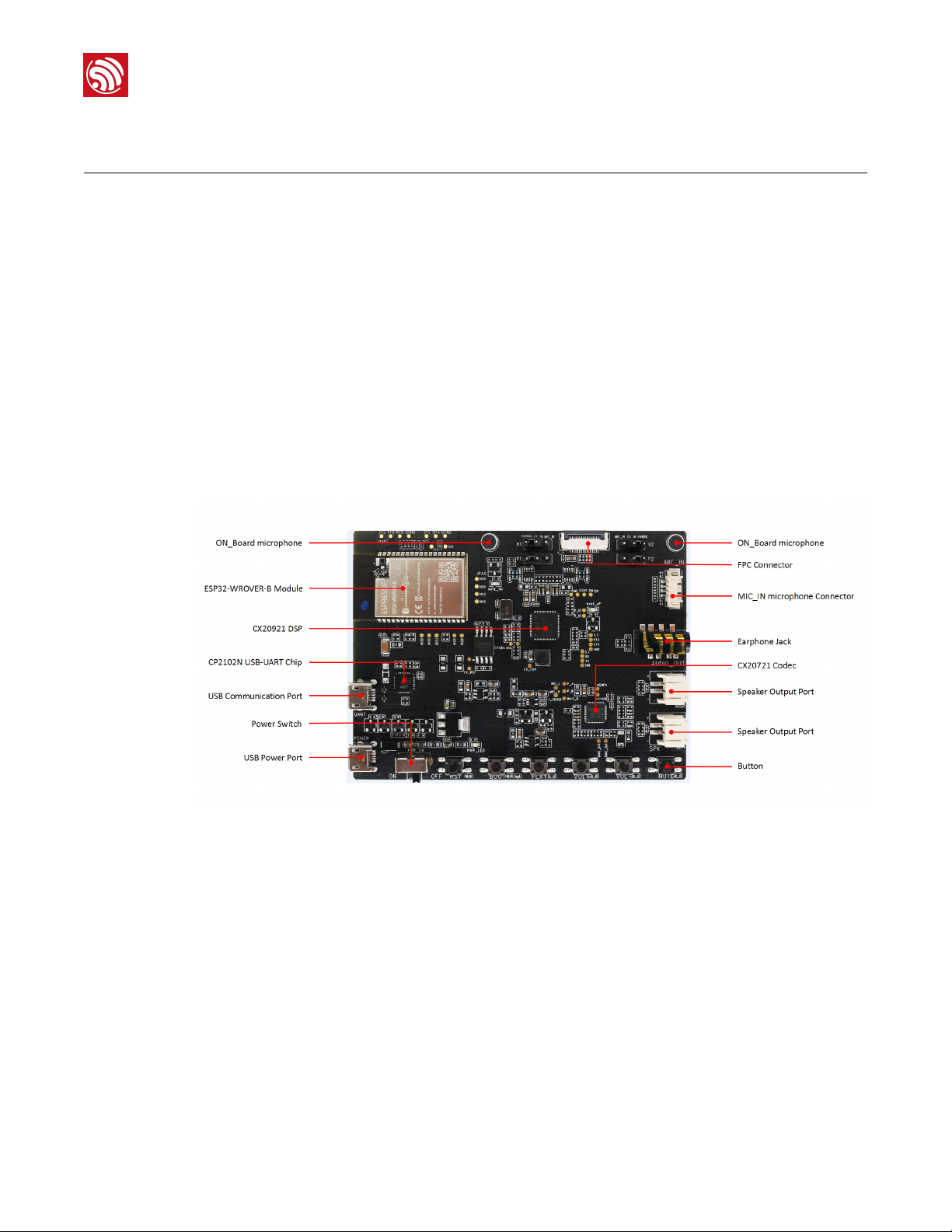
Figure 1-1. ESP32-LyraTD-SYNA
1.2. Hardware Resources
1. USB Power Port
Provides power supply to the whole system. It is recommended that the system be
connected to a power adapter for sufficient current supply.
2. ESP32-WROVER-B module
This is a powerful, general-purpose, Wi-Fi+BT+BLE dual core MCU module, targeting a
wide variety of applications ranging from low-power sensor networks to the most
demanding tasks, such as voice encoding/decoding, music streaming and runs voice
assistant client SDK.
Espressif
! /171
2019.09
Page 5

!
1.Overview
3. CX20921 DSP
CX20921 is a dual core, far field voice input processor which supports Smart Source
Pickup(SSP) noise suppression and various functionalities such as voice control, voice
search, Voice over Internet Protocol (VOlP) and acoustic echo cancellation (AEC). This
audio DSP is used for wake-word detection. It captures audio data from two external
microphones.
4. CX20721 codec
CX20721 is an audio Coder-Decoder which has integrated AudioSmart Class-D with
2.8W per channel.
5. CP2102N USB-UART Chip
An upgraded version of the CP2102 chip supports USB-to-UART conversion.
6. USB Communication Port
This is a normal USB communication port between PC and ESP32 module.
7. ON-Board microphone
There are two types of microphone connection, on-board and by MIC-IN connector.
8. MIC-IN microphone connector
Supports two external microphones.
9. FPC connector
This connection is reserved for connecting external sub board consisting of more
devices, such as microphone array, buttons and LEDs etc.
10. Earphone jack
Used for plugging in earphones. Audio output is via codec.
11. Speaker output port
Supports two external speakers output via codec.
12. Button
The six buttons figure different functions, such as RST, BOOT, PLAY, VOL+/-, MUTE etc.
⚠ Notice:
The IC design of this chip is a little different from CP2102.
Espressif
! /172
2019.09
Page 6

!
2. Configuring for AVS
2. Configuring for AVS
2.1. Software Preparation
1. Installing Flash Download Tool
Linux/macOS/Windows users can use the terminal to flash firmware. For more details,
please check ESP-IDF Programming Guide.
Windows users may also use a graphical tool to flash firmware onto the board using the
Flash Download Tool.
2. Downloading Firmware
Please follow the build instructions of the Alexa SDK from the Github page: https://
github.com/espressif/esp-va-sdk.
3. Debugging Tool
Use serial monitor/console that suits your development environment at baud rate of
115200.
4. App for Provisioning
In order to run Alexa you need to provision LyraTD-SYNA with Alexa credentials and
network settings (Wi-Fi SSID and passphrase).
•
Android APK: https://play.google.com/store/apps/details?
id=com.espressif.provbleavs
• iOS: https://apps.apple.com/us/app/esp-alexa/id1464127534
2.2. Hardware Preparation
• 1 x PC (Linux Operating System is recommended).
•
1 x ESP32-LyraTD-SYNA.
• 2 x Micro USB cables (one is for the USB power supply).
• 1 x Speaker or 1 x earphone.
⚠ Notice:
The GitHub repository uses Espressif’s wake-word engine (WWE) for processing the ‘Alexa’ wakeword. This allows easy evaluations. For production use cases, please reach out to
sales@espressif.com or your Synaptics sales representative to obtain an Amazon certified wake-word
engine.
Espressif
! /173
2019.09
Page 7

!
2. Configuring for AVS
2.3. Flashing the Firmware
This document captures the process of flashing the firmware on Windows. Please refer to
the ESP-VA-SDK repository on Github for setup on other platforms.
2.3.1. Driver Installation
Connect the board to a PC with a Micro-USB cable and install the USB-to-UART driver.
2.3.2. Flashing ESP32
!
Figure 2-1. Flash Download Tool
• In order to build examples of esp-va-sdk, please follow the instructions mentioned on
the GitHub page.
• Once you build the Alexa firmware, you will generate three artifacts: bootloader.bin,
partitions.bin and alexa.bin.
• For Flash Download Tool users, follow the instructions given below.
1. Run Flash Download Tool, and click on “ESP32 Download Tool” at the interface.
See Figure 2-1 above.
2. Then you will see the interface shown in Figure 2-2 below.
Espressif
! /174
2019.09
Page 8

!
2. Configuring for AVS
!
Figure 2-2. ESP32 Download Tool
3. Select the binary files (mentioned in table below) and set appropriate address in the
tool as shown in Figure 2-3.
Binary Files
Address
Function
bootloader.bin
0x1000
basic configuration
partitions.bin
0x8000
basic configuration
alexa.bin
0x10000
audio application
Espressif
! /175
2019.09
Page 9

!
2. Configuring for AVS
!
Figure 2-3. Flashing Configuration
4. The SPI Download configuration on the ESP32 Download Tool is shown in Figure
2-3. Select “80 MHz” for “SPI SPEED”; select “DIO” for “SPI MODE”; and select
“128 Mbit” for “FLASH SIZE”.
5. Select the COM port in line with the one used by the PC; select “1152000” as a baud
rate.
6. Click the “START” button on the ESP32 Flash Download Tool to start downloading
the firmware.
7. Wait for the download to finish. See Figure 2-4.
!
Figure 2-4. Downloading Firmware
Espressif
! /176
2019.09
Page 10

!
2. Configuring for AVS
2.4. Network Configuration
2.4.1. Wi-Fi Networking
1. After successfully downloading the firmware, power on the board again by pressing the
EN button.
2. To configure the network for the first time:
• Turn on the bluetooth in your phone. Open Espressif’s Alexa programming app and
click on Provision New Device. Make sure your phone has internet connectivity.
!
Figure 2-5. Provision New Device
• The provisioning happens over BLE (Bluetooth Low Energy). Android mandates
applications to have Location permission for accessing BLE. Please provide the
permission when the pop-up shows up.
•
You will see the list of available devices that needs to be provisioned, namely ESP-
Alexa-WXYZ. Select the device that you wish to provision.
📖 Note:
Terminal users can follow the flashing instructions as available on the GitHub page.
Espressif
! /177
2019.09
Page 11

!
2. Configuring for AVS
!
Figure 2-6. List of available devices
• Next step is to login to your amazon account.
!
Figure 2-7. Login to your amazon
•
After successful login and authorization, you will be shown a list of Wi-Fi networks in
the vicinity. Choose the network that you wish the device to connect to. Once
Espressif
! /178
2019.09
Page 12

!
2. Configuring for AVS
selected, enter the passphrase of that Wi-Fi network and click on the provision
button.
!
Figure 2-8. Available Wi-Fi networks
!
Figure 2-9. Enter your passphrase
• On successfully connecting to the Wi-Fi network, after provisioning, the DSP and
Alexa will be initialized, and ready to take voice commands.
Espressif
! /179
2019.09
Page 13

!
2. Configuring for AVS
2.5. Interactive Function
2.5.1. Voice Recognition
•
Once all initialization are done, the device is ready. You can either use "PLAY" button on
the board (Tap-To-Talk) or say "Alexa" to start a conversation. For Tap-to-Talk, press and
release the button and speak.
•
You can now ask any command like:
-
Tell me a joke.
-
How is the weather?
-
Will it rain today?
-
Sing a song.
-
Play TuneIn radio.
-
Set volume level to 7.
2.5.2. Buttons
• The “PLAY” button can be used as tap-to-talk. The same button can also be used to
disable an Alarm/Timer.
• The “Vol+” and “Vol-” buttons can be used to adjust the volume of the sound. Press
them repeatedly until you reach the desired sound volume.
• The "Mute" button can be used to mute/unmute the device.
• To reset to factory settings, press "Vol+" and "Vol-" button together for about 10
seconds.
Espressif
! /1710
2019.09
Page 14

!
Appendix A
A. Appendix - Schematics
! !
5
5
4
4
3
3
2
2
1
1
D D
C C
B B
A A
ESP32
Power Block:
System Block:
DSP
CX20921
Codec
CX22721
MIC*2
Keys
SPK*2
EN Key
RST
BOOT Key
BOOT
USBtoUART
TX/RX
USB
CNN
D+/D-
Key*4
CNN(Reserved
for LED,Key,MIC)
I2C&ADC
MIC
OUT+/-
INT+RST+I2C
+I2S_CX_TX
IRQ+EAPD+I2C
+I2S_ESP_TX
I2S_AEC
VCC
AP7361C-33
-ER-7/13
USB
CNN
ESP32
3.3V
LDO
3.3V
DSP
CX20921
3.3V
Codec
CX22721
LDO
LDO
1.8V
VCC
Title
Size
Document Number Rev
Date: Sheet of
<01_Block> 1.3
ESP32-LYRATD-SYNA
C
1 6Friday, August 30, 2019
Title
Size
Document Number Rev
Date: Sheet of
<01_Block> 1.3
ESP32-LYRATD-SYNA
C
1 6Friday, August 30, 2019
Title
Size
Document Number Rev
Date: Sheet of
<01_Block> 1.3
ESP32-LYRATD-SYNA
C
1 6Friday, August 30, 2019
Espressif
! /!11 17
2019.09
Page 15

!
Appendix A
! !
5
5
4
4
3
3
2
2
1
1
D D
C C
B B
A A
ESP32 Module:
Button Array
USB<->UART:
JTAG
MTDI
MTCK
MTMS
MTDO
UART I2C
I2C:SCL
I2C:SDA
I2S
Automatic & Button Download:
Auto program
DTR RTS--> EN_Auto IO0_IO2_Auto
1 1 1 1
0 0 1 1
1 0 0 1
0 1 1 0
DSP GPIO
DSP_I2S_LRCK : IO32
Codec_SPK_MUTE:IO22
PJ_DET:IO21
Codec_I2S_BCLK:IO5
Codec_I2S_FS:IO25
Codec_I2S_SDI0:IO26
Codec_I2S_MCLK:IO0
Codec_EAPD:IO4
DSP_I2S_DO : IO35
DSP_I2S_BCLK : IO33
DSP RESET : IO19
I2C_SCL:IO23
I2C_SDA:IO18
MUTE_ON_OFF:IO27
USB:
3.3V/800mA
Power Supply for ESP32:
EN
SENSOR_VP
SENSOR_VN_ADC
IO34
IO35
IO32
IO33
IO25
IO26
IO27
IO14
3V3
IO13
DGND
IO22
TXD0
RXD0
IO21
IO19
IO18
IO4
IO0
IO5
IO23
Module_NC
IO15
IO2
DGND
SHD/SD2
SWP/SD3
SCS/CMD SCK/CLK
SDO/SD0
SDI/SD1
IO17_NC
IO16_NC
DGND
IO12
IO12
IO13
IO14
IO15
TXD0
RXD0
IO23
IO18
IO35
IO32
IO33
IO0
IO5
IO25
IO26
IO23
IO18
Module_NC
3V3
IO26
IO27
IO34
IO22
DGND
IO12
IO17_NC
IO16_NC
DGND
IO19
IO25
IO2
EN
SENSOR_VP
SENSOR_VN_ADC
IO35
IO32
IO33
IO14
IO23
TXD0
RXD0
IO21
IO18
IO4
IO0
DGND
IO13
SHD/SD2
SWP/SD3
SCS/CMD
SCK/CLK
SDO/SD0
SDI/SD1
IO15
IO5
SENSOR_VN
IO18
IO33
IO32
SENSOR_VP
IO22
IO21
IO5
IO25
IO26
IO0
IO4
IO35
IO19
IO23
IO27
D-
D+
USB_DP
USB_DN
REGIN
TXD
RXD0
USB_DN
RST#
ACTIVE
TXD0
USB_DP
DTR
RTS
IO0_IO2_Auto
IO0_IO2_KEY
IO2
IO0
EN
EN_KEY
EN_Auto
DTR
RTS
EN_Auto
IO0_IO2_Auto
EN
SENSOR_VN SENSOR_VN_ADC
DGND
GND
DGND
VDD33
DGND
VDD33
VDD33
DGND
GNDGND GND
GND
VUSB
GND
VBUS0
VUSB
GND
GND
GND
VBUS0
GND
GND
VDD33
GND
VDD33
VCC
GNDGND
VUSB
GND
VCC
GNDGND GND
VDD33
VDD33
GND
GND
VDD33
DGND
VDD33
DGND
SENSOR_VN 3
IO18
3,5,6
IO33 5
IO32 5
CX_GPIO_1 5
IO23 3,5,6
IO226IO21
6
IO5 6
IO256IO266IO0
6
IO4
6
IO35 5
IO19
5
IO27 3,5
Title
Size
Document Number Rev
Date: Sheet of
<02_Power_MCU> 1.3
ESP32-LYRATD-SYNA
C
2 6Friday, August 30, 2019
Title
Size
Document Number Rev
Date: Sheet of
<02_Power_MCU> 1.3
ESP32-LYRATD-SYNA
C
2 6Friday, August 30, 2019
Title
Size
Document Number Rev
Date: Sheet of
<02_Power_MCU> 1.3
ESP32-LYRATD-SYNA
C
2 6Friday, August 30, 2019
R36
100K(1%)(NC)
R230 0R(5%)
R21 0R(5%)
U4 AP7361C-33-ER-7/13
GND
1
VOUT
2
VIN
3
Tab
4
C16
0.1uF/16V(10%)
TP59
1
J12
USB_CON8
VBUS
1D-2D+3
GND
5NC4
GND6GND7GND8GND
9
TP53
1
C4
10uF/16V(20%)
D37 BAT54C
1
2
3
TP49
1
D3
LESD5D5.0CT1G
C193
0.1uF/16V(10%)
D4
LESD5D5.0CT1G
SW2
SW_R
1
1
2
2
3
3
4
4
TP58
1
TP50
1
SW1
SW_R
1
1
2
2
3
3
4
4
R9 0R(5%)
R229
47.5K(5%)
TP64
1
D35 BAT54A
1
2
3
R286 5.76K(1%)
R2
2.2K(1%)
R38 0R(5%)
J2
SK-12D02-VG3
1
2
3
J1
USB_CON8
VBUS
1D-2D+3
GND
5NC4
GND6GND7GND8GND
9
R31 0R(5%)
TP60
1
TP54
1
C10
10uF/16V(20%)
C205
0.1uF/16V(10%)
TP52
1
R22
0R(5%)
C11
0.1uF/16V(10%)
TP57
1
C14
0.1uF/16V(10%)
D36 BAT54C
1
2
3
R3
2.2K(1%)
R29 1K(1%)
D17
GREEN LED
12
TP62
1
C18 0.1uF/16V(10%)(NC)
R1 0R(5%)
R24 0R(5%)
C5
22uF/10V(20%)
C19 0.1uF/16V(10%)(NC)
TP65
1
C3
1uF/16V(10%)
R5
10K(5%)
Q8
L8050QLT1G
R228 22.1K(5%)
D31 SS24(NC)
TP61
1
TP55
1
U5
CP2102N-A02-GQFN28
DCD1RI2GND3D+4D-5VDD6REGIN
7
VBUS
8
RST
9
NC1
10
SUSPEND
11
SUSPEND
12
NC2
13
NC3
14
NC415NC516NC617NC718NC819NC9
20
NC10
21
NC11
22
CTS
23
RTS
24
RXD
25
TXD
26
DSR
27
DTR
28
PGND
29
C2
1uF/16V(10%)
TP48
1
R33
100K(1%)(NC)
D2
LESD5D5.0CT1G
R28 10K(5%)(NC)
R287 10K(5%)
TP56
1
R288 10K(5%)
D1
SS24
TP51
1
R35 0R(5%)
Q9
L8050QLT1G
TP63
1
C1
100uF/6.3V(20%)
C15
10uF/16V(20%)
C12
22uF/10V(20%)
U2
ESP32-WROVER-B
GND113V32EN3SENSOR_VP4SENSOR_VN5IO346IO357IO328IO339IO2510IO2611IO2712IO1413IO1214GND215IO1316SD217SD318CMD
19
CLK20SD021SD1
22
IO15
23
IO224IO025IO4
26
NC127NC2
28
IO5
29
IO1830IO19
31NC32
IO21
33
RXD0
34
TXD0
35
IO2236IO23
37
GND3
38
P_GND
39
C13
10uF/16V(20%)
U1
ESP32-WROOM-32D(NC)
GND113V32EN3SENSOR_VP4SENSOR_VN5IO346IO357IO328IO339IO2510IO2611IO2712IO1413IO12
14
GND3
38
IO2337IO22
36
TXD0
35
RXD0
34
IO21
33NC32
IO1931IO18
30
IO5
29
IO1728IO16
27
IO426IO0
25
GND2
15
IO13
16
SD2
17
SD3
18
CMD
19
CLK
20
SD0
21
SD1
22
IO15
23
IO2
24
P_GND
39
Espressif
! /!12 17
2019.09
Page 16

!
Appendix A
!
5
5
4
4
3
3
2
2
1
1
D D
C C
B B
A A
6-Physical-Buttons:
Connector for LED & Button & MIC (Reserved):
0.6V
MIC MUTE
1.8V
2.42V
1.2V
VOL+
PLAY/PAUSE
VOL-
I2C_SCL:IO23
I2C_SDA:IO18
Button Array
MUTE_ON_OFF:IO27
IO18
IO23
SENSOR_VN
CX_MICBIAS1
CX_MICBIAS2
ExtFFC_MIC_INN1
ExtFFC_MIC_INP1
ExtFFC_MIC_INP2
ExtFFC_MIC_INN2
IO27
SENSOR_VN
SENSOR_VN
IO23
IO18
CX_MICBIAS1
CX_MICBIAS2
ExtFFC_MIC_INP1
ExtFFC_MIC_INN1
ExtFFC_MIC_INP2
ExtFFC_MIC_INN2
IO27
CX_GND
LED_VCC
CX_GND
VCC
CX_GND
CX_GND
CX_GND
GND
VDD33
GND
GND
GND
GND
SENSOR_VN 2
IO23 2,5,6
IO18
2,5,6
CX_MICBIAS1 5
CX_MICBIAS2 5
ExtFFC_MIC_INP15ExtFFC_MIC_INN15ExtFFC_MIC_INP25ExtFFC_MIC_INN2
5
IO27 2,5
Title
Size
Document Number Rev
Date: Sheet of
<03_Button& Connector> 1.3
ESP32-LYRATD-SYNA
C
3 6Friday, August 30, 2019
Title
Size
Document Number Rev
Date: Sheet of
<03_Button& Connector> 1.3
ESP32-LYRATD-SYNA
C
3 6Friday, August 30, 2019
Title
Size
Document Number Rev
Date: Sheet of
<03_Button& Connector> 1.3
ESP32-LYRATD-SYNA
C
3 6Friday, August 30, 2019
R40
2.2K(1%)
C137
0.1uF/16V(10%)
S3
SW_R
1
1
2
2
3
3
4
4
S4
SW_R
1
1
2
2
3
3
4
4
D19
LESD5D5.0CT1G
J13
AFC01-S16FCA-00
11223344556677889910101111121213131414151516
16
S1
SW_R
1
1
2
2
3
3
4
4
S2
SW_R
1
1
2
2
3
3
4
4
R39
5.76K(1%)
R37
12K(1%)
C17
10nF/50V(10%)
R30
10K(5%)
R276 0R(5%)
R32
27.4K(1%)
C138
10uF/16V(20%)
Espressif
! /!13 17
2019.09
Page 17

!
Appendix A
! !
5
5
4
4
3
3
2
2
1
1
D D
C C
B B
A A
Note: Include +1.0V Test Point
as shown in all designs.
Place L16, C149, C150 close to CX20921 device.
Critical Layout Note:
C146 negative terminal and C150 negative terminal connecting to PGND should both be
placed very close to pin 6 of the CX20921 device.
The PGND-GND 50-mil tie connection should be close to the C146/C150/Pin_6 junction.
Doing this will minimize the GND bounce in the DC-DC converter area.
VISHAY:IFSC1515AHER2R2M01.
Note: Include resistor ladder and
capacitor as shown in all designs.
Single ended:45ohm
Differential:90ohm
+5V_USB
USB_DP
USB_DM
GND
TXC:
7A-24.000MAAJ-T
Note: VDDO_1 and VDDO_2 should connect directly to +3.3V or +1.8V
external System power, based on I/O signal level requirements.
VDDO_1 - Input supply which internally powers I2S TX, I2C Slave, SPI Master, and RESET interfaces.
VDDO_2 - Input supply which internally powers I2S RX, GPIOs, UART and DMIC interfaces.
VDDO_3 - Input supply which internally powers the USB interface, must always connect to +3.3V only.
Create PGND plane, separate from
normal GND (Digital Ground) plane for
internal DCDC.
Tie the PGND to Digital Ground planes
together at C146/C150/Pin_6 junction
using 50-mil trace.
DCDC/DIGITAL/MIC GROUNDS
Mic section has its own plane
MGND.
Tie MGND to GND with 50-mils
metal plane on Bottom layer.
Short PGND to DGND directly with a trace.
Short MGND to DGND directly with a trace
Do not use a resistor or ferrite between the grounds.
Power for CX20921
:
From CX20921 datasheet P18.
Power consumption max is 3.3x49mA=161.7mW.
3.3V/400mA
CX_USB_DP
CX_USB_DM
CX_USB_5VDET
CX20921_3V3
CX_PGND CX_GND
CX20921_3V3
CX_PGND
CX20921_3V3
CX_GND
CX20921_1V0
CX_PGND
CX_GND
CX_GND
CX_GND
CX_GND CX_GND
CX20921_1V0CX20921_3V3
CX_GND
CX20921_3V3
CX20921_3V3
CX_GND
CX20921_3V3
CX_GND
CX20921_1V0
CX_GNDCX_GND
CX_MGND
CX_MGND
CX_GND
CX_GND
CX20921_3V3
CX_GND CX_MGNDCX_PGND
CX_GND
CX_GND
VCC
CX_GND
CX_GND
CX20921_3V3
CX_GND
CX_GNDDGND
VDD33
Title
Size
Document Number Rev
Date: Sheet of
<04_CX20921_Power> 1.3
ESP32-LYRATD-SYNA
C
4 6Friday, August 30, 2019
Title
Size
Document Number Rev
Date: Sheet of
<04_CX20921_Power> 1.3
ESP32-LYRATD-SYNA
C
4 6Friday, August 30, 2019
Title
Size
Document Number Rev
Date: Sheet of
<04_CX20921_Power> 1.3
ESP32-LYRATD-SYNA
C
4 6Friday, August 30, 2019
R77
10K(5%)
C164
10nF/50V(10%)
R234 0R(5%)
R180 22.1R(5%)
C161
10nF/50V(10%)
C145
0.1uF/16V(10%)
C165
10uF/16V(20%)
TP21
1
C168
0.1uF/16V(10%)
C154
10nF/50V(10%)
R80
10K(5%)(NC)
C146
10uF/16V(20%)
C162
1uF/25V(10%)
C166
0.1uF/16V(10%)
R181 22.1R(5%)
POWER
U19E
CX20921_60P_ENG
VDD33_ANA38VDD_LDO33ANAOUT43VDD_LDO33IN44VDD_LDO12OUT45EP
61
VDDO_14VDDO_221VDDO_3
28
VDD5VDD9VDD20VDD27VDD50VDD
56
VDDO_1
55
TP22
1
C155
1uF/25V(10%)
C178
10nF/50V(10%)
R176
100K(1%)
C169
0.1uF/16V(10%)
R177 301K(1%)
TP23
1
C179
1uF/25V(10%)
C180
10nF/50V(10%)
C66
4.7uF/10V(20%)
C151
1uF/16V(10%)
C158
10nF/50V(10%)
C170
0.1uF/16V(10%)
TP24
1
C156
0.1uF/16V(10%)
C181
1uF/25V(10%)
C153 22pF/50V(5%)
C159
1uF/25V(10%)
C147
10nF/50V(10%)
C172
1uF/25V(10%)
C157
10uF/16V(20%)
C171
0.1uF/16V(10%)
R263
52.3K(1%)
C148
1uF/25V(10%)
C152 22pF/50V(5%)
C173
10nF/50V(10%)
C160
10nF/50V(10%)
R214
0R(5%)
R182 33R(5%)
R264
30.1K(1%)
TP20
1
XTAL
DCDC
USB
U19D
CX20921_60P_ENG
DCDC_PVSS
6
USB_DP
29
AVDD33
13
PSUP_1V046PSUP_3V349XIN47XOUT
48
USB_DM
30
DCDC_EN
11
DCDC_FB
12
DCDC_IREF
10
DCDC_SW
7
PVDD33
8
USB_5VDET
31
C174
10nF/50V(10%)
C149
0.1uF/16V(10%)
Y3
24MHz
C68
0.1uF/16V(10%)
L16
2.2uH(20%)@3A
R178 80.6K(5%)
C175
1uF/25V(10%)
C150
10uF/16V(20%)
C69
10uF/16V(20%)
C67
10nF/50V(10%)(NC)
R179 130K(5%)
R275 0R(5%)(NC)
C163
1uF/25V(10%)
C167
0.1uF/16V(10%)
U11 RT9043GB@400mA
EN
3
OUT
5
VIN
1
NR/FB
4
GND
2
R183 2.2R(1%)
Espressif
! /!14 17
2019.09
Page 18

!
Appendix A
! !
5
5
4
4
3
3
2
2
1
1
D D
C C
B B
A A
Digital MEMS Option
CX20921 I2S Block:
CX20921 Communication Block:
Note:
For ASR designs, the GPIO to host processor connection is required.
For VoIP designs, the GPIO to host connection is optional.
DSP RESET : IO19
Codec_I2S_MCLK
DSP_I2C_SDA : IO18
DSP_I2C_SCL : IO23
DSP GPIO
DSP_I2S_BCLK : IO33
DSP_I2S_DO : IO35
DSP_I2S_LRCK : IO32
MUTE_ON_OFF:IO27
To MCU;
From MCU;
MIC MUTE LED
CX20921 Mic Block:
Analog Mic Input:
Note:
If the mic from FFC connector is analog MEMS,
R277,R278,R279,R280, should be surface-mounted,
And R53,R52,R67,R69, should be NC.
MIC INPUT
Option1
Option2
AEC_I2S_FS:
AEC_I2S_DATA:
AEC_I2S_BCLK:
CX_TXD
CX_RTS/DMIC_CLK
CX_CTS/DMIC_DAT
CX_RXD
CX_I2C_SDA
CX_GPIO_1
CX_RSTN
CX_RSTN
CX_I2C_SCL
CX_I2S_TX_DATA
CX_I2C_SCL
CX_TXD
CX_I2S_TX_CLK
CX_I2S_TX_LRCK
CX_GPIO_1
IO27
IO27
CX_INPUT_INP1
CX_INPUT_INN1
IO27
CX_ANA_INP1
CX_ANA_INN1
CX_MICBIAS1
CX_INPUT_INP2
CX_INPUT_INN2
IO27
CX_ANA_INP2
CX_ANA_INN2
CX_MICBIAS2
CX_I2S_RX_CLK
CX_I2S_RX_LRCK
CX_I2S_RX_DATA2
CX_I2S_RX_DATA3
CX_I2S_TX_LRCK
CX_I2S_TX_CLK
CX_I2S_TX_DATA
CX_ANA_INP1
CX_ANA_INN1
CX_ANA_INP2
CX_ANA_INN2
CX_MICBIAS1
CX_MICBIAS2
IO27
CX_I2C_SDA
CX_GPIO_1
CX_MICBIAS1
CX_MICBIAS2
ExtFFC_MIC_INP1
ExtFFC_MIC_INN1
ExtFFC_MIC_INP2
ExtFFC_MIC_INN2
ExtFFC_MIC_INP1CX_INPUT_INP1
OnBoard_MIC_INP1
AuxIN_MIC_INP1
CX_INPUT_INN1
OnBoard_MIC_INN1
AuxIN_MIC_INN1
ExtFFC_MIC_INN1
CX_INPUT_INP2
OnBoard_MIC_INP2
AuxIN_MIC_INP2
ExtFFC_MIC_INP2
CX_INPUT_INN2
OnBoard_MIC_INN2
AuxIN_MIC_INN2
ExtFFC_MIC_INN2
OnBoard_MIC_INP2
OnBoard_MIC_INN2
OnBoard_MIC_INP1
OnBoard_MIC_INN1
AuxIN_MIC_INN1
AuxIN_MIC_INP1
AuxIN_MIC_INN2
AuxIN_MIC_INP2
CX20721_BCLK
CX20721_LRCLK
CX20721_ADCDAT
CX20721_BCLK
CX20721_LRCLK
CX_I2S_RX_DATA1CX20721_ADCDAT
CX_GND
CX20921_3V3
CX_GND
CX20921_3V3CX20921_3V3
CX20921_3V3
CX_GND
CX_GND
CX_GND
CX20921_3V3
CX_GND CX_GND
CX20921_3V3
DGND
CX20921_3V3
CX_MGND
CX_MGND
CX_MGND CX_MGND
CX_MGND CX_MGND
CX_MGND
CX_MGND
CX20921_3V3
CX_MGND
CX_MGND
CX_MGND CX_MGND
CX_MGND CX_MGND
CX_GND
CX_MGND
CX_MGND
CX_MGND
CX_MGND
CX_MGND
VDD33
CX20921_3V3
CX_GND
CX_GND CX_GND CX_GND CX_GND
IO19 2
IO18
2,3,6
IO35 2
CX_TXD 6
IO23 2,3,6
IO332IO32
2
CX_GPIO_1 2
IO27 2,3
CX_MICBIAS13CX_MICBIAS2
3
ExtFFC_MIC_INP13ExtFFC_MIC_INN13ExtFFC_MIC_INP23ExtFFC_MIC_INN2
3
CX20721_BCLK6CX20721_LRCLK6CX20721_ADCDAT
6
Title
Size
Document Number Rev
Date: Sheet of
<05_CX20921_Interface> 1.3
ESP32-LYRATD-SYNA
C
5 6Friday, August 30, 2019
Title
Size
Document Number Rev
Date: Sheet of
<05_CX20921_Interface> 1.3
ESP32-LYRATD-SYNA
C
5 6Friday, August 30, 2019
Title
Size
Document Number Rev
Date: Sheet of
<05_CX20921_Interface> 1.3
ESP32-LYRATD-SYNA
C
5 6Friday, August 30, 2019
I2S
U19A
CX20921_60P_ENG
I2S_TX_CLK3I2S_TX_DATA_11I2S_TX_LRCK2I2S_RX_CLK22I2S_RX_DATA_123I2S_RX_LRCK
24
I2S_RX_DATA_225I2S_RX_DATA_3
26
TP77
1
R69 1.1K(5%)
R201
10K(5%)
J16
CON3x1_2P54
123
D29
LESD8D3.3CAT5G(NC)
TP34
1
TP26
1
R300 0R(5%)
R53 1.1K(5%)
J4
CON2
112
2
C185
10nF/50V(10%)
D30
LESD8D3.3CAT5G(NC)
L17
39nH(±2%)
J17
CON3x1_2P54
123
L19
39nH(±2%)
TP27
1
U20
W25Q32FVSSIG
/CS
1
DO
2
/WP
3
GND
4
DI
5
CLK6/HOLD
7
VCC
8
R206 33R(5%)
C186
10nF/50V(10%)
D32
LESD8D3.3CAT5G(NC)
R279 0R(5%)(NC)
R191 10K(5%)
R184 0R(5%)
TP28
1
R282 10K(5%)
R197 1.8K(5%)(NC)
C190
10pF/50V(5%)(NC)
R204 0R(5%)
R194
10K(5%)(NC)
R203 0R(5%)
D33
LESD8D3.3CAT5G(NC)
L20
39nH(±2%)
R299 0R(5%)
R284 0R(5%)
C50
10nF/50V(10%)
R207 33R(5%)
C188
10uF/16V(20%)(NC)
L18
39nH(±2%)
R192 33R(5%)
R52 1.1K(5%)
R185 0R(5%)
R86 0R(5%)
J14
CON3x1_2P54
123
D18
RED LED
R209 0R(5%)
C189
10uF/16V(20%)(NC)
C52 10nF/50V(10%)
TP29
1
C53
10pF/50V(5%)
Audio Port
U19B
CX20921_60P_ENG
ANA_INP140MICBIAS232MICBIAS141ANA_INN139ANA_INP233ANA_INN2
34
VREFN
36
VREFP
35
VREF
42
VSS_REF
37
C34 10nF/50V(10%)
Q7
LBSS138LT1G
TP30
1
R297
5.76K(1%)
R278 0R(5%)(NC)
C51 470pF/50V(10%)
R198 1.8K(5%)(NC)
R186 0R(5%)
C36 10nF/50V(10%)
R205 0R(5%)
TP31
1
C32
10pF/50V(5%)
R277 0R(5%)(NC)
R208 0R(5%)
Q11
LBSS138LT1G
R212 49.9R(1%)
R199 0R(5%)
C54
33pF/50V(±2pF)
C184
1uF/25V(10%)
TP32
1
R193
10K(5%)(NC)
R195 0R(5%)
C191 470pF/50V(10%)
C33
33pF/50V(±2pF)
R187 0R(5%)
U23
TS3A4742 DCN
IN11IN26COM17COM2
4
VCC2GND
5
NC23NC1
8
R296 10K(5%)
R213 49.9R(1%)
J15
CON3x1_2P54
123
R200 0R(5%)
R202 100K(1%)
J5
CON2
112
2
C182
0.1uF/16V(10%)
TP25
1
R298 0R(5%)
U22
TS3A4742 DCN
IN11IN26COM17COM2
4
VCC2GND
5
NC23NC1
8
TP38
1
R196 0R(5%)
R188 4.7K(5%)
TP76
1
C48
10pF/50V(5%)
J18
A1251WR-S-4P
1122334
4
C207 0.1uF/16V(10%)
R190 4.7K(5%)
R210 49.9R(1%)
C183
1uF/16V(10%)
I2C Slave
SPI
Master
GPIO
UART
U19C
CX20921_60P_ENG
SPI_MO51SPI_MI
53
S_SDA
58
SPI_CK
52
S_SCL
59
SPI_SS0
54
TEST
57
TXD14RXD15CTS16RTS
17
GPIO_118GPIO_2
19
RSTN
60
C187
1uF/25V(10%)
TP33
1
C37
10pF/50V(5%)
C49
33pF/50V(±2pF)
R189 4.7K(5%)
TP39
1
C206 0.1uF/16V(10%)
R306 5.76K(1%)
C38
33pF/50V(±2pF)
R67 1.1K(5%)
R211 49.9R(1%)
R280 0R(5%)(NC)
D34 GREEN LED
12
Espressif
! /!15 17
2019.09
Page 19

!
Appendix A
!
5
5
4
4
3
3
2
2
1
1
D D
C C
B B
A A
SPK:
Phone Jack:
Codec_EAPD:IO4
Codec_I2C_SDA:IO18
Codec_I2C_SCL:IO23
PJ_DET:IO21
Codec_SPK_MUTE:IO22
Codec_I2S_BCLK:IO5
Codec_I2S_FS:IO25
Codec_I2S_SDI0:IO26
Codec_I2S_MCLK:IO0
AEC_I2S_BCLK:
1.When PJ is not plugged in,
PJ_JSENSE is pulled low,
thus music output via speaker.
2.When PJ is plugged in,
PJ_JSENSE is pulled high,
thus music output via PJ.
Codec_I2S_MCLK
Codec:
AEC_I2S_FS:
AEC_I2S_DATA:
Power Supply for Codec:
3.3V/400mA
1.8V/150mA
ROUTP
ROUTN LOUTN
LOUTP
HP_A_R
HP_A_L
IO18
IO4
IO23
IO21
IO22
IO0
IO5
IO25
IO26
PJ_DET
CX_TXD
IO22
CX20721_SPKR_MUTE
CX20721_Jack_Sense_IRQ
CX_TXD
HP_A_L
HP_A_R
HGNDA
HGNDB
PORTD_A_MIC
PORTD_B_MIC
MIC/LINEIN_B_L
MIC/LINEIN_B_R
MICBIAS_B
CX20721_BCLK
CX20721_LRCLK
CX20721_ADCDAT
CX20721_DACDAT
IO0
IO5
IO25
IO26
CX20721_MCLK
IO23
IO18
CX20721_SCL
CX20721_SDA
DMIC1_CLK
DMIC1_DAT
ROUTN
ROUTP
LOUTP
LOUTN
CX20721_BCLK
CX20721_LRCLK
CX20721_ADCDAT
IO4
CX20721_EAPD
IO21
Codec_GND Codec_GND
Codec_AGND
Codec_AGND
Codec_AGND
Codec_AGND Codec_AGND
Codec_GND
Codec_GND
Codec_GND
Codec_GND
CX20721_3V3
VDD18
Codec_GND
Codec_GND
GND Codec_GND Codec_GND Codec_AGND
Codec_GND
Codec_AGND
Codec_AGND
Codec_GND
Codec_GND
Codec_AGND
Codec_GND
AVDD5
Codec_AGND Codec_AGND
CP_VDD18
Codec_GND Codec_GND
VDD18
Codec_GND Codec_GND
Codec_GND
PVDD5_L/R
Codec_GNDCodec_GNDCodec_GNDCodec_GND
Codec_GND Codec_GND
CX20721_3V3
CX20721_3V3
Codec_GND
CX20721_3V3
Codec_GND
CX20721_3V3
Codec_AGND
Codec_GND Codec_GND
Codec_GND Codec_GND
Codec_GND
Codec_VCC
Codec_VCC
CX20721_1V8 CX20721_1V8
Codec_GND
Codec_VCC
Codec_GND
Codec_GND
CX20721_3V3
Codec_GND
Codec_GND
Codec_VCC
Codec_GND
CX20721_1V8
Codec_GND Codec_GND
Codec_GND
VCC
Codec_VCC
IO18
2,3,5
IO4
2
IO23 2,3,5
IO21
2
IO22
2
IO0 2
IO52IO252IO26 2
CX_TXD
5
CX20721_BCLK 5
CX20721_LRCLK 5
CX20721_ADCDAT 5
Title
Size
Document Number Rev
Date: Sheet of
<06_Codec> 1.3
ESP32-LYRATD-SYNA
C
6 6Thursday, September 05, 2019
Title
Size
Document Number Rev
Date: Sheet of
<06_Codec> 1.3
ESP32-LYRATD-SYNA
C
6 6Thursday, September 05, 2019
Title
Size
Document Number Rev
Date: Sheet of
<06_Codec> 1.3
ESP32-LYRATD-SYNA
C
6 6Thursday, September 05, 2019
U13 RT9043GB@400mA
EN
3
OUT
5
VIN
1
NR/FB
4
GND
2
C102 2.2uF/10V(10%)
R104 0R(5%)
PJ-3930-A
J7
1
1
2
2
334
4
5566778
8
C98
1000pF/50V(5%)(NC)
C125
390pF/50V(10%)(NC)
R272
10K(5%)
C99
1000pF/50V(5%)(NC)
R239 0R(5%)
C120
0.1uF/16V(10%)
C119
10uF/16V(20%)
C124
330pF/50V(10%)(NC)
C101 1uF/16V(10%)
R90
10K(5%)
R91 0R(5%)
R283
0R(5%)(NC)
D27
LESD8D3.3CAT5G(NC)
R237 0R(5%)
TP42
1
R259
52.3K(1%)
C96
1000pF/50V(5%)(NC)
TP6
1
C97
1000pF/50V(5%)(NC)
R87
0R(5%)
R244 5.1R(5%)
R95 4.7K(5%)(NC)
R98 4.7K(5%)(NC)
R101 47R(1%)
C90
0.1uF/16V(10%)
R115 0R(5%)
C121
0.1uF/16V(10%)
TP45
1
C200
4.7uF/10V(20%)
R108 0R(5%)
R242 0R(5%)
C128
330pF/50V(10%)(NC)
R312
0R(5%)
R106
0R(5%)(NC)
R243 5.1R(5%)
C198
0.1uF/16V(10%)
R309 10K(5%)(NC)
R261
10K(5%)
R241 0R(5%)
C108
4.7uF/10V(20%)
C112
0.1uF/16V(10%)
R92
0R(5%)
C122
330pF/50V(10%)(NC)
C80
22pF/50V(NC)
C115
0.1uF/16V(10%)
R258 0R(5%)
C88
4.7uF/10V(20%)
R111
100K(1%)
R102 47R(1%)
L22 0R(5%)
R311 0R(5%)
C110
4.7uF/10V(20%)
C126 390pF/50V(10%)(NC)
R262
10K(5%)(NC)
C86
22pF/50V(NC)
C100 2.2uF/10V(10%)
C109
0.1uF/16V(10%)
C199
10uF/16V(20%)
R231 0R(5%)
TP43
1
R84 33R(5%)
C123
330pF/50V(10%)(NC)
R238 0R(5%)
L21 0R(5%)
TP41
1
R93
33R(5%)
R232 0R(5%)
R310 10K(5%)
C196
10nF/50V(10%)(NC)
C117
100uF/6.3V(20%)(NC)
R240 0R(5%)
R114
10K(5%)(NC)
TP46
1
R85 33R(5%)
C79 0.1uF/16V(10%)
C103 2.2uF/10V(10%)
R260
30.1K(1%)
J9
A2001WR-S-2P
R290
0R(5%)
R113
10K(5%)
U21
TPS71718DCKR
EN
3
OUT
5
VIN
1
NR/FB
4
GND
2
R117
0R(5%)
C81 220pF/50V(5%)
C116
0.1uF/16V(10%)
C85 220pF/50V(5%)
R110 10K(5%)(NC)
R89 47R(1%)
C106
0.1uF/16V(10%)
J8
A2001WR-S-2P
R118 0R(5%)
C87 220pF/50V(5%)
U12
CX20721-11Z/CX22721-11Z
DACDAT1MCLK
2
VDDIO
3
SCL4SDA5MUSIC_REQ/SPDIF/GPIO06SPKR_MUTE#/SPDIF/GPIO17PORTC_DMIC_DATA1/GPIO3
8
DVDD_IO
9
PORTC_DMIC_CLK1/GPIO210EAPD
11
PORTG_LEFT_P
12
PVDD5_LEFT
13
PORTG_LEFT_N
14
PORTG_RIGHT_N
15
PVDD5_RIGHT
16
PORTG_RIGHT_P
17
CP_VDD18
18
CP_FLY_P
19
CP_FLY_N
20
CP_VNEG
21
CP_VPOS
22
PORTA_L
23
PORTA_R
24
HGNDA25HGNDB
26
VREF_DAC
27
VREFP
28
AVDD5
29
PORTD_A30PORTD_B
31
MICBIASB
32
PORTB_L
33
PORTB_R
34
JSENSE
35
PCBEEP
36
LDO_AVDD
37
VDD18
38
LDO_VDD_CORE
39
BCLK40LRCLK41ADCDAT
42
EXP_GND
43
R100 47R(1%)
C107
4.7uF/10V(20%)
C118
10uF/16V(20%)
R119 0R(5%)
C197
10nF/50V(10%)
TP5
1
R112 0R(5%)
C105 0.47uF/16V(10%)
D28
LESD8D3.3CAT5G(NC)
C114
10uF/16V(20%)
C82 220pF/50V(5%)
TP44
1
R105 33R(5%)(NC)
C104 1uF/16V(10%)
TP47
1
Espressif
! /!16 17
2019.09
Page 20

Disclaimer and Copyright Notice
Information in this document, including URL references, is subject to change without
notice.
THIS DOCUMENT IS PROVIDED AS IS WITH NO WARRANTIES WHATSOEVER,
INCLUDING ANY WARRANTY OF MERCHANTABILITY, NON-INFRINGEMENT, FITNESS
FOR ANY PARTICULAR PURPOSE, OR ANY WARRANTY OTHERWISE ARISING OUT
OF ANY PROPOSAL, SPECIFICATION OR SAMPLE.
All liability, including liability for infringement of any proprietary rights, relating to use of
information in this document is disclaimed. No licenses express or implied, by estoppel or
otherwise, to any intellectual property rights are granted herein.
The Wi-Fi Alliance Member logo is a trademark of the Wi-Fi Alliance. The Bluetooth logo is
a registered trademark of Bluetooth SIG.
All trade names, trademarks and registered trademarks mentioned in this document are
property of their respective owners, and are hereby acknowledged.
Copyright © 2019 Espressif Inc. All rights reserved.
Espressif IoT Team"
www.espressif.com
 Loading...