

Page 1

ESP32 Technical Reference Manual
Espressif Systems
August 31, 2016
Page 2

About This Manual
ESP32 Technical Reference Manual targets application developers. The manual provides detailed and
complete information on how to use the ESP32 memory and peripherals.
Release Notes
Date Version Release notes
2016.08 V1.0 Initial release.
Disclaimer and Copyright Notice
Information in this document, including URL references, is subject to change without notice. THIS DOCUMENT
IS PROVIDED AS IS WITH NO WARRANTIES WHATSOEVER, INCLUDING ANY WARRANTY OF
MERCHANTABILITY, NON-INFRINGEMENT, FITNESS FOR ANY PARTICULAR PURPOSE, OR ANY WARRANTY
OTHERWISE ARISING OUT OF ANY PROPOSAL, SPECIFICATION OR SAMPLE.
All liability, including liability for infringement of any proprietary rights, relating to use of information in this
document is disclaimed. No licenses express or implied, by estoppel or otherwise, to any intellectual property
rights are granted herein. The Wi-Fi Alliance Member logo is a trademark of the Wi-Fi Alliance. The Bluetooth
logo is a registered trademark of Bluetooth SIG.
All trade names, trademarks and registered trademarks mentioned in this document are property of their
respective owners, and are hereby acknowledged.
Copyright © 2016 Espressif Inc. All rights reserved.
Page 3

Contents
1 System and Memory 8
1.1 Introduction 8
1.2 Features 8
1.3 Functional Description 10
1.3.1 Address Mapping 10
1.3.2 Embedded Memory 10
1.3.2.1 Internal ROM 0 11
1.3.2.2 Internal ROM 1 11
1.3.2.3 Internal SRAM 0 12
1.3.2.4 Internal SRAM 1 12
1.3.2.5 Internal SRAM 2 13
1.3.2.6 DMA 13
1.3.2.7 RTC FAST Memory 13
1.3.2.8 RTC SLOW Memory 13
1.3.3 External Memory 13
1.3.4 Peripherals 14
1.3.4.1 Asymmetric PID Controller Peripheral 15
1.3.4.2 Non-Contiguous Peripheral Memory Ranges 15
1.3.4.3 Memory Speed 16
2 Interrupt Matrix 17
2.1 Introduction 17
2.2 Features 17
2.3 Functional Description 17
2.3.1 Peripheral Interrupt Source 17
2.3.2 CPU Interrupt 20
2.3.3 Allocate Peripheral Interrupt Sources to Peripheral Interrupt on CPU 20
2.3.4 CPU NMI Interrupt Mask 21
2.3.5 Query Current Interrupt Status of Peripheral Interrupt Source 21
3 Reset and Clock 22
3.1 System Reset 22
3.1.1 Introduction 22
3.1.2 Reset Source 22
3.2 System Clock 23
3.2.1 Introduction 23
3.2.2 Clock Source 24
3.2.3 CPU Clock 24
3.2.4 Peripheral Clock 25
3.2.4.1 APB_CLK Source 25
3.2.4.2 REF_TICK Source 26
3.2.4.3 LEDC_SCLK Source 26
3.2.4.4 APLL_SCLK Source 26
3.2.4.5 PLL_D2_CLK Source 26
Page 4

3.2.4.6 Clock Source Considerations 27
3.2.5 Wi-Fi BT Clock 27
3.2.6 RTC Clock 27
4 IO_MUX and GPIO Matrix 28
4.1 Introduction 28
4.2 Peripheral Input via GPIO Matrix 29
4.2.1 Summary 29
4.2.2 Functional Description 29
4.2.3 Simple GPIO Input 30
4.3 Peripheral Output via GPIO Matrix 30
4.3.1 Summary 30
4.3.2 Functional Description 30
4.3.3 Simple GPIO Output 31
4.4 Direct I/O via IO_MUX 31
4.4.1 Summary 31
4.4.2 Functional Description 32
4.5 RTC IO_MUX for Low Power and Analog I/O 32
4.5.1 Summary 32
4.5.2 Functional Description 32
4.6 Light-sleep Mode Pin Functions 32
4.7 Pad Hold Feature 33
4.8 I/O Pad Power Supply 33
4.8.1 VDD_SDIO Power Domain 33
4.9 Peripheral Signal List 34
4.10 IO_MUX Pad List 38
4.11 RTC_MUX Pin List 39
4.12 Register Summary 40
4.13 Registers 45
5 LED_PWM 66
5.1 Introduction 66
5.2 Functional Description 66
5.2.1 Architecture 66
5.2.2 Timers 67
5.2.3 Channels 67
5.2.4 Interrupts 68
5.3 Register Summary 68
5.4 Registers 71
6 Remote Controller Peripheral 81
6.1 Introduction 81
6.2 Functional Description 81
6.2.1 RMT Architecture 81
6.2.2 RMT RAM 82
6.2.3 Clock 82
6.2.4 Transmitter 82
Page 5

6.2.5 Receiver 83
6.2.6 Interrupts 83
6.3 Register Summary 84
6.4 Registers 85
7 PULSE_CNT 90
7.1 Introduction 90
7.2 Functional Description 90
7.2.1 Architecture 90
7.2.2 Counter Channel Inputs 90
7.2.3 Watchpoints 91
7.2.4 Examples 92
7.2.5 Interrupts 92
7.3 Register Summary 92
7.4 Registers 94
8 64-bit Timers 98
8.1 Introduction 98
8.2 Functional Description 98
8.2.1 16-bit Prescaler 98
8.2.2 64-bit Time-base Counter 98
8.2.3 Alarm Generation 99
8.2.4 MWDT 99
8.2.5 Interrupts 99
8.3 Register summary 99
8.4 Registers 101
9 Watchdog Timers 108
9.1 Introduction 108
9.2 Features 108
9.3 Functional Description 108
9.3.1 Clock 108
9.3.1.1 Operating Procedure 109
9.3.1.2 Write Protection 109
9.3.1.3 Flash Boot Protection 109
9.3.1.4 Registers 110
10 AES Accelerator 111
10.1 Introduction 111
10.2 Features 111
10.3 Functional Description 111
10.3.1 AES Algorithm Operations 111
10.3.2 Key, Plaintext and Ciphertext 111
10.3.3 Endianness 112
10.3.4 Encryption and Decryption Operations 114
10.3.5 Speed 114
10.4 Register summary 114
Page 6

10.5 Registers 116
11 SHA Accelerator 118
11.1 Introduction 118
11.2 Features 118
11.3 Functional Description 118
11.3.1 Padding and Parsing the Message 118
11.3.2 Message Digest 118
11.3.3 Hash Operation 119
11.3.4 Speed 119
11.4 Register Summary 119
11.5 Registers 121
Page 7

List of Tables
1 Address Mapping 10
2 Embedded Memory Address Mapping 11
3 Module with DMA 13
4 External Memory Address Mapping 14
5 Peripheral Address Mapping 14
6 PRO_CPU, APP_CPU interrupt configuration 18
7 CPU Interrupts 20
8 PRO_CPU and APP_CPU reset reason values 22
9 CPU_CLK Source 24
10 CPU_CLK Derivation 25
11 Peripheral Clock Usage 25
12 APB_CLK Derivation 26
13 REF_TICK Derivation 26
14 LEDC_SCLK Derivation 26
15 IO_MUX Light-sleep Pin Function Registers 32
16 GPIO Matrix Peripheral Signals 34
17 IO_MUX Pad Summary 38
18 RTC_MUX Pin Summary 39
26 Operation Mode 111
27 AES Text Endianness 112
28 AES-128 Key Endianness 113
29 AES-192 Key Endianness 113
30 AES-256 Key Endianness 113
Page 8

List of Figures
1 System Structure 9
2 System Address Mapping 9
3 Interrupt Matrix Structure 17
4 System Reset 22
5 System Clock 23
6 IO_MUX, RTC IO_MUX and GPIO Matrix Overview 28
7 Peripheral Input via IO_MUX, GPIO Matrix 29
8 Output via GPIO Matrix 31
9 ESP32 I/O Pad Power Sources 33
10 LED_PWM Architecture 66
11 LED_PWM High-speed Channel Diagram 66
12 LED PWM Output Signal Diagram 67
13 Output Signal Diagram of Gradient Duty Cycle 68
14 RMT Architecture 81
15 Data Structure 82
16 PULSE_CNT Architecture 90
17 PULSE_CNT Upcounting Diagram 92
18 PULSE_CNT Downcounting Diagram 92
Page 9

1 SYSTEM AND MEMORY
1. System and Memory
1.1 Introduction
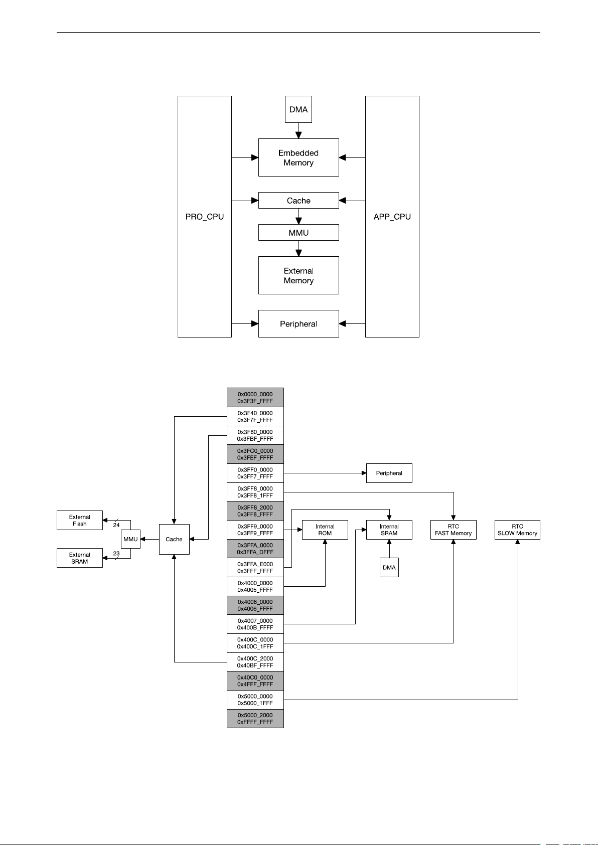
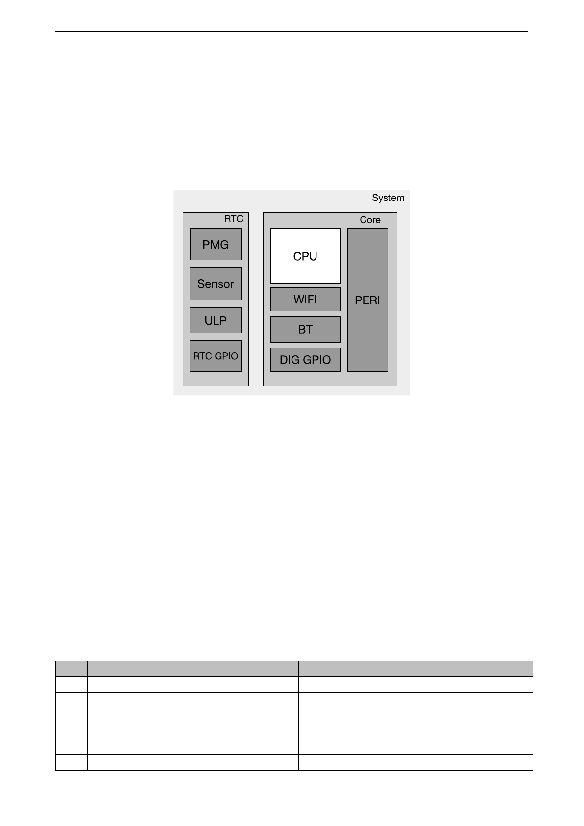
The ESP32 is a dual-core system with two Harvard Architecture Xtensa LX6 CPUs. All embedded memory,
external memory and peripherals are located on the data bus and/or the instruction bus of these CPUs.
With some minor exceptions (see below), the address mapping of two CPUs is symmetric, meaning they use the
same addresses to access the same memory. Multiple peripherals in the system can access embedded memory
via DMA.
The two CPUs are named “PRO_CPU” and “APP_CPU” (for “protocol” and “application”), however for most
purposes the two CPUs are interchangeable.
1.2 Features
• Address Space
– Symmetric address mapping
– 4 GB (32-bit) address space for both data bus and instruction bus
– 1296 KB embedded memory address space
– 19704 KB external memory address space
– 512 KB peripheral address space
– Some embedded and external memory regions can be accessed by either data bus or instruction bus
– 328 KB DMA address space
• Embedded Memory
– 448 KB Internal ROM
– 520 KB Internal SRAM
– 8 KB RTC FAST Memory
– 8 KB RTC SLOW Memory
• External Memory
Off-chip SPI memory can be mapped into the available address space as external memory. Parts of the
embedded memory can be used as transparent cache for this external memory.
– Supports up to 16 MB off-Chip SPI Flash.
– Supports up to 8 MB off-Chip SPI SRAM.
• Peripherals
– 41 peripherals
• DMA
– 13 modules are capable of DMA operation
Espressif Systems 8 ESP32 Technical Reference Manual V1.0
Page 10
1.2 Features 1 SYSTEM AND MEMORY
Figure 1 block diagram illustrates the system structure, the block diagram in Figure 2 illustrates the address map
structure.
Figure 1: System Structure
Figure 2: System Address Mapping
Espressif Systems 9 ESP32 Technical Reference Manual V1.0
Page 11

1.3 Functional Description 1 SYSTEM AND MEMORY
1.3 Functional Description
1.3.1 Address Mapping
Each of the two Harvard Architecture Xtensa LX6 CPUs has 4 GB (32-bit) address space. Address spaces are
symmetric between the two CPUs.
Addresses below 0x4000_0000 are serviced using the data bus. Addresses in the range 0x4000_0000 ~
0x4FFF_FFFF are serviced using the instruction bus. Finally, addresses over and including 0x5000_0000 are
shared by the data and instruction bus.
The data bus and instruction bus are both little-endian: for example, byte addresses 0x0, 0x1, 0x2, 0x3 access
the least significant, second least significant, second most significant, and most significant bytes of the 32-bit
word stored at address 0x0, respectively. The CPU can access data bus addresses via aligned or non-aligned
byte, half-word and word read and write operations. The CPU can read and write data through the instruction
bus, but only in a word aligned manner; non-word-aligned access will cause a CPU exception.
Each CPU can directly access embedded memory through both the data bus and the instruction bus, external
memory which is mapped into the address space (via transparent caching & MMU) and peripherals. Table 1
illustrates address ranges that can be accessed by each CPU’s data bus and instruction bus.
Some embedded memories and some external memories can be accessed via the data bus or the instruction
bus. In these cases, the same memory is available to either of the CPUs at two address ranges.
Table 1: Address Mapping
Bus Type
Data 0x3F40_0000 0x3F7F_FFFF 4 MB External Memory
Data 0x3F80_0000 0x3FBF_FFFF 4 MB External Memory
Data 0x3FF0_0000 0x3FF7_FFFF 512 KB Peripheral
Data 0x3FF8_0000 0x3FFF_FFFF 512 KB Embedded Memory
Instruction 0x4000_0000 0x400C_1FFF 776 KB Embedded Memory
Instruction 0x400C_2000 0x40BF_FFFF 11512 KB External Memory
Data Instruction 0x5000_0000 0x5000_1FFF 8 KB Embedded Memory
Low Address High Address
0x0000_0000 0x3F3F_FFFF Reserved
0x3FC0_0000 0x3FEF_FFFF 3 MB Reserved
0x40C0_0000 0x4FFF_FFFF 244 MB Reserved
0x5000_2000 0xFFFF_FFFF Reserved
Boundary Address
Size Target
1.3.2 Embedded Memory
The Embedded Memory consists of four segments: internal ROM (448 KB), internal SRAM (520 KB), RTC FAST
memory (8 KB) and RTC SLOW memory (8 KB).
The 448 KB internal ROM is divided into two parts: Internal ROM 0 (384 KB) and Internal ROM 1 (64 KB).
The 520 KB internal SRAM is divided into three parts: Internal SRAM 0 (192 KB), Internal SRAM 1 (128 KB), and
Internal SRAM 2 (200 KB).
RTC FAST Memory and RTC SLOW Memory are both implemented as SRAM.
Table 2 lists all embedded memories and their address ranges on the data and instruction buses.
Espressif Systems 10 ESP32 Technical Reference Manual V1.0
Page 12

1.3 Functional Description 1 SYSTEM AND MEMORY
Table 2: Embedded Memory Address Mapping
Bus Type
Data 0x3FF8_0000 0x3FF8_1FFF 8 KB RTC FAST Memory PRO_CPU Only
Data 0x3FF9_0000 0x3FF9_FFFF 64 KB Internal ROM 1 -
Data 0x3FFA_E000 0x3FFD_FFFF 200 KB Internal SRAM 2 DMA
Data 0x3FFE_0000 0x3FFF_FFFF 128 KB Internal SRAM 1 DMA
Bus Type
Instruction 0x4000_0000 0x4000_7FFF 32 KB Internal ROM 0 Remap
Instruction 0x4000_8000 0x4005_FFFF 352 KB Internal ROM 0 -
Instruction 0x4007_0000 0x4007_FFFF 64 KB Internal SRAM 0 Cache
Instruction 0x4008_0000 0x4009_FFFF 128 KB Internal SRAM 0 -
Instruction 0x400A_0000 0x400A_FFFF 64 KB Internal SRAM 1 -
Instruction 0x400B_0000 0x400B_7FFF 32 KB Internal SRAM 1 Remap
Instruction 0x400B_8000 0x400B_FFFF 32 KB Internal SRAM 1 -
Instruction 0x400C_0000 0x400C_1FFF 8 KB RTC FAST Memory PRO_CPU Only
Bus Type
Data Instruc-
tion
Low Address High Address
0x3FF8_2000 0x3FF8_FFFF 56 KB Reserved -
0x3FFA_0000 0x3FFA_DFFF 56 KB Reserved -
Low Address High Address
0x4006_0000 0x4006_FFFF 64 KB Reserved -
Low Address High Address
0x5000_0000 0x5000_1FFF 8 KB RTC SLOW Memory -
Boundary Address
Boundary Address
Boundary Address
Size Target Comment
Size Target Comment
Size Target Comment
1.3.2.1 Internal ROM 0
The capacity of Internal ROM 0 is 384 KB, It is accessible by both CPUs through the address range
0x4000_0000 ~ 0x4005_FFFF, which is on the instruction bus.
The address range of the first 32 KB of the ROM 0 (0x4000_0000 ~ 0x4000_7FFF) can be re-mapped to access
a part of Internal SRAM 1 that normally resides in the memory range 0x400B_0000 ~ 0x400B_7FFF instead.
While remapping, such 32 KB SRAM can not be accessed by address range 0x400B_0000 ~ 0x400B_7FFF any
more, but it can still be accessible through the data bus (0x3FFE_8000 ~ 0x3FFE_FFFF). This can be done on a
per-CPU basis: setting bit 0 of register DPORT_PRO_BOOT_REMAP_CTRL_REG or
DPORT_APP_BOOT_REMAP_CTRL_REG will remap SRAM for the PRO_CPU and APP_CPU,
respectively.
1.3.2.2 Internal ROM 1
The capacity of Internal ROM 1 is 64 KB. It can be read by either CPU at address range 0x3FF9_0000 ~
0x3FF9_FFFF of the data bus.
Espressif Systems 11 ESP32 Technical Reference Manual V1.0
Page 13

1.3 Functional Description 1 SYSTEM AND MEMORY
1.3.2.3 Internal SRAM 0
The capacity of Internal SRAM 0 is 192 KB. Hardware can be configured to use the first 64KB to cache external
memory access. When not used as cache, the first 64KB can be read and written by either CPU at addresses
0x4007_0000 ~ 0x4007_7FFF of the instruction bus. The remaining 128 KB can always be read and written by
either CPU at addresses 0x4007_8000 ~ 0x4007_FFFF of instruction bus.
1.3.2.4 Internal SRAM 1
The capacity of Internal SRAM 1 is 128 KB. Either CPU can read and write this memory at addresses
0x3FFE_0000 ~ 0x3FFF_FFFF of the data bus, and also at addresses 0x400A_0000 ~ 0x400B_FFFF of the
instruction bus.
The address range accessed via the instruction bus is in reverse order (word-wise) compared to access via the
data bus. That is to say, address
0x3FFE_0000 and 0x400B_FFFC access the same word
0x3FFE_0004 and 0x400B_FFF8 access the same word
0x3FFE_0008 and 0x400B_FFF4 access the same word
……
0x3FFF_FFF4 and 0x400A_0008 access the same word
0x3FFF_FFF8 and 0x400A_0004 access the same word
0x3FFF_FFFC and 0x400A_0000 access the same word
The data bus and instruction bus of the CPU are still both little endian, so the byte order of individual words is not
reversed between address spaces. For example, address
0x3FFE_0000 accesses the least significant byte in the word accessed by 0x400B_FFFC.
0x3FFE_0001 accesses the second least significant byte in the word accessed by 0x400B_FFFC.
0x3FFE_0002 accesses the second most significant byte in the word accessed by 0x400B_FFFC.
0x3FFE_0003 accesses the most significant byte in the word accessed by 0x400B_FFFC.
0x3FFE_0004 accesses the least significant byte in the word accessed by 0x400B_FFF8.
0x3FFE_0005 accesses the second least significant byte in the word accessed by 0x400B_FFF8.
0x3FFE_0006 accesses the second most significant byte in the word accessed by 0x400B_FFF8.
0x3FFE_0007 accesses the most significant byte in the word accessed by 0x400B_FFF8.
……
0x3FFF_FFF8 accesses the least significant byte in the word accessed by 0x400A_0004.
0x3FFF_FFF9 accesses the second least significant byte in the word accessed by 0x400A_0004.
0x3FFF_FFFA accesses the second most significant byte in the word accessed by 0x400A_0004.
0x3FFF_FFFB accesses the most significant byte in the word accessed by 0x400A_0004.
0x3FFF_FFFC accesses the least significant byte in the word accessed by 0x400A_0000.
0x3FFF_FFFD accesses the second most significant byte in the word accessed by 0x400A_0000.
0x3FFF_FFFE accesses the second most significant byte in the word accessed by 0x400A_0000.
0x3FFF_FFFF accesses the most significant byte in the word accessed by 0x400A_0000.
Part of this memory can be remapped to the ROM 0 address space. See Internal Rom 0 for more
information.
Espressif Systems 12 ESP32 Technical Reference Manual V1.0
Page 14

1.3 Functional Description 1 SYSTEM AND MEMORY
1.3.2.5 Internal SRAM 2
The capacity of Internal SRAM 2 is 200 KB. It can be read and written by either CPU at addresses 0x3FFA_E000
~ 0x3FFD_FFFF on the data bus.
1.3.2.6 DMA
DMA uses the same addressing as the CPU data bus to read and write Internal SRAM 1 and Internal SRAM 2.
This means DMA uses address range 0x3FFE_0000 ~ 0x3FFF_FFFF to read and write Internal SRAM 1 and
address range 0x3FFA_E000 ~ 0x3FFD_FFFF to read and write Internal SRAM 2.
In the ESP32, 13 peripherals are equipped with DMA. Table 3 lists these peripherals.
Table 3: Module with DMA
UART0 UART1 UART2
SPI1 SPI2 SPI3
I2S0 I2S1
SDIO Slave SDMMC
EMAC
BT WIFI
1.3.2.7 RTC FAST Memory
RTC FAST Memory is 8 KB of SRAM. It can be read and written by PRO_CPU only at address range
0x3FF8_0000 ~ 0x3FF8_1FFF on the data bus or address range 0x400C_0000 ~ 0x400C_1FFF on the
instruction bus. Unlike most other memory regions, RTC FAST memory cannot be accessed by the
APP_CPU.
The two address ranges of PRO_CPU access RTC FAST Memory in the same order, so for example, address
0x3FF8_0000 and 0x400C_0000 access the same word. On the APP_CPU, these address ranges do not
provide access to RTC FAST Memory or any other memory location.
1.3.2.8 RTC SLOW Memory
RTC SLOW Memory is 8 KB of SRAM which can be read from and written by either CPU at address range
0x5000_0000 ~ 0x5000_1FFF. This address range is shared by both the data bus and the instruction bus.
1.3.3 External Memory
The ESP32 can access external SPI flash and SPI SRAM as external memory. Table 4 provides a list of external
memories that can be accessed by either CPU at a range of addresses on the data and instruction buses. When
a CPU accesses external memory through the Cache and MMU, the cache will map the CPU’s address to an
external physical memory address (in the external memory’s address space), according to the MMU settings. Due
to this address mapping, the ESP32 can address up to 16 MB External Flash and 8 MB External SRAM.
Espressif Systems 13 ESP32 Technical Reference Manual V1.0
Page 15

1.3 Functional Description 1 SYSTEM AND MEMORY
Table 4: External Memory Address Mapping
Bus Type
Data 0x3F40_0000 0x3F7F_FFFF 4 MB External Flash Read
Data 0x3F80_0000 0x3FBF_FFFF 4 MB External SRAM Read and Write
Bus Type
Instruction 0x400C_2000 0x40BF_FFFF 11512 KB External Flash Read
Low Address High Address
Low Address High Address
Boundary Address
Boundary Address
Size Target Comment
Size Target Comment
1.3.4 Peripherals
The ESP32 has 41 peripherals. Table 5 specifically describes the peripherals their respective address ranges.
Almost all peripheral modules can be accessed by either CPU at the same address, the only exception being the
PID Controller.
Table 5: Peripheral Address Mapping
Bus Type
Data 0x3FF0_0000 0x3FF0_0FFF 4 KB DPort Register
Data 0x3FF0_1000 0x3FF0_1FFF 4 KB AES Accelerator
Data 0x3FF0_2000 0x3FF0_2FFF 4 KB RSA Accelerator
Data 0x3FF0_3000 0x3FF0_3FFF 4 KB SHA Accelerator
Data 0x3FF0_4000 0x3FF0_4FFF 4 KB Secure Boot
Data 0x3FF1_0000 0x3FF1_3FFF 16 KB Cache MMU Table
Data 0x3FF1_F000 0x3FF1_FFFF 4 KB PID Controller Per-CPU peripheral
Data 0x3FF4_0000 0x3FF4_0FFF 4 KB UART0
Data 0x3FF4_2000 0x3FF4_2FFF 4 KB SPI1
Data 0x3FF4_3000 0x3FF4_3FFF 4 KB SPI0
Data 0x3FF4_4000 0x3FF4_4FFF 4 KB GPIO
Data 0x3FF4_8000 0x3FF4_8FFF 4 KB RTC
Data 0x3FF4_9000 0x3FF4_9FFF 4 KB IO MUX
Data 0x3FF4_B000 0x3FF4_BFFF 4 KB SDIO Slave One of three parts
Data 0x3FF4_C000 0x3FF4_CFFF 4 KB UDMA1
Data 0x3FF4_F000 0x3FF4_FFFF 4 KB I2S0
Data 0x3FF5_0000 0x3FF5_0FFF 4 KB UART1
Data 0x3FF5_3000 0x3FF5_3FFF 4 KB I2C0
Data 0x3FF5_4000 0x3FF5_4FFF 4 KB UDMA0
Low Address High Address
0x3FF0_5000 0x3FF0_FFFF 44 KB Reserved
0x3FF1_4000 0x3FF1_EFFF 44 KB Reserved
0x3FF2_0000 0x3FF3_FFFF 128 KB Reserved
0x3FF4_1000 0x3FF4_1FFF 4 KB Reserved
0x3FF4_5000 0x3FF4_7FFF 12 KB Reserved
0x3FF4_A000 0x3FF4_AFFF 4 KB Reserved
0x3FF4_D000 0x3FF4_EFFF 8 KB Reserved
0x3FF5_1000 0x3FF5_2FFF 8 KB Reserved
Boundary Address
Size Target Comment
Espressif Systems 14 ESP32 Technical Reference Manual V1.0
Page 16

1.3 Functional Description 1 SYSTEM AND MEMORY
Bus Type
Data 0x3FF5_5000 0x3FF5_5FFF 4 KB SDIO Slave One of three parts
Data 0x3FF5_6000 0x3FF5_6FFF 4 KB RMT
Data 0x3FF5_7000 0x3FF5_7FFF 4 KB PCNT
Data 0x3FF5_8000 0x3FF5_8FFF 4 KB SDIO Slave One of three parts
Data 0x3FF5_9000 0x3FF5_9FFF 4 KB LED PWM
Data 0x3FF5_A000 0x3FF5_AFFF 4 KB Efuse Controller
Data 0x3FF5_B000 0x3FF5_BFFF 4 KB Flash Encryption
Data 0x3FF5_E000 0x3FF5_EFFF 4 KB PWM0
Data 0x3FF5_F000 0x3FF5_FFFF 4 KB TIMG0
Data 0x3FF6_0000 0x3FF6_0FFF 4 KB TIMG1
Data 0x3FF6_4000 0x3FF6_4FFF 4 KB SPI2
Data 0x3FF6_5000 0x3FF6_5FFF 4 KB SPI3
Data 0x3FF6_6000 0x3FF6_6FFF 4 KB SYSCON
Data 0x3FF6_7000 0x3FF6_7FFF 4 KB I2C1
Data 0x3FF6_8000 0x3FF6_8FFF 4 KB SDMMC
Data 0x3FF6_9000 0x3FF6_AFFF 8 KB EMAC
Data 0x3FF6_C000 0x3FF6_CFFF 4 KB PWM1
Data 0x3FF6_D000 0x3FF6_DFFF 4 KB I2S1
Data 0x3FF6_E000 0x3FF6_EFFF 4 KB UART2
Data 0x3FF6_F000 0x3FF6_FFFF 4 KB PWM2
Data 0x3FF7_0000 0x3FF7_0FFF 4 KB PWM3
Data 0x3FF7_5000 0x3FF7_5FFF 4 KB RNG
Low Address High Address
0x3FF5_C000 0x3FF5_DFFF 8 KB Reserved
0x3FF6_1000 0x3FF6_3FFF 12 KB Reserved
0x3FF6_B000 0x3FF6_BFFF 4 KB Reserved
0x3FF7_1000 0x3FF7_4FFF 16 KB Reserved
0x3FF7_6000 0x3FF7_FFFF 40 KB Reserved
Boundary Address
Size Target Comment
1.3.4.1 Asymmetric PID Controller Peripheral
There are two PID Controllers in the system. They serve the PRO_CPU and the APP_CPU, respectively. The
PRO_CPU and the APP_CPU can only access their own PID Controller and not their counterpart’s PID
Controller. Each CPU uses the same memory range 0x3FF1_F000 ~ 3FF1_FFFF to access its own PID
Controller.
1.3.4.2 Non-Contiguous Peripheral Memory Ranges
The SDIO Slave peripheral consists of three parts and the two CPUs use non-contiguous addresses to access
these. The three parts are accessed at the address ranges 0x3FF4_B000 ~ 3FF4_BFFF, 0x3FF5_5000 ~
3FF5_5FFF and 0x3FF5_8000 ~ 3FF5_8FFF of each CPU’s data bus. Similar to other peripherals, access to this
peripheral is identical for both CPUs.
Espressif Systems 15 ESP32 Technical Reference Manual V1.0
Page 17

1.3 Functional Description 1 SYSTEM AND MEMORY
1.3.4.3 Memory Speed
The ROM as well as the SRAM are both clocked from CPU_CLK and can be accessed by the CPU in a single
cycle. The RTC FAST memory is clocked from the APB_CLOCK and the RTC SLOW memory from the
FAST_CLOCK, so access to these memories may be slower. DMA uses the APB_CLK to access memory.
Internally, the SRAM is organized in 32K-sized banks. Each CPU and DMA channel can access the SRAM at full
speed and simultaneously, provided they access address different memory banks.
Espressif Systems 16 ESP32 Technical Reference Manual V1.0
Page 18
2 INTERRUPT MATRIX
2. Interrupt Matrix
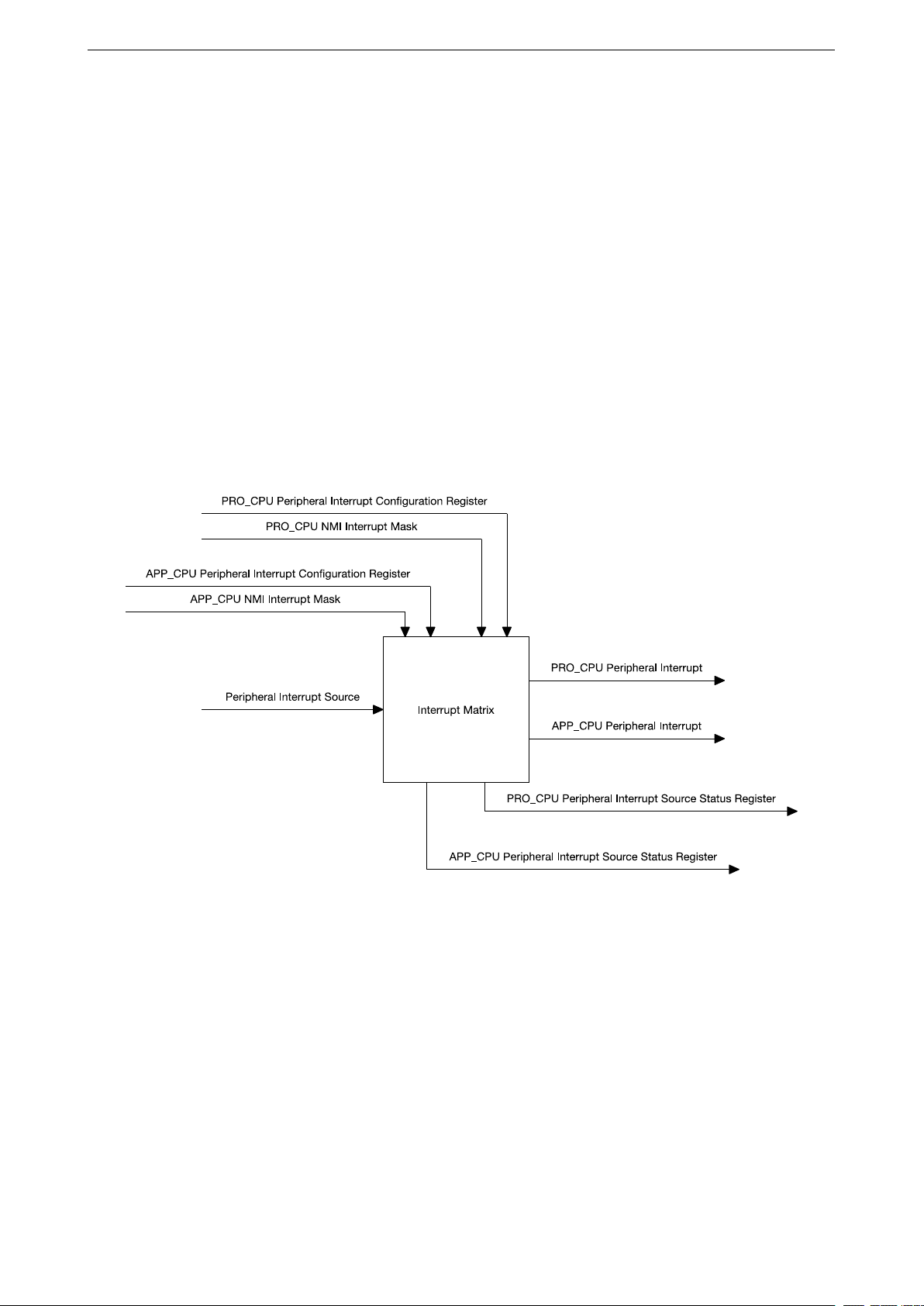
2.1 Introduction
The Interrupt Matrix embedded in the ESP32 independently allocates peripheral interrupt sources to the two
CPUs’ peripheral interrupts. This configuration is highly flexible in order to meet many different needs.
2.2 Features
• Accepts 71 peripheral interrupt sources as input.
• Generates 26 peripheral interrupt sources per CPU as output (52 total).
• CPU NMI Interrupt Mask.
• Queries current interrupt status of peripheral interrupt sources.
The structure of the Interrupt Matrix is shown in Figure 3.
Figure 3: Interrupt Matrix Structure
2.3 Functional Description
2.3.1 Peripheral Interrupt Source
ESP32 has 71 peripheral interrupt sources in total. All peripheral interrupt sources are listed in table 6. 67 of 71
ESP32 peripheral interrupt sources can be allocated to either CPU.
The four remaining peripheral interrupt sources are CPU-specific, two per CPU. GPIO_INTERRUPT_PRO and
GPIO_INTERRUPT_PRO_NMI can only be allocated to PRO_CPU. GPIO_INTERRUPT_APP and
GPIO_INTERRUPT_APP_NMI can only be allocated to APP_CPU. As a result, PRO_CPU and APP_CPU each
have 69 peripheral interrupt sources.
Espressif Systems 17 ESP32 Technical Reference Manual V1.0
Page 19
Espressif Systems 18 ESP32 Technical Reference Manual V1.0
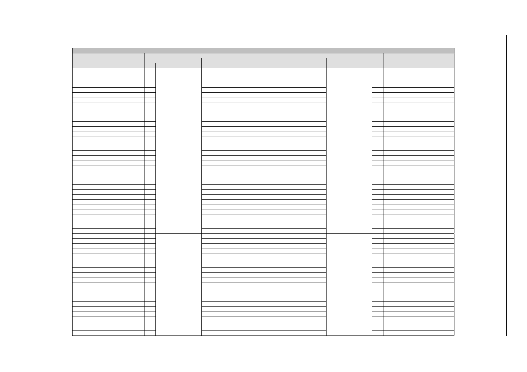
Table 6: PRO_CPU, APP_CPU interrupt configuration
2.3 Functional Description 2 INTERRUPT MATRIX
PRO_CPU APP_CPU
Peripheral Interrupt
Configuration Register
PRO_MAC_INTR_MAP_REG 0
PRO_MAC_NMI_MAP_REG 1 1 MAC_NMI 1 1 APP_MAC_NMI_MAP_REG
PRO_BB_INT_MAP_REG 2 2 BB_INT 2 2 APP_BB_INT_MAP_REG
PRO_BT_MAC_INT_MAP_REG 3 3 BT_MAC_INT 3 3 APP_BT_MAC_INT_MAP_REG
PRO_BT_BB_INT_MAP_REG 4 4 BT_BB_INT 4 4 APP_BT_BB_INT_MAP_REG
PRO_BT_BB_NMI_MAP_REG 5 5 BT_BB_NMI 5 5 APP_BT_BB_NMI_MAP_REG
PRO_RWBT_IRQ_MAP_REG 6 6 RWBT_IRQ 6 6 APP_RWBT_IRQ_MAP_REG
PRO_BT_BB_NMI_MAP_REG 5 5 BT_BB_NMI 5 5 APP_BT_BB_NMI_MAP_REG
PRO_RWBT_IRQ_MAP_REG 6 6 RWBT_IRQ 6 6 APP_RWBT_IRQ_MAP_REG
PRO_RWBLE_IRQ_MAP_REG 7 7 RWBLE_IRQ 7 7 APP_RWBLE_IRQ_MAP_REG
PRO_RWBT_NMI_MAP_REG 8 8 RWBT_NMI 8 8 APP_RWBT_NMI_MAP_REG
PRO_RWBLE_NMI_MAP_REG 9 9 RWBLE_NMI 9 9 APP_RWBLE_NMI_MAP_REG
PRO_SLC0_INTR_MAP_REG 10 10 SLC0_INTR 10 10 APP_SLC0_INTR_MAP_REG
PRO_SLC1_INTR_MAP_REG 11 11 SLC1_INTR 11 11 APP_SLC1_INTR_MAP_REG
PRO_UHCI0_INTR_MAP_REG 12 12 UHCI0_INTR 12 12 APP_UHCI0_INTR_MAP_REG
PRO_UHCI1_INTR_MAP_REG 13 13 UHCI1_INTR 13 13 APP_UHCI1_INTR_MAP_REG
PRO_TG_T0_LEVEL_INT_MAP_REG 14 14 TG_T0_LEVEL_INT 14 14 APP_TG_T0_LEVEL_INT_MAP_REG
PRO_TG_T1_LEVEL_INT_MAP_REG 15 15 TG_T1_LEVEL_INT 15 15 APP_TG_T1_LEVEL_INT_MAP_REG
PRO_TG_WDT_LEVEL_INT_MAP_REG 16 16 TG_WDT_LEVEL_INT 16 16 APP_TG_WDT_LEVEL_INT_MAP_REG
PRO_TG_LACT_LEVEL_INT_MAP_REG 17 17 TG_LACT_LEVEL_INT 17 17 APP_TG_LACT_LEVEL_INT_MAP_REG
PRO_TG1_T0_LEVEL_INT_MAP_REG 18 18 TG1_T0_LEVEL_INT 18 18 APP_TG1_T0_LEVEL_INT_MAP_REG
PRO_TG1_T1_LEVEL_INT_MAP_REG 19 19 TG1_T1_LEVEL_INT 19 19 APP_TG1_T1_LEVEL_INT_MAP_REG
PRO_TG1_WDT_LEVEL_INT_MAP_REG 20 20 TG1_WDT_LEVEL_INT 20 20 APP_TG1_WDT_LEVEL_INT_MAP_REG
PRO_TG1_LACT_LEVEL_INT_MAP_REG 21 21 TG1_LACT_LEVEL_INT 21 21 APP_TG1_LACT_LEVEL_INT_MAP_REG
PRO_GPIO_INTERRUPT_PRO_MAP_REG
PRO_GPIO_INTERRUPT_PRO_NMI_MAP_REG
PRO_CPU_INTR_FROM_CPU_0_MAP_REG 24 24 CPU_INTR_FROM_CPU_0 24 24 APP_CPU_INTR_FROM_CPU_0_MAP_REG
PRO_CPU_INTR_FROM_CPU_1_MAP_REG 25 25 CPU_INTR_FROM_CPU_1 25 25 APP_CPU_INTR_FROM_CPU_1_MAP_REG
PRO_CPU_INTR_FROM_CPU_2_MAP_REG 26 26 CPU_INTR_FROM_CPU_2 26 26 APP_CPU_INTR_FROM_CPU_2_MAP_REG
PRO_CPU_INTR_FROM_CPU_3_MAP_REG 27 27 CPU_INTR_FROM_CPU_3 27 27 APP_CPU_INTR_FROM_CPU_3_MAP_REG
PRO_SPI_INTR_0_MAP_REG 28 28 SPI_INTR_0 28 28 APP_SPI_INTR_0_MAP_REG
PRO_SPI_INTR_1_MAP_REG 29 29 SPI_INTR_1 29 29 APP_SPI_INTR_1_MAP_REG
PRO_SPI_INTR_2_MAP_REG 30 30 SPI_INTR_2 30 30 APP_SPI_INTR_2_MAP_REG
PRO_SPI_INTR_3_MAP_REG 31 31 SPI_INTR_3 31 31 APP_SPI_INTR_3_MAP_REG
PRO_I2S0_INT_MAP_REG 0
PRO_I2S1_INT_MAP_REG 1 33 I2S1_INT 33 1 APP_I2S1_INT_MAP_REG
PRO_UART_INTR_MAP_REG 2 34 UART_INTR 34 2 APP_UAR T_INTR_MAP_REG
PRO_UART1_INTR_MAP_REG 3 35 UART1_INTR 35 3 APP_UART1_INTR_MAP_REG
PRO_UART2_INTR_MAP_REG 4 36 UART2_INTR 36 4 APP_UART2_INTR_MAP_REG
PRO_SDIO_HOST_INTERRUPT_MAP_REG 5 37 SDIO_HOST_INTERRUPT 37 5 APP_SDIO_HOST_INTERRUPT_MAP_REG
PRO_EMAC_INT_MAP_REG 6 38 EMAC_INT 38 6 APP_EMAC_INT_MAP_REG
PRO_PWM0_INTR_MAP_REG 7 39 PWM0_INTR 39 7 APP_PWM0_INTR_MAP_REG
PRO_PWM1_INTR_MAP_REG 8 40 PWM1_INTR 40 8 APP_PWM1_INTR_MAP_REG
PRO_PWM2_INTR_MAP_REG 9 41 PWM2_INTR 41 9 APP_PWM2_INTR_MAP_REG
PRO_PWM3_INTR_MAP_REG 10 42 PWM3_INTR 42 10 APP_PWM3_INTR_MAP_REG
PRO_LEDC_INT_MAP_REG 11 43 LEDC_INT 43 11 APP_LEDC_INT_MAP_REG
PRO_EFUSE_INT_MAP_REG 12 44 EFUSE_INT 44 12 APP_EFUSE_INT_MAP_REG
PRO_CAN_INT_MAP_REG 13 45 CAN_INT 45 13 APP_CAN_INT_MAP_REG
PRO_RTC_CORE_INTR_MAP_REG 14 46 RTC_CORE_INTR 46 14 APP_R TC_CORE_INTR_MAP_REG
PRO_RMT_INTR_MAP_REG 15 47 RMT_INTR 47 15 APP_RMT_INTR_MAP_REG
PRO_PCNT_INTR_MAP_REG 16 48 PCNT_INTR 48 16 APP_PCNT_INTR_MAP_REG
PRO_I2C_EXT0_INTR_MAP_REG 17 49 I2C_EXT0_INTR 49 17 APP_I2C_EXT0_INTR_MAP_REG
PRO_I2C_EXT1_INTR_MAP_REG 18 50 I2C_EXT1_INTR 50 18 APP_I2C_EXT1_INTR_MAP_REG
PRO_RSA_INTR_MAP_REG 19 51 RSA_INTR 51 19 APP_RSA_INTR_MAP_REG
PRO_SPI1_DMA_INT_MAP_REG 20 52 SPI1_DMA_INT 52 20 APP_SPI1_DMA_INT_MAP_REG
Status Register Status Register
Bit Name
PRO_INTR_STATUS_REG_0
22 22
23 23
PRO_INTR_STATUS_REG_1
No. Name No.
0 MAC_INTR 0
GPIO_INTERRUPT_PRO GPIO_INTERRUPT_APP
GPIO_INTERRUPT_PRO_NMI GPIO_INTERRUPT_APP_NMI
32 I2S0_INT 32
Peripheral Interrupt Source
Name Bit
APP_INTR_STATUS_REG_0
22 22
23 23
APP_INTR_STATUS_REG_1
Peripheral Interrupt
Configuration Register
0 APP_MAC_INTR_MAP_REG
APP_GPIO_INTERRUPT_APP_MAP_REG
APP_GPIO_INTERRUPT_APP_NMI_MAP_REG
0 APP_I2S0_INT_MAP_REG
Page 20
Espressif Systems 19 ESP32 Technical Reference Manual V1.0
PRO_CPU APP_CPU
Peripheral Interrupt
Configuration Register
PRO_SPI2_DMA_INT_MAP_REG 21
PRO_SPI3_DMA_INT_MAP_REG 22 54 SPI3_DMA_INT 54 22 APP_SPI3_DMA_INT_MAP_REG
PRO_WDG_INT_MAP_REG 23 55 WDG_INT 55 23 APP_WDG_INT_MAP_REG
PRO_TIMER_INT1_MAP_REG 24 56 TIMER_INT1 56 24 APP_TIMER_INT1_MAP_REG
PRO_TIMER_INT2_MAP_REG 25 57 TIMER_INT2 57 25 APP_TIMER_INT2_MAP_REG
PRO_TG_T0_EDGE_INT_MAP_REG 26 58 TG_T0_EDGE_INT 58 26 APP_TG_T0_EDGE_INT_MAP_REG
PRO_TG_T1_EDGE_INT_MAP_REG 27 59 TG_T1_EDGE_INT 59 27 APP_TG_T1_EDGE_INT_MAP_REG
PRO_TG_WDT_EDGE_INT_MAP_REG 28 60 TG_WDT_EDGE_INT 60 28 APP_TG_WDT_EDGE_INT_MAP_REG
PRO_TG_LACT_EDGE_INT_MAP_REG 29 61 TG_LACT_EDGE_INT 61 29 APP_TG_LACT_EDGE_INT_MAP_REG
PRO_TG1_T0_EDGE_INT_MAP_REG 30 62 TG1_T0_EDGE_INT 62 30 APP_TG1_T0_EDGE_INT_MAP_REG
PRO_TG1_T1_EDGE_INT_MAP_REG 31 63 TG1_T1_EDGE_INT 63 31 APP_TG1_T1_EDGE_INT_MAP_REG
PRO_TG1_WDT_EDGE_INT_MAP_REG 0
PRO_TG1_LACT_EDGE_INT_MAP_REG 1 65 TG1_LACT_EDGE_INT 65 1 APP_TG1_LACT_EDGE_INT_MAP_REG
PRO_MMU_IA_INT_MAP_REG 2 66 MMU_IA_INT 66 2 APP_MMU_IA_INT_MAP_REG
PRO_MPU_IA_INT_MAP_REG 3 67 MPU_IA_INT 67 3 APP_MPU_IA_INT_MAP_REG
PRO_CACHE_IA_INT_MAP_REG 4 68 CACHE_IA_INT 68 4 APP_CACHE_IA_INT_MAP_REG
Status Register Status Register
Bit Name
PRO_INTR_STATUS_REG_1
PRO_INTR_STATUS_REG_2
No. Name No.
53 SPI2_DMA_INT 53
64 TG1_WDT_EDGE_INT 64
Peripheral Interrupt Source
Name Bit
APP_INTR_STATUS_REG_1
APP_INTR_STATUS_REG_2
Peripheral Interrupt
Configuration Register
21 APP_SPI2_DMA_INT_MAP_REG
0 APP_TG1_WDT_EDGE_INT_MAP_REG
2.3 Functional Description 2 INTERRUPT MATRIX
Page 21

2.3 Functional Description 2 INTERRUPT MATRIX
2.3.2 CPU Interrupt
Both of the two CPUs (PRO and APP) have 32 interrupts each, of which 26 are peripheral interrupts. All
interrupts in a CPU are listed in Table 7.
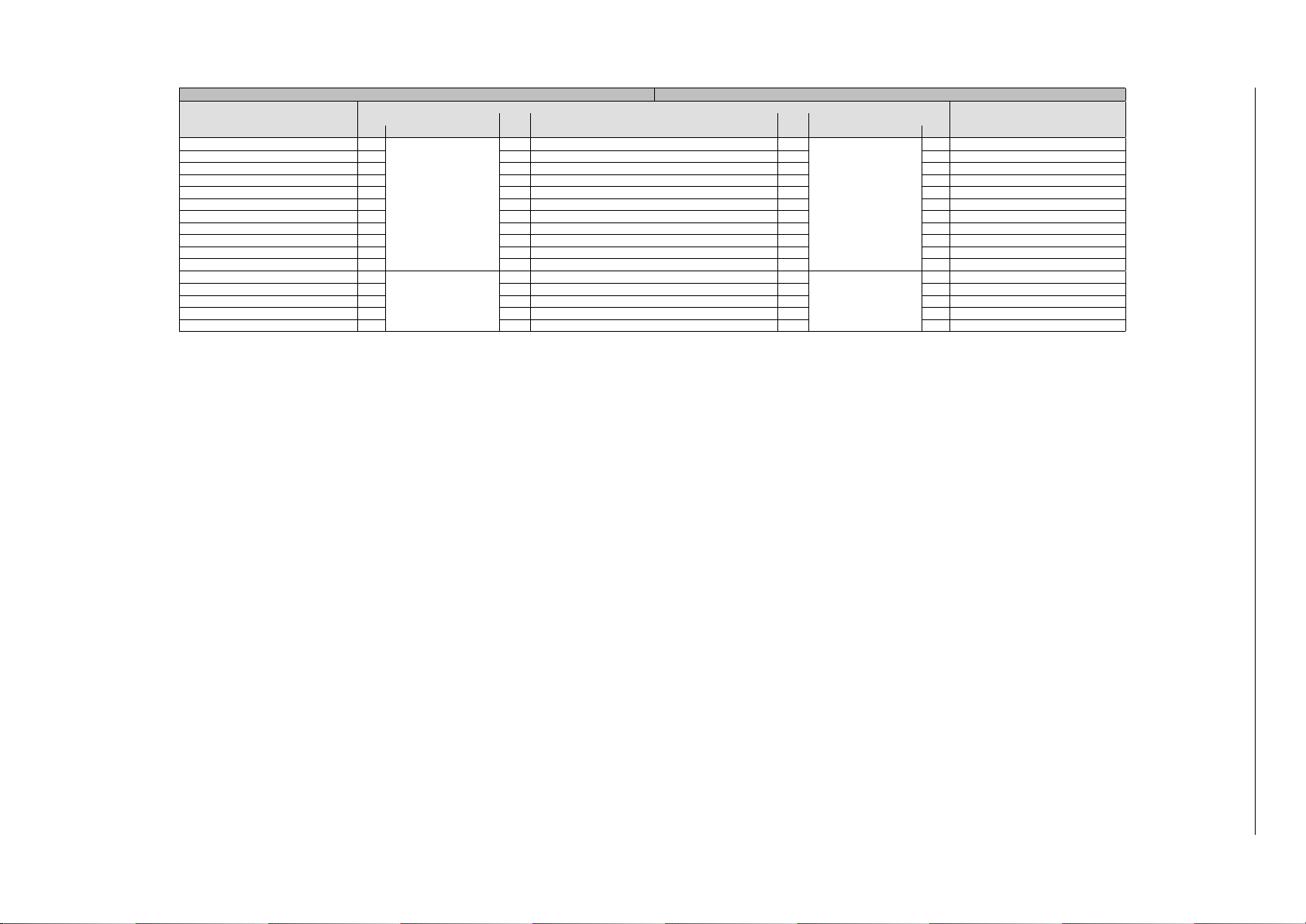
Table 7: CPU Interrupts
No. Category Type Priority Level
0 Peripheral Level-Triggered 1
1 Peripheral Level-Triggered 1
2 Peripheral Level-Triggered 1
3 Peripheral Level-Triggered 1
4 Peripheral Level-Triggered 1
5 Peripheral Level-Triggered 1
6 Internal Timer.0 1
7 Internal Software 1
8 Peripheral Level-Triggered 1
9 Peripheral Level-Triggered 1
10 Peripheral Edge-Triggered 1
11 Internal Profiling 3
12 Peripheral Level-Triggered 1
13 Peripheral Level-Triggered 1
14 Peripheral NMI NMI
15 Internal Timer.1 3
16 Internal Timer.2 5
17 Peripheral Level-Triggered 1
18 Peripheral Level-Triggered 1
19 Peripheral Level-Triggered 2
20 Peripheral Level-Triggered 2
21 Peripheral Level-Triggered 2
22 Peripheral Edge-Triggered 3
23 Peripheral Level-Triggered 3
24 Peripheral Level-Triggered 4
25 Peripheral Level-Triggered 4
26 Peripheral Level-Triggered 5
27 Peripheral Level-Triggered 3
28 Peripheral Edge-Triggered 4
29 Internal Software 3
30 Peripheral Edge-Triggered 4
31 Peripheral Level-Triggered 5
2.3.3 Allocate Peripheral Interrupt Sources to Peripheral Interrupt on CPU
In this section:
• Source_X stands for any particular peripheral interrupt source.
• PRO_X_MAP_REG (or APP_X_MAP_REG) stands for any particular peripheral interrupt configuration
Espressif Systems 20 ESP32 Technical Reference Manual V1.0
Page 22

2.3 Functional Description 2 INTERRUPT MATRIX
register of the PRO_CPU (or APP_CPU). The peripheral interrupt configuration register corresponds to the
peripheral interrupt source Source_X. Referring to Table 6, the registers listed under “PRO_CPU
(APP_CPU) - Peripheral Interrupt Configuration Register” correspond to the peripheral interrupt sources
listed in “Peripheral Interrupt Source - Name”.
• Interrupt_P stands for CPU peripheral interrupt, numbered as Num_P. Num_P can take the ranges 0 ~ 5, 8
~ 10, 12 ~ 14, 17 ~ 28, 30 ~ 31.
• Interrupt_I stands for CPU internal interrupt numbered as Num_I. Num_I can take values 6, 7, 11, 15, 16,
29.
Using this terminology, the possible operations of the Interrupt Matrix controller can be described as
follows:
• Allocate peripheral interrupt source Source_X to CPU (PRO_CPU or APP_CPU)
Set PRO_X_MAP_REG�or APP_X_MAP_REG�to Num_P. Num_P can be any CPU peripheral interrupt
number. CPU interrupts can be shared between multiple peripherals (see below).
• Disable peripheral interrupt source Source_X for CPU (PRO_CPU or APP_CPU)
Set PRO_X_MAP_REG�or APP_X _MAP_REG�for peripheral interrupt source to any Num_I. The specific
choice of internal interrupt number does not change behaviour, as none of the interrupt numbered as
Num_I are connected to either CPU.
• Allocate multiple peripheral sources Source_Xn ORed to PRO_CPU (APP_CPU) peripheral interrupt
Set multiple PRO_Xn_MAP_REG (APP_Xn_MAP_REG) to the same Num_P. Any of these peripheral
interrupts will trigger CPU Interrupt_P.
2.3.4 CPU NMI Interrupt Mask
The Interrupt Matrix temporarily masks all peripheral interrupt sources allocated to PRO_CPU’s ( or APP_CPU’s )
NMI interrupt if it receives the signal PRO_CPU NMI Interrupt Mask ( or APP_CPU NMI Interrupt Mask ) from the
peripheral PID Controller respectively.
2.3.5 Query Current Interrupt Status of Peripheral Interrupt Source
The current interrupt status of a peripheral interrupt source can be read via the bit value in
PRO_INTR_STATUS_REG_n (APP_INTR_STATUS_REG_n) as shown in the mapping in Table 6.
Espressif Systems 21 ESP32 Technical Reference Manual V1.0
Page 23
3 RESET AND CLOCK
3. Reset and Clock
3.1 System Reset
3.1.1 Introduction
The ESP32 has three reset levels: CPU reset, Core reset, and System reset. None of these reset levels clear the
RAM. Figure 4 shows the subsystems included in each reset level.
Figure 4: System Reset
• CPU reset: Only resets the registers of one or both the CPU cores.
• Core reset: Resets all the digital registers, including CPU cores, external GPIO and digital GPIO. The RTC is
not reset.
• System reset: Resets all the registers on the chip, including those of the RTC.
3.1.2 Reset Source
While most of the time the APP_CPU and PRO_CPU will be reset simultaneously, some reset sources are able to
reset only one of the two cores. The reset reason for each core can be looked up individually: the PRO_CPU
reset reason will be stored in RTC_CNTL_RESET_CAUSE_PROCPU, the reset reason for the APP_CPU in
APP_CNTL_RESET_CAUSE_PROCPU. Table 8 shows the possible reset reason values that can be read from
these registers.
Table 8: PRO_CPU and APP_CPU reset reason values
PRO APP Source Reset Type Note
0x01 0x01 Chip Power On Reset System Reset -
0x10 0x10 RWDT System Reset System Reset Refer to WDT Chapter.
0x0F 0x0F Brown Out Reset System Reset Refer to Power Management Chapter.
0x03 0x03 Software System Reset Core Reset Configure RTC_CNTL_SW_SYS_RST register.
0x05 0x05 Deep Sleep Rest Core Reset Refer to Power Management Chapter.
0x07 0x07 MWDT0 Global Reset Core Reset Refer to WDT Chapter.
Espressif Systems 22 ESP32 Technical Reference Manual V1.0
Page 24
3.2 System Clock 3 RESET AND CLOCK
PRO APP APP Source Reset Type Note
0x08 0x08 MWDT1 Global Reset Core Reset Refer to WDT Chapter.
0x09 0x09 RWDT Core Reset Core Reset Refer to WDT Chapter.
0x0B - MWDT0 CPU Reset CPU Reset Refer to WDT Chapter.
0x0C - Software CPU Reset CPU Reset Configure RTC_CNTL_SW_APPCPU_RST register.
- 0x0B MWDT1 CPU Reset CPU Reset Refer to WDT Chapter.
- 0x0C Software CPU Reset CPU Reset Configure RTC_CNTL_SW_APPCPU_RST register.
0x0D 0x0D RWDT CPU Reset CPU Reset Refer to WDT Chapter.
Indicates that the PRO CPU has indepen-
- 0xE PRO CPU Reset CPU Reset
dently reset the APP CPU by configuring the
DPORT_APPCPU_RESETTING register.
3.2 System Clock
3.2.1 Introduction
The ESP32 integrates multiple clock sources for the CPU cores, the peripherals and the RTC. These clocks can
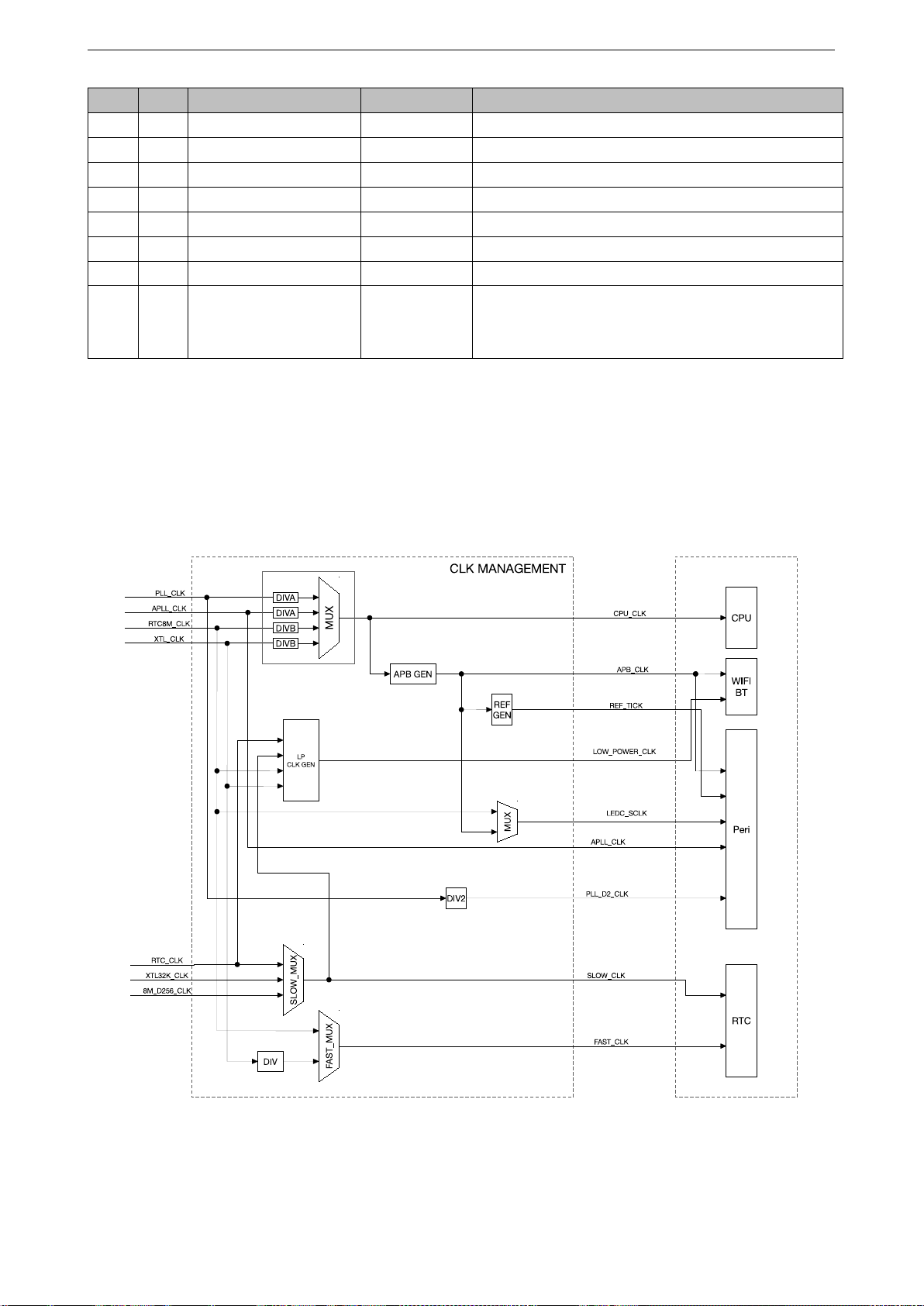
be configured to meet different requirements. Figure 5 shows the system clock structure.
Figure 5: System Clock
Espressif Systems 23 ESP32 Technical Reference Manual V1.0
Page 25

3.2 System Clock 3 RESET AND CLOCK
3.2.2 Clock Source
The ESP32 can use an external crystal oscillator, an internal PLL or an oscillating circuit as a clock source.
Specifically, the clock sources available are:
• High Speed Clocks
– PLL_CLK is an internal PLL clock with a frequency of 320 MHz.
– XTL_CLK is a clock signal generated using an external crystal with a frequency range of 2 ~ 40 MHz.
• Low Power Clocks
– XTL32K_CLK is a clock generated using an external crystal with a frequency of 32 KHz.
– RTC8M_CLK is an internal clock with a default frequency of 8 MHz. This frequency is adjustable.
– RTC8M_D256_CLK is divided from RTC8M_CLK 256. Its frequency is (RTC8M_CLK / 256). With the
default RTC8M_CLK frequency of 8 MHz, this clock runs at 31.250 KHz.
– RTC_CLK is an internal low power clock with a default frequency of 150 KHz. This frequency is
adjustable.
• Audio Clock
– APLL_CLK is an internal Audio PLL clock with a frequency range of 16 ~ 128 MHz.
3.2.3 CPU Clock
As Figure 5 shows, CPU_CLK is the master clock for both CPU cores. CPU_CLK clock can be as high as 160
MHz when the CPU is in high performance mode. Alternatively, the CPU can run at lower frequencies to reduce
power consumption.
The CPU_CLK clock source is determined by the RTC_CNTL_SOC_CLK_SEL register. PLL_CLK, APLL_CLK,
RTC8M_CLK and XTL_CLK can be set as the CPU_CLK source; see Table 9 and 10.
Table 9: CPU_CLK Source
RTC_CNTL_SOC_CLK_SEL Value Clock Source
0 XTL_CLK
1 PLL_CLK
2 RTC8M_CLK
3 APLL_CLK
Espressif Systems 24 ESP32 Technical Reference Manual V1.0
Page 26

3.2 System Clock 3 RESET AND CLOCK
Table 10: CPU_CLK Derivation
Clock Source SEL* CPU Clock
0 / XTL_CLK -
1 / PLL_CLK 0
1 / PLL_CLK 1
2 / RTC8M_CLK -
3 / APLL_CLK 0 CPU_CLK = APLL_CLK / 4
3 / APLL_CLK 1 CPU_CLK = APLL_CLK / 2
*SEL: DPORT_CPUPERIOD _SEL value
CPU_CLK = XTL_CLK / (APB_CTRL_PRE_DIV_CNT+1)
APB_CTRL_PRE_DIV_CNT range is 0 ~ 1023. Default is 0.
CPU_CLK = PLL_CLK / 4
CPU_CLK frequency is 80 MHz
CPU_CLK = PLL_CLK / 2
CPU_CLK frequency is 160 MHz
CPU_CLK = RTC8M_CLK / (APB_CTRL_PRE_DIV_CNT+1)
APB_CTRL_PRE_DIV_CNT range is 0 ~ 1023. Default is 0.
3.2.4 Peripheral Clock
Peripheral clocks include APB_CLK, REF_TICK, LEDC_SCLK, APLL_CLK and PLL_D2_CLK.
Table 11 shows which clocks can be used by which peripherals.
Table 11: Peripheral Clock Usage
Peripherals APB_CLK REF_TICK LEDC_SCLK APLL_CLK PLL_D2_CLK
EMAC Y N N Y N
TIMG Y N N N N
I2S Y N N Y Y
UART Y Y N N N
RMT Y Y N N N
LED PWM Y Y Y N N
PWM Y N N N N
I2C Y N N N N
SPI Y N N N N
PCNT Y N N N N
Efuse Controller Y N N N N
SDIO Slave Y N N N N
SDMMC Y N N N N
3.2.4.1 APB_CLK Source
The APB_CLK is derived from CPU_CLK as detailed in Table 12. The division factor depends on the CPU_CLK
source.
Espressif Systems 25 ESP32 Technical Reference Manual V1.0
Page 27

3.2 System Clock 3 RESET AND CLOCK
Table 12: APB_CLK Derivation
CPU_CLK Source APB_CLK
PLL_CLK PLL_CLK / 4
APLL_CLK CPU_CLK / 2
XTAL_CLK CPU_CLK
RTC8M_CLK CPU_CLK
3.2.4.2 REF_TICK Source
REF_TICK is derived from APB_CLK via a divider. The divider value used depends on the APB_CLK source,
which in turn depends on the CPU_CLK source.
By configuring correct divider values for each APB_CLK source, the user can ensure that the REF_TICK
frequency does not change when CPU_CLK changes source causing the APB_CLK frequency to change.
Clock divider registers are shown in Table 13.
Table 13: REF_TICK Derivation
CPU_CLK & APB_CLK Source Clock Divider Register
PLL_CLK APB_CTRL_PLL_TICK_NUM
XTAL_CLK APB_CTRL_XTAL_TICK_NUM
APLL_CLK APB_CTRL_APLL_TICK_NUM
RTC8M_CLK APB_CTRL_CK8M_TICK_NUM
3.2.4.3 LEDC_SCLK Source
The LEDC_SCLK clock source is selected by the LEDC_APB_CLK_SEL register, as shown in Table 14.
Table 14: LEDC_SCLK Derivation
LEDC_APB_CLK_SEL Value LEDC_SCLK Source
1 RTC8M_CLK
0 APB_CLK
3.2.4.4 APLL_SCLK Source
The APLL_CLK is sourced from PLL_CLK, with its output frequency configured using the APLL configuration
registers.
3.2.4.5 PLL_D2_CLK Source
PLL_D2_CLK is half the PLL_CLK frequency.
Espressif Systems 26 ESP32 Technical Reference Manual V1.0
Page 28

3.2 System Clock 3 RESET AND CLOCK
3.2.4.6 Clock Source Considerations
Most peripherals will operate using the APB_CLK frequency as a reference. When this frequency changes, the
peripherals will need to update their clock configuration to operate at the same frequency after the change.
Peripherals accessing REF_TICK can continue operating normally when switching clock sources, without
changing clock source. Please refer to Table 11 for details.
The LED PWM module can use RTC8M_CLK as a clock source, meaning that it can be used when APB_CLK is
disabled. In other words, when the system is in low power consumption mode (refer to power manager module),
normal peripherals will be halted (APB_CLK is turned off), but the LED PWM can work normally via
RTC8M_CLK.
3.2.5 Wi-Fi BT Clock
Wi-Fi and BT can only operate if APB_CLK has PLL_CLK as its clock source. Suspending PLL_CLK requires
Wi-Fi and BT to both have entered low power consumption mode first.
For LOW_POWER_CLK, one of RTC_CLK, SLOW_CLK, RTC8M_CLK or XTL_CLK can be selected as the low
power consumption mode clock source for Wi-Fi and BT.
3.2.6 RTC Clock
The clock sources of SLOW_CLK and FAST_CLK are low frequency clocks. The RTC module can operate when
most other clocks are stopped.
SLOW_CLK is used to clock the Power Management module. It can be sourced from RTC_CLK, XTL32K_CLK
or RTC8M_D256_CLK
FAST_CLK is used to clock the On-chip Sensor module. It can be sourced from a divided XTL_CLK or from
RTC8M_CLK.
Espressif Systems 27 ESP32 Technical Reference Manual V1.0
Page 29
4 IO_MUX AND GPIO MATRIX
4. IO_MUX and GPIO Matrix
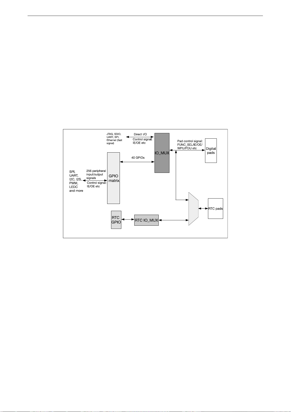
4.1 Introduction
The ESP32 chip features 40 physical GPIO pads. Some GPIO pads cannot be used or do not have the
corresponding pin on the chip package. Each pad can be used as a general purpose I/O or can be connected to
an internal peripheral signal. The IO_MUX, RTC IO_MUX and the GPIO matrix are responsible for routing signals
from the peripherals to GPIO pads. Together these systems provide highly configurable I/O.
This chapter describes the signal selection and connection between the digital pads (FUNC_SEL, IE, OE, WPU,
WDU, etc), 256 peripheral input/output signals (control signals: SIG_IN_SEL, SIG_OUT_SEL, IE, OE, etc), fast
peripheral input/output signals (control signals: SIG_IN_SEL, SIG_OUT_SEL, IE, OE, etc), and RTC
IO_MUX.
Figure 6: IO_MUX, RTC IO_MUX and GPIO Matrix Overview
1. The IO_MUX contains one register per GPIO pad. Each pad can be configured for ”GPIO” function
(connected to the GPIO Matrix) or configured for a direct function (bypassing the GPIO Matrix. Some high
speed digital functions (Ethernet, SDIO, SPI, JTAG, UART) can bypass the GPIO Matrix for better high
frequency digital performance. In this case, the IO_MUX is used to connect these pads directly to the
peripheral.)
Refer to Section 4.10 for a list of IO_MUX functions for each I/O pad.
2. The GPIO Matrix is a full switching matrix between the peripheral input/output signals and the pads.
• For input to the chip: Each of the 256 internal peripheral inputs can select any GPIO pad as the input
source.
• For output from the chip: The output signal of each of the 40 GPIO pads can be from one of the 256
peripheral output signals.
Refer to Section 4.9 for a list of GPIO Matrix peripheral signals.
3. RTC IO_MUX is used to connect GPIO pads to their low power and analog functions. Only a subset of
GPIO pads have these optional ”RTC” functions.
Espressif Systems 28 ESP32 Technical Reference Manual V1.0
Page 30
4.2 Peripheral Input via GPIO Matrix 4 IO_MUX AND GPIO MATRIX
GPIO_FUNCy_IN_SEL
GPIO0_in
GPIO1_in
GPIO2_in
GPIO3_in
GPIO39_in
0 (FUNC)
1 (FUNC)
2 (GPIO)
3
39
Peripheral Signal Y
I/O Pad X
In GPIO matrix
In IO MUX
GPIO X in
GPIOx_MCU_SEL
2
1
3
X
GPIOX_in
0
Constant 0 input
Constant 1 input
(0x30) 48
(0x38) 56
0
1 (GPIO)
GPIO_SIGxx_IN_SEL
GPIOx_FUN_IE = 1
Refer to Section 4.11 for a list of RTC IO_MUX functions.
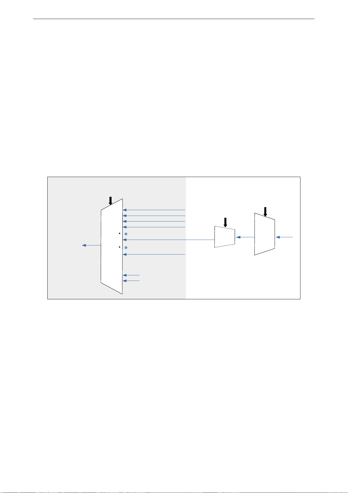
4.2 Peripheral Input via GPIO Matrix
4.2.1 Summary
To receive a peripheral input signal via the GPIO Matrix, the GPIO Matrix is configured to source the peripheral
signal’s input index (0-255) from one of the 40 GPIOs (0-39).
The input signal is read from the GPIO pad through the IO_MUX. The IO_MUX must be configured to set the
chosen pad to ”GPIO” function. This causes the GPIO pad input signal to be routed into the GPIO Matrix which
in turn routes it to the selected peripheral input.
4.2.2 Functional Description
Figure 7 shows the logic for input selection via GPIO Matrix.
To read GPIO pad X into peripheral signal Y, follow these steps:
Espressif Systems 29 ESP32 Technical Reference Manual V1.0
Figure 7: Peripheral Input via IO_MUX, GPIO Matrix
1. Configure the GPIO_FUNCy_IN_SEL_CFG register for peripheral signal Y in the GPIO Matrix:
• Set the GPIO_FUNCx_IN_SEL field to the number of the GPIO pad X to read from.
2. Configure the GPIO_FUNCx_OUT_SEL_CFG and GPIO_ENABLE_DATA[x] for GPIO pad X in the GPIO
Matrix:
• For input ony signals, the pad output can be disabled by setting the GPIO_FUNCx_OEN_SEL bits to
one and GPIO_ENABLE_DATA[x] to zero. Otherwise, there is no need to disable output.
3. Configure the IO_MUX register for GPIO pad X:
• Set the function field to GPIO.
• Enable the input by setting the xx_FUN_IE bit.
• Set xx_FUN_WPU and xx_FUN_WPD fields as desired to enable internal pull-up/pull-down resistors.
Page 31

4.3 Peripheral Output via GPIO Matrix 4 IO_MUX AND GPIO MATRIX
Notes:
• One input pad can be connected to multiple input_signals.
• The input signal can be inverted with GPIO_FUNCx_IN_INV_SEL.
• It is possible to have a peripheral read a constant low or constant high input value without connecting this
input to a pad. This can be done by selecting a special GPIO_FUNCy_IN_SEL input instead of a GPIO
number:
– When GPIO_FUNCx_IN_SEL is 0x30, input_signal_x is always 0
– When GPIO_FUNCx_IN_SEL is 0x38, input_signal_x is always 1.
4.2.3 Simple GPIO Input
The GPIO_IN_DATA register holds the input values of each GPIO pad.
The input value of any GPIO pin can be read at any time without configuring the GPIO Matrix for a particular
peripheral signal. However, it is necessary to configure the xx_FUN_IE register for pad X, as shown in Section
4.2.2.
4.3 Peripheral Output via GPIO Matrix
4.3.1 Summary
To output a signal from a peripheral via the GPIO Matrix, the GPIO Matrix is configured to route the peripheral
output signal (0-255) to one of the first 34 GPIOs (0-33). (Note that GPIO pads 34-39 cannot be used as
outputs.)
The output signal is routed from the peripheral into the GPIO Matrix. It is then routed into the IO_MUX, which is
configured to set the chosen pad to ”GPIO” function. This causes the output GPIO signal to be connected to the
pad.
4.3.2 Functional Description
One of 256 input signals can be selected to go through the GPIO matrix into the IO_MUX and then to a pad.
Figure 8 illustrates the configuration.
To output peripheral signal Y to particular GPIO pad X, follow these steps:
1. Configure the GPIO_FUNCx_OUT_SEL_CFG register and GPIO_ENABLE_DATA[x] of GPIO X in the GPIO
Matrix:
• Set GPIO_FUNCx_OUT_SEL to the index of desired peripheral output signal Y.
• Set the GPIO_FUNCx_OEN_SEL bits and GPIO_ENABLE_DATA[x] to enable output mode by force,
OR, clear GPIO_FUNCx_OEN_SEL to zero so that the output enable signal will be decided by the
internal logic function.
2. Optionally, to enable open drain mode set the GPIO_PINx_PAD_DRIVER bit in the GPIO_PINx register.
3. Configure the I/O mux register for GPIO pad X:
• Set the function field to GPIO.
Espressif Systems 30 ESP32 Technical Reference Manual V1.0
Page 32

4.4 Direct I/O via IO_MUX 4 IO_MUX AND GPIO MATRIX
GPIO_FUNCx_OUT_SEL
signal0_out
signal1_out
signal2_out
signal3_out
signal255_out
GPIO_OUT_DATA bit x
0
1
2
3
255
256
(0x100)
GPIOx_out
In GPIO matrix
In IO MUX
0 (FUNC)
1 (FUNC)
2 (GPIO)
I/O Pad X
GPIO X out
GPIOx_MCU_SEL
GPIOx_FUN_OE = 1
• Set the xx_FUN_DRV field to the desired value for output strength. The higher the value is, the higher
the output strength is. Pull up/down the pad by configuring xx_FUNC_WPU and xx_FUNC_WPD
registers in open drain mode.
Notes:
• The output signal from a single peripheral can be sent to multiple pads simultaneously.
• Only the first 34 GPIOs (0-33) can be used as outputs.
• The output signal can be inverted by setting the GPIO_FUNCx_OUT_INV_SEL bit.
Figure 8: Output via GPIO Matrix
4.3.3 Simple GPIO Output
The GPIO Matrix can also be used for simple GPIO output - setting a bit in the GPIO_OUT_DATA register will
write to the corresponding GPIO pad.
To configure a pad as simple GPIO output, the GPIO Matrix GPIO_FUNCx_OUT_SEL register is configured with a
special peripheral index value (0x100).
4.4 Direct I/O via IO_MUX
4.4.1 Summary
Some high speed digital functions (Ethernet, SDIO, SPI, JTAG, UART) can bypass the GPIO Matrix for better high
frequency digital performance. In this case, the IO_MUX is used to connect these pads directly to the
peripheral.
Selecting this option is less flexible than using the GPIO Matrix, as the IO_MUX register for each GPIO pad can
only select from a limited number of functions. However, better high frequency digital performance will be
maintained.
Espressif Systems 31 ESP32 Technical Reference Manual V1.0
Page 33

4.6 Light-sleep Mode Pin Functions 4 IO_MUX AND GPIO MATRIX
4.4.2 Functional Description
Two registers must be configured in order to bypass the GPIO Matrix for peripheral I/O:
1. IO_MUX for the GPIO pad must be set to the desired pad function (Section 4.10 has a list of pad functions).
2. For inputs, the SIG_IN_SEL register must be set to route the input directly to the peripheral.
4.5 RTC IO_MUX for Low Power and Analog I/O
4.5.1 Summary
18 pins have low power (RTC domain) capabilities and analog functions which are handled by the RTC
subsystem of ESP32. The IO_MUX and GPIO Matrix are not used for these functions, instead the RTC_MUX is
used to redirect the I/O to the RTC subsystem.
When configured as RTC GPIOs, the output pads can still retain the output level value when the chip is in
Deep-sleep mode, and the input pads can wake up the chip from Deep-sleep.
Section 4.11 has a list of RTC_MUX pins and their functions.
4.5.2 Functional Description
Each pad with analog and RTC functions is controlled by the RTC_IO_TOUCH_PADx_TO_GPIO bit in the
RTC_GPIO_PINx register. By default this bit is set to 1, routing all I/O via the IO_MUX subsystem as described in
earlier subsections.
If the RTC_IO_TOUCH_PADx_TO_GPIO bit is cleared, then I/O to and from that pad is routed to the RTC
subsystem instead. In this mode, the RTC_GPIO_PINx register is used for digital I/O and the analog features of
the pad are also available. See Section 4.11 for a list of RTC pin functions.
See 4.11 for a table mapping GPIO pads to their RTC equivalent pins and analog functions. Note that the
RTC_IO_PINx registers use the RTC GPIO pin numbering, not the GPIO pad numbering.
4.6 Light-sleep Mode Pin Functions
Pins can have different functions when the ESP32 is in Light-sleep mode. If the GPIOxx_SLP_SEL bit in the
IO_MUX register for a GPIO pad is set to 1, a different set of registers is used to control the pad when the ESP32
is in Light-sleep mode:
Table 15: IO_MUX Light-sleep Pin Function Registers
IO_MUX Function
Output Drive Strength GPIOxx_FUNC_DRV GPIOxx_MCU_DRV
Pullup Resistor GPIOxx_FUNC_WPU GPIOxx_MCU_WPU
Pulldown Resistor GPIOxx_FUNC_WPD GPIOxx_MCU_WPD
Output Enable (From GPIO Matrix _OEN field) GPIOxx_MCU_OE
If GPIOxx_SLP_SEL is set to 0, the pin functions remain the same in both normal execution and Light-sleep
modes.
Espressif Systems 32 ESP32 Technical Reference Manual V1.0
Normal Execution Light-sleep Mode
OR GPIOxx_SLP_SEL = 0 AND GPIOxx_SLP_SEL = 1
Page 34

4.7 Pad Hold Feature 4 IO_MUX AND GPIO MATRIX
4.7 Pad Hold Feature
Each IO pad (including the RTC pads) has an individual hold function controlled by a RTC register. When the pad
is set to hold, the state is latched at that moment and will not change no matter how the internal signals change
or how the IO_MUX configuration or GPIO configuration is modified. Users can use the hold function for the pads
to retain the pad state through a core reset and system reset triggered by watchdog time-out or Deep-sleep
events.
4.8 I/O Pad Power Supply
IO pad power supply is shown in Figure 9.
Figure 9: ESP32 I/O Pad Power Sources
• Pads marked blue are RTC pads that have their individual analog function and can also act as normal
digital IO pads. For details, please refer to Section 4.11.
• Pads marked pink and green only have digital functions.
• Pads marked green can be powered externally or internally via VDD_SDIO (see below).
4.8.1 VDD_SDIO Power Domain
VDD_SDIO can source or sink current, allowing this power domain to be powered externally or internally. To
power VDD_SDIO externally, apply the same power supply of VDD3P3_RTC to the VDD_SDIO pad.
Without an external power supply, the internal regulator will supply VDD_SDIO. The VDD_SDIO voltage can be
configured to be either 1.8V or 3.3V (the same as that at VRTC), depending on the state of the MTDI pad at reset
- a high level configures 1.8V and a low level configures 3.3V. Setting the efuse bit decides the default voltage of
the VDD_SDIO. In addition, software can change the voltage of the VDD_SDIO by configuring register bits.
Espressif Systems 33 ESP32 Technical Reference Manual V1.0
Page 35

4.9 Peripheral Signal List 4 IO_MUX AND GPIO MATRIX
4.9 Peripheral Signal List
Table 16 contains a list of Peripheral Input/Output signals used by the GPIO Matrix:
Table 16: GPIO Matrix Peripheral Signals
Signal Input Signal Output Signal Direct I/O in IO_MUX
0 SPICLK_in SPICLK_out YES
1 SPIQ_in SPIQ_out YES
2 SPID_in SPID_out YES
3 SPIHD_in SPIHD_out YES
4 SPIWP_in SPIWP_out YES
5 SPICS0_in SPICS0_out YES
6 SPICS1_in SPICS1_out
7 SPICS2_in SPICS2_out
8 HSPICLK_in HSPICLK_out YES
9 HSPIQ_in HSPIQ_out YES
10 HSPID_in HSPID_out YES
11 HSPICS0_in HSPICS0_out YES
12 HSPIHD_in HSPIHD_out YES
13 HSPIWP_in HSPIWP_out YES
14 U0RXD_in U0TXD_out YES
15 U0CTS_in U0RTS_out YES
16 U0DSR_in U0DTR_out
17 U1RXD_in U1TXD_out YES
18 U1CTS_in U1RTS_out YES
23 I2S0O_BCK_in I2S0O_BCK_out
24 I2S1O_BCK_in I2S1O_BCK_out
25 I2S0O_WS_in I2S0O_WS_out
26 I2S1O_WS_in I2S1O_WS_out
27 I2S0I_BCK_in I2S0I_BCK_out
28 I2S0I_WS_in I2S0I_WS_out
29 I2CEXT0_SCL_in I2CEXT0_SCL_out
30 I2CEXT0_SDA_in I2CEXT0_SDA_out
31 pwm0_sync0_in sdio_tohost_int_out
32 pwm0_sync1_in pwm0_out0a
33 pwm0_sync2_in pwm0_out0b
34 pwm0_f0_in pwm0_out1a
35 pwm0_f1_in pwm0_out1b
36 pwm0_f2_in pwm0_out2a
37 pwm0_out2b
39 pcnt_sig_ch0_in0
40 pcnt_sig_ch1_in0
41 pcnt_ctrl_ch0_in0
42 pcnt_ctrl_ch1_in0
43 pcnt_sig_ch0_in1
44 pcnt_sig_ch1_in1
Espressif Systems 34 ESP32 Technical Reference Manual V1.0
Page 36

4.9 Peripheral Signal List 4 IO_MUX AND GPIO MATRIX
Signal Input Signal Output Signal Direct I/O in IO_MUX
45 pcnt_ctrl_ch0_in1
46 pcnt_ctrl_ch1_in1
47 pcnt_sig_ch0_in2
48 pcnt_sig_ch1_in2
49 pcnt_ctrl_ch0_in2
50 pcnt_ctrl_ch1_in2
51 pcnt_sig_ch0_in3
52 pcnt_sig_ch1_in3
53 pcnt_ctrl_ch0_in3
54 pcnt_ctrl_ch1_in3
55 pcnt_sig_ch0_in4
56 pcnt_sig_ch1_in4
57 pcnt_ctrl_ch0_in4
58 pcnt_ctrl_ch1_in4
61 HSPICS1_in HSPICS1_out
62 HSPICS2_in HSPICS2_out
63 VSPICLK_in VSPICLK_out_mux YES
64 VSPIQ_in VSPIQ_out YES
65 VSPID_in VSPID_out YES
66 VSPIHD_in VSPIHD_out YES
67 VSPIWP_in VSPIWP_out YES
68 VSPICS0_in VSPICS0_out YES
69 VSPICS1_in VSPICS1_out
70 VSPICS2_in VSPICS2_out
71 pcnt_sig_ch0_in5 ledc_hs_sig_out0
72 pcnt_sig_ch1_in5 ledc_hs_sig_out1
73 pcnt_ctrl_ch0_in5 ledc_hs_sig_out2
74 pcnt_ctrl_ch1_in5 ledc_hs_sig_out3
75 pcnt_sig_ch0_in6 ledc_hs_sig_out4
76 pcnt_sig_ch1_in6 ledc_hs_sig_out5
77 pcnt_ctrl_ch0_in6 ledc_hs_sig_out6
78 pcnt_ctrl_ch1_in6 ledc_hs_sig_out7
79 pcnt_sig_ch0_in7 ledc_ls_sig_out0
80 pcnt_sig_ch1_in7 ledc_ls_sig_out1
81 pcnt_ctrl_ch0_in7 ledc_ls_sig_out2
82 pcnt_ctrl_ch1_in7 ledc_ls_sig_out3
83 rmt_sig_in0 ledc_ls_sig_out4
84 rmt_sig_in1 ledc_ls_sig_out5
85 rmt_sig_in2 ledc_ls_sig_out6
86 rmt_sig_in3 ledc_ls_sig_out7
87 rmt_sig_in4 rmt_sig_out0
88 rmt_sig_in5 rmt_sig_out1
89 rmt_sig_in6 rmt_sig_out2
90 rmt_sig_in7 rmt_sig_out3
Espressif Systems 35 ESP32 Technical Reference Manual V1.0
Page 37

4.9 Peripheral Signal List 4 IO_MUX AND GPIO MATRIX
Signal Input Signal Output Signal Direct I/O in IO_MUX
91 rmt_sig_out4
92 rmt_sig_out5
93 rmt_sig_out6
94 rmt_sig_out7
95 I2CEXT1_SCL_in I2CEXT1_SCL_out
96 I2CEXT1_SDA_in I2CEXT1_SDA_out
97 host_card_detect_n_1 host_ccmd_od_pullup_en_n
98 host_card_detect_n_2 host_rst_n_1
99 host_card_write_prt_1 host_rst_n_2
100 host_card_write_prt_2 gpio_sd0_out
101 host_card_int_n_1 gpio_sd1_out
102 host_card_int_n_2 gpio_sd2_out
103 pwm1_sync0_in gpio_sd3_out
104 pwm1_sync1_in gpio_sd4_out
105 pwm1_sync2_in gpio_sd5_out
106 pwm1_f0_in gpio_sd6_out
107 pwm1_f1_in gpio_sd7_out
108 pwm1_f2_in pwm1_out0a
109 pwm0_cap0_in pwm1_out0b
110 pwm0_cap1_in pwm1_out1a
111 pwm0_cap2_in pwm1_out1b
112 pwm1_cap0_in pwm1_out2a
113 pwm1_cap1_in pwm1_out2b
114 pwm1_cap2_in pwm2_out1h
115 pwm2_flta pwm2_out1l
116 pwm2_fltb pwm2_out2h
117 pwm2_cap1_in pwm2_out2l
118 pwm2_cap2_in pwm2_out3h
119 pwm2_cap3_in pwm2_out3l
120 pwm3_flta pwm2_out4h
121 pwm3_fltb pwm2_out4l
122 pwm3_cap1_in
123 pwm3_cap2_in
124 pwm3_cap3_in
140 I2S0I_DATA_in0 I2S0O_DATA_out0
141 I2S0I_DATA_in1 I2S0O_DATA_out1
142 I2S0I_DATA_in2 I2S0O_DATA_out2
143 I2S0I_DATA_in3 I2S0O_DATA_out3
144 I2S0I_DATA_in4 I2S0O_DATA_out4
145 I2S0I_DATA_in5 I2S0O_DATA_out5
146 I2S0I_DATA_in6 I2S0O_DATA_out6
147 I2S0I_DATA_in7 I2S0O_DATA_out7
148 I2S0I_DATA_in8 I2S0O_DATA_out8
149 I2S0I_DATA_in9 I2S0O_DATA_out9
Espressif Systems 36 ESP32 Technical Reference Manual V1.0
Page 38

4.9 Peripheral Signal List 4 IO_MUX AND GPIO MATRIX
Signal Input Signal Output Signal Direct I/O in IO_MUX
150 I2S0I_DATA_in10 I2S0O_DATA_out10
151 I2S0I_DATA_in11 I2S0O_DATA_out11
152 I2S0I_DATA_in12 I2S0O_DATA_out12
153 I2S0I_DATA_in13 I2S0O_DATA_out13
154 I2S0I_DATA_in14 I2S0O_DATA_out14
155 I2S0I_DATA_in15 I2S0O_DATA_out15
156 I2S0O_DATA_out16
157 I2S0O_DATA_out17
158 I2S0O_DATA_out18
159 I2S0O_DATA_out19
160 I2S0O_DATA_out20
161 I2S0O_DATA_out21
162 I2S0O_DATA_out22
163 I2S0O_DATA_out23
164 I2S1I_BCK_in I2S1I_BCK_out
165 I2S1I_WS_in I2S1I_WS_out
166 I2S1I_DATA_in0 I2S1O_DATA_out0
167 I2S1I_DATA_in1 I2S1O_DATA_out1
168 I2S1I_DATA_in2 I2S1O_DATA_out2
169 I2S1I_DATA_in3 I2S1O_DATA_out3
170 I2S1I_DATA_in4 I2S1O_DATA_out4
171 I2S1I_DATA_in5 I2S1O_DATA_out5
172 I2S1I_DATA_in6 I2S1O_DATA_out6
173 I2S1I_DATA_in7 I2S1O_DATA_out7
174 I2S1I_DATA_in8 I2S1O_DATA_out8
175 I2S1I_DATA_in9 I2S1O_DATA_out9
176 I2S1I_DATA_in10 I2S1O_DATA_out10
177 I2S1I_DATA_in11 I2S1O_DATA_out11
178 I2S1I_DATA_in12 I2S1O_DATA_out12
179 I2S1I_DATA_in13 I2S1O_DATA_out13
180 I2S1I_DATA_in14 I2S1O_DATA_out14
181 I2S1I_DATA_in15 I2S1O_DATA_out15
182 I2S1O_DATA_out16
183 I2S1O_DATA_out17
184 I2S1O_DATA_out18
185 I2S1O_DATA_out19
186 I2S1O_DATA_out20
187 I2S1O_DATA_out21
188 I2S1O_DATA_out22
189 I2S1O_DATA_out23
190 I2S0I_H_SYNC pwm3_out1h
191 I2S0I_V_SYNC pwm3_out1l
192 I2S0I_H_ENABLE pwm3_out2h
193 I2S1I_H_SYNC pwm3_out2l
Espressif Systems 37 ESP32 Technical Reference Manual V1.0
Page 39

4.10 IO_MUX Pad List 4 IO_MUX AND GPIO MATRIX
Signal Input Signal Output Signal Direct I/O in IO_MUX
194 I2S1I_V_SYNC pwm3_out3h
195 I2S1I_H_ENABLE pwm3_out3l
196 pwm3_out4h
197 pwm3_out4l
198 U2RXD_in U2TXD_out YES
199 U2CTS_in U2RTS_out YES
200 emac_mdc_i emac_mdc_o
201 emac_mdi_i emac_mdo_o
202 emac_crs_i emac_crs_o
203 emac_col_i emac_col_o
204 pcmfsync_in bt_audio0_irq
205 pcmclk_in bt_audio1_irq
206 pcmdin bt_audio2_irq
207 ble_audio0_irq
208 ble_audio1_irq
209 ble_audio2_irq
210 pcmfsync_out
211 pcmclk_out
212 pcmdout
213 ble_audio_sync0_p
214 ble_audio_sync1_p
215 ble_audio_sync2_p
224 sig_in_func224
225 sig_in_func225
226 sig_in_func226
227 sig_in_func227
228 sig_in_func228
Direct I/O in IO_MUX ”YES” means this signal is also available directly via IO_MUX. To apply GPIO Matrix for
these signals, their corresponding SIG_IN_SEL register must be cleared.
4.10 IO_MUX Pad List
Table 17 shows the IO_MUX functions for each I/O pad:
Table 17: IO_MUX Pad Summary
GPIO Pad Name Function 1 Function 2 Function 3 Function 4 Function 5 Function 6 Reset Notes
0 GPIO0 GPIO0 CLK_OUT1 GPIO0 - - EMAC_TX_CLK 3 R
1 U0TXD U0TXD CLK_OUT3 GPIO1 - - EMAC_RXD2 3 -
2 GPIO2 GPIO2 HSPIWP GPIO2 HS2_DATA0 SD_DATA0 - 2 R
3 U0RXD U0RXD CLK_OUT2 GPIO3 - - - 3 -
4 GPIO4 GPIO4 HSPIHD GPIO4 HS2_DATA1 SD_DATA1 EMAC_TX_ER 2 R
5 GPIO5 GPIO5 VSPICS0 GPIO5 HS1_DATA6 - EMAC_RX_CLK 3 -
6 SD_CLK SD_CLK SPICLK GPIO6 HS1_CLK U1CTS - 3 -
7 SD_DATA_0 SD_DATA0 SPIQ GPIO7 HS1_DATA0 U2RTS - 3 -
8 SD_DATA_1 SD_DATA1 SPID GPIO8 HS1_DATA1 U2CTS - 3 -
Espressif Systems 38 ESP32 Technical Reference Manual V1.0
Page 40

4.11 RTC_MUX Pin List 4 IO_MUX AND GPIO MATRIX
GPIO Pad Name Function 1 Function 2 Function 3 Function 4 Function 5 Function 6 Reset Notes
9 SD_DATA_2 SD_DATA2 SPIHD GPIO9 HS1_DATA2 U1RXD - 3 -
10 SD_DATA_3 SD_DATA3 SPIWP GPIO10 HS1_DATA3 U1TXD - 3 -
11 SD_CMD SD_CMD SPICS0 GPIO11 HS1_CMD U1RTS - 3 -
12 MTDI MTDI HSPIQ GPIO12 HS2_DATA2 SD_DATA2 EMAC_TXD3 2 R
13 MTCK MTCK HSPID GPIO13 HS2_DATA3 SD_DATA3 EMAC_RX_ER 1 R
14 MTMS MTMS HSPICLK GPIO14 HS2_CLK SD_CLK EMAC_TXD2 1 R
15 MTDO MTDO HSPICS0 GPIO15 HS2_CMD SD_CMD EMAC_RXD3 3 R
16 GPIO16 GPIO16 - GPIO16 HS1_DATA4 U2RXD EMAC_CLK_OUT 1 -
17 GPIO17 GPIO17 - GPIO17 HS1_DATA5 U2TXD EMAC_CLK_180 1 -
18 GPIO18 GPIO18 VSPICLK GPIO18 HS1_DATA7 - - 1 -
19 GPIO19 GPIO19 VSPIQ GPIO19 U0CTS - EMAC_TXD0 1 -
20 GPIO20 GPIO20 - GPIO20 - - - 1 -
21 GPIO21 GPIO21 VSPIHD GPIO21 - - EMAC_TX_EN 1 -
22 GPIO22 GPIO22 VSPIWP GPIO22 U0RTS - EMAC_TXD1 1 -
23 GPIO23 GPIO23 VSPID GPIO23 HS1_STROBE - - 1 -
25 GPIO25 GPIO25 - GPIO25 - - EMAC_RXD0 0 R
26 GPIO26 GPIO26 - GPIO26 - - EMAC_RXD1 0 R
27 GPIO27 GPIO27 - GPIO27 - - EMAC_RX_DV 1 R
32 32K_XP GPIO32 - GPIO32 - - - 0 R
33 32K_XN GPIO33 - GPIO33 - - - 0 R
34 VDET_1 GPIO34 - GPIO34 - - - 0 R, I
35 VDET_2 GPIO35 - GPIO35 - - - 0 R, I
36 SENSOR_VP GPIO36 - GPIO36 - - - 0 R, I
37 SENSOR_CAPP GPIO37 - GPIO37 - - - 0 R, I
38 SENSOR_CAPN GPIO38 - GPIO38 - - - 0 R, I
39 SENSOR_VN GPIO39 - GPIO39 - - - 0 R, I
Reset Configurations
”Reset” column shows each pad’s default configurations after reset:
• 0 - IE=0 (input disabled).
• 1 - IE=1 (input enabled).
• 2 - IE=1, WPD=1 (input enabled, pulldown resistor).
• 3 - IE=1, WPU=1 (input enabled, pullup resistor).
Notes
• R - Pad has RTC/analog functions via RTC_MUX.
• I - Pad can only be configured as input GPIO.
Refer to ESP32 Pin List datasheet for more details and a complete table of pin functions.
4.11 RTC_MUX Pin List
Table 18 shows the RTC pins and how they correspond to GPIO pads:
Table 18: RTC_MUX Pin Summary
RTC GPIO Num GPIO Num Pad Name
1 2 3
Analog Function
0 36 SENSOR_VP ADC_H ADC1_CH0 -
1 37 SENSOR_CAPP ADC_H ADC1_CH1 -
Espressif Systems 39 ESP32 Technical Reference Manual V1.0
Page 41

4.12 Register Summary 4 IO_MUX AND GPIO MATRIX
RTC GPIO Num GPIO Num Pad Name
2 38 SENSOR_CAPN ADC_H ADC1_CH2 -
3 39 SENSOR_VN ADC_H ADC1_CH3 -
4 34 VDET_1 - ADC1_CH6 -
5 35 VDET_2 - ADC1_CH7 -
6 25 GPIO25 DAC_1 ADC2_CH8 -
7 26 GPIO26 DAC_2 ADC2_CH9 -
8 33 32K_XN XTAL_32K_N ADC1_CH5 TOUCH8
9 32 32K_XP XTAL_32K_P ADC1_CH4 TOUCH9
10 4 GPIO4 - ADC2_CH0 TOUCH0
11 0 GPIO0 - ADC2_CH1 TOUCH1
12 2 GPIO2 - ADC2_CH2 TOUCH2
13 15 MTDO - ADC2_CH3 TOUCH3
14 13 MTCK - ADC2_CH4 TOUCH4
15 12 MTDI - ADC2_CH5 TOUCH5
16 14 MTMS - ADC2_CH6 TOUCH6
17 27 GPIO27 - ADC2_CH7 TOUCH7
1 2 3
Analog Function
4.12 Register Summary
Name Description Address Access
GPIO_OUT_REG GPIO 0-31 output register_REG 0x3FF44004 R/W
GPIO_OUT_W1TS_REG GPIO 0-31 output register_W1TS_REG 0x3FF44008 RO
GPIO_OUT_W1TC_REG GPIO 0-31 output register_W1TC_REG 0x3FF4400C RO
GPIO_OUT1_REG GPIO 0-31 output register1_REG 0x3FF44010 R/W
GPIO_OUT1_W1TS_REG GPIO 0-31 output register1_W1TS_REG 0x3FF44014 RO
GPIO_OUT1_W1TC_REG GPIO 0-31 output register1_W1TC_REG 0x3FF44018 RO
GPIO_OUT_W1TS_REG GPIO 0-31 output bit set register_REG 0x3FF44008 RO
GPIO_OUT_W1TC_REG GPIO 0-31 output bit clear register_REG 0x3FF4400C RO
GPIO_OUT1_REG GPIO 32-39 output register_REG 0x3FF44010 R/W
GPIO_OUT1_W1TS_REG GPIO 32-39 output register_W1TS_REG 0x3FF44014 RO
GPIO_OUT1_W1TC_REG GPIO 32-39 output register_W1TC_REG 0x3FF44018 RO
GPIO_OUT1_W1TS_REG GPIO 32-39 output bit set register_REG 0x3FF44014 RO
GPIO_OUT1_W1TC_REG GPIO 32-39 output bit clear register_REG 0x3FF44018 RO
GPIO_ENABLE_REG GPIO 0-31 output enable register_REG 0x3FF44020 R/W
GPIO_ENABLE_W1TS_REG GPIO 0-31 output enable register_W1TS_REG 0x3FF44024 RO
GPIO_ENABLE_W1TC_REG GPIO 0-31 output enable register_W1TC_REG 0x3FF44028 RO
GPIO_ENABLE1_REG GPIO 0-31 output enable register1_REG 0x3FF4402C R/W
GPIO_ENABLE1_W1TS_REG GPIO 0-31 output enable register1_W1TS_REG 0x3FF44030 RO
GPIO_ENABLE1_W1TC_REG GPIO 0-31 output enable register1_W1TC_REG 0x3FF44034 RO
GPIO_ENABLE_W1TS_REG GPIO 0-31 output enable bit set register_REG 0x3FF44024 RO
GPIO_ENABLE_W1TC_REG GPIO 0-31 output enable bit clear register_REG 0x3FF44028 RO
GPIO_ENABLE1_REG GPIO 32-39 output enable register_REG 0x3FF4402C R/W
Espressif Systems 40 ESP32 Technical Reference Manual V1.0
Page 42

4.12 Register Summary 4 IO_MUX AND GPIO MATRIX
Name Description Address Access
GPIO_ENABLE1_W1TS_REG GPIO 32-39 output enable register_W1TS_REG 0x3FF44030 RO
GPIO_ENABLE1_W1TC_REG GPIO 32-39 output enable register_W1TC_REG 0x3FF44034 RO
GPIO_ENABLE1_W1TS_REG GPIO 32-39 output enable bit set register_REG 0x3FF44030 RO
GPIO_ENABLE1_W1TC_REG GPIO 32-39 output enable bit clear register_REG 0x3FF44034 RO
GPIO_STRAP_REG Bootstrap pin value register_REG 0x3FF44038 RO
GPIO_IN_REG GPIO 0-31 input register_REG 0x3FF4403C RO
GPIO_IN1_REG GPIO 0-31 input register1_REG 0x3FF44040 RO
GPIO_IN1_REG GPIO 32-39 input register_REG 0x3FF44040 RO
GPIO_STATUS_REG GPIO 0-31 interrupt status register_REG 0x3FF44044 R/W
GPIO_STATUS_W1TS_REG GPIO 0-31 interrupt status register_W1TS_REG 0x3FF44048 RO
GPIO_STATUS_W1TC_REG GPIO 0-31 interrupt status register_W1TC_REG 0x3FF4404C RO
GPIO_STATUS1_REG GPIO 0-31 interrupt status register1_REG 0x3FF44050 R/W
GPIO_STATUS1_W1TS_REG GPIO 0-31 interrupt status register1_W1TS_REG 0x3FF44054 RO
GPIO_STATUS1_W1TC_REG GPIO 0-31 interrupt status register1_W1TC_REG 0x3FF44058 RO
GPIO_STATUS_W1TS_REG GPIO 0-31 interrupt status bit set register_REG 0x3FF44048 RO
GPIO_STATUS_W1TC_REG GPIO 0-31 interrupt status bit clear register_REG 0x3FF4404C RO
GPIO_STATUS1_REG GPIO 32-39 interrupt status register_REG 0x3FF44050 R/W
GPIO_STATUS1_W1TS_REG GPIO 32-39 interrupt status register_W1TS_REG 0x3FF44054 RO
GPIO_STATUS1_W1TC_REG GPIO 32-39 interrupt status register_W1TC_REG 0x3FF44058 RO
GPIO_STATUS1_W1TS_REG GPIO 32-39 interrupt status bit set register_REG 0x3FF44054 RO
GPIO_STATUS1_W1TC_REG GPIO 32-39 interrupt status bit clear register_REG 0x3FF44058 RO
GPIO_ACPU_INT_REG GPIO 0-31 APP_CPU interrupt status_REG 0x3FF44060 RO
GPIO_ACPU_INT1_REG GPIO 0-31 APP_CPU interrupt status1_REG 0x3FF44074 RO
GPIO_ACPU_NMI_INT_REG
GPIO_ACPU_NMI_INT1_REG
GPIO 0-31 APP_CPU non-maskable interrupt sta-
tus_REG
GPIO 0-31 APP_CPU non-maskable interrupt sta-
tus1_REG
0x3FF44064 RO
0x3FF44078 RO
GPIO_PCPU_INT_REG GPIO 0-31 PRO_CPU interrupt status_REG 0x3FF44068 RO
GPIO_PCPU_INT1_REG GPIO 0-31 PRO_CPU interrupt status1_REG 0x3FF4407C RO
GPIO_PCPU_NMI_INT_REG
GPIO_PCPU_NMI_INT1_REG
GPIO 0-31 PRO_CPU non-maskable interrupt sta-
tus_REG
GPIO 0-31 PRO_CPU non-maskable interrupt sta-
tus1_REG
0x3FF4406C RO
0x3FF44080 RO
GPIO_ACPU_INT1_REG GPIO 32-39 APP_CPU interrupt status_REG 0x3FF44074 RO
GPIO_ACPU_NMI_INT1_REG
GPIO 32-39 APP_CPU non-maskable interrupt
status_REG
0x3FF44078 RO
GPIO_PCPU_INT1_REG GPIO 32-39 PRO_CPU interrupt status_REG 0x3FF4407C RO
GPIO_PCPU_NMI_INT1_REG
GPIO 32-39 PRO_CPU non-maskable interrupt
status_REG
0x3FF44080 RO
GPIO_PIN0_REG Configuration for GPIO pin 0_REG 0x3FF44088 R/W
GPIO_PIN1_REG Configuration for GPIO pin 1_REG 0x3FF4408C R/W
GPIO_PIN2_REG Configuration for GPIO pin 2_REG 0x3FF44090 R/W
... ...
GPIO_PIN38_REG Configuration for GPIO pin 38_REG 0x3FF44120 R/W
Espressif Systems 41 ESP32 Technical Reference Manual V1.0
Page 43

4.12 Register Summary 4 IO_MUX AND GPIO MATRIX
Name Description Address Access
GPIO_PIN39_REG Configuration for GPIO pin 39_REG 0x3FF44124 R/W
GPIO_FUNC0_IN_SEL_CFG_REG Peripheral function 0 input selection register_REG 0x3FF44130 R/W
GPIO_FUNC1_IN_SEL_CFG_REG Peripheral function 1 input selection register_REG 0x3FF44134 R/W
... ...
GPIO_FUNC254_IN_SEL_CFG_REG
GPIO_FUNC255_IN_SEL_CFG_REG
Peripheral function 254 input selection regis-
ter_REG
Peripheral function 255 input selection regis-
ter_REG
0x3FF44528 R/W
0x3FF4452C R/W
GPIO_FUNC0_OUT_SEL_CFG_REG Peripheral output selection for GPIO 0_REG 0x3FF44530 R/W
GPIO_FUNC1_OUT_SEL_CFG_REG Peripheral output selection for GPIO 1_REG 0x3FF44534 R/W
... ...
GPIO_FUNC38_OUT_SEL_CFG_REG Peripheral output selection for GPIO 38_REG 0x3FF445C8 R/W
GPIO_FUNC39_OUT_SEL_CFG_REG Peripheral output selection for GPIO 39_REG 0x3FF445CC R/W
Name Description Address Access
IO_MUX_GPIO36_REG Configuration register for pad GPIO36 0x3FF53004 R/W
IO_MUX_GPIO37_REG Configuration register for pad GPIO37 0x3FF53008 R/W
IO_MUX_GPIO38_REG Configuration register for pad GPIO38 0x3FF5300C R/W
IO_MUX_GPIO39_REG Configuration register for pad GPIO39 0x3FF53010 R/W
IO_MUX_GPIO34_REG Configuration register for pad GPIO34 0x3FF53014 R/W
IO_MUX_GPIO35_REG Configuration register for pad GPIO35 0x3FF53018 R/W
IO_MUX_GPIO32_REG Configuration register for pad GPIO32 0x3FF5301C R/W
IO_MUX_GPIO33_REG Configuration register for pad GPIO33 0x3FF53020 R/W
IO_MUX_GPIO25_REG Configuration register for pad GPIO25 0x3FF53024 R/W
IO_MUX_GPIO26_REG Configuration register for pad GPIO26 0x3FF53028 R/W
IO_MUX_GPIO27_REG Configuration register for pad GPIO27 0x3FF5302C R/W
IO_MUX_MTMS_REG Configuration register for pad MTMS 0x3FF53030 R/W
IO_MUX_MTDI_REG Configuration register for pad MTDI 0x3FF53034 R/W
IO_MUX_MTCK_REG Configuration register for pad MTCK 0x3FF53038 R/W
IO_MUX_MTDO_REG Configuration register for pad MTDO 0x3FF5303C R/W
IO_MUX_GPIO2_REG Configuration register for pad GPIO2 0x3FF53040 R/W
IO_MUX_GPIO0_REG Configuration register for pad GPIO0 0x3FF53044 R/W
IO_MUX_GPIO4_REG Configuration register for pad GPIO4 0x3FF53048 R/W
IO_MUX_GPIO16_REG Configuration register for pad GPIO16 0x3FF5304C R/W
IO_MUX_GPIO17_REG Configuration register for pad GPIO17 0x3FF53050 R/W
IO_MUX_SD_DATA2_REG Configuration register for pad SD_DATA2 0x3FF53054 R/W
IO_MUX_SD_DATA3_REG Configuration register for pad SD_DATA3 0x3FF53058 R/W
IO_MUX_SD_CMD_REG Configuration register for pad SD_CMD 0x3FF5305C R/W
IO_MUX_SD_CLK_REG Configuration register for pad SD_CLK 0x3FF53060 R/W
IO_MUX_SD_DATA0_REG Configuration register for pad SD_DATA0 0x3FF53064 R/W
IO_MUX_SD_DATA1_REG Configuration register for pad SD_DATA1 0x3FF53068 R/W
IO_MUX_GPIO5_REG Configuration register for pad GPIO5 0x3FF5306C R/W
IO_MUX_GPIO18_REG Configuration register for pad GPIO18 0x3FF53070 R/W
IO_MUX_GPIO19_REG Configuration register for pad GPIO19 0x3FF53074 R/W
Espressif Systems 42 ESP32 Technical Reference Manual V1.0
Page 44

4.12 Register Summary 4 IO_MUX AND GPIO MATRIX
Name Description Address Access
IO_MUX_GPIO20_REG Configuration register for pad GPIO20 0x3FF53078 R/W
IO_MUX_GPIO21_REG Configuration register for pad GPIO21 0x3FF5307C R/W
IO_MUX_GPIO22_REG Configuration register for pad GPIO22 0x3FF53080 R/W
IO_MUX_U0RXD_REG Configuration register for pad U0RXD 0x3FF53084 R/W
IO_MUX_U0TXD_REG Configuration register for pad U0TXD 0x3FF53088 R/W
IO_MUX_GPIO23_REG Configuration register for pad GPIO23 0x3FF5308C R/W
IO_MUX_GPIO24_REG Configuration register for pad GPIO24 0x3FF53090 R/W
Name Description Address Access
GPIO configuration / data registers
RTCIO_RTC_GPIO_OUT_REG RTC GPIO output register_REG 0x3FF48000 R/W
RTCIO_RTC_GPIO_OUT_W1TS_REG RTC GPIO output register_W1TS_REG 0x3FF48001 WO
RTCIO_RTC_GPIO_OUT_W1TC_REG RTC GPIO output register_W1TC_REG 0x3FF48002 WO
RTCIO_RTC_GPIO_OUT_W1TS_REG RTC GPIO output bit set register_REG 0x3FF48001 WO
RTCIO_RTC_GPIO_OUT_W1TC_REG RTC GPIO output bit clear register_REG 0x3FF48002 WO
RTCIO_RTC_GPIO_ENABLE_REG RTC GPIO output enable register_REG 0x3FF48003 R/W
RTCIO_RTC_GPIO_ENABLE_W1TS_REG RTC GPIO output enable register_W1TS_REG 0x3FF48004 WO
RTCIO_RTC_GPIO_ENABLE_W1TC_REG RTC GPIO output enable register_W1TC_REG 0x3FF48005 WO
RTCIO_RTC_GPIO_ENABLE_W1TS_REG RTC GPIO output enable bit setregister_REG 0x3FF48004 WO
RTCIO_RTC_GPIO_ENABLE_W1TC_REG RTC GPIO output enable bit clear register_REG 0x3FF48005 WO
RTCIO_RTC_GPIO_STATUS_REG RTC GPIO interrupt status register_REG 0x3FF48006 R/W
RTCIO_RTC_GPIO_STATUS_W1TS_REG
RTCIO_RTC_GPIO_STATUS_W1TC_REG
RTC GPIO interrupt status regis-
ter_W1TS_REG
RTC GPIO interrupt status regis-
ter_W1TC_REG
0x3FF48007 WO
0x3FF48008 WO
RTCIO_RTC_GPIO_STATUS_W1TS_REG RTC GPIO interrupt status bit set register_REG 0x3FF48007 WO
RTCIO_RTC_GPIO_STATUS_W1TC_REG
RTC GPIO interrupt status bit clear regis-
ter_REG
0x3FF48008 WO
RTCIO_RTC_GPIO_IN_REG RTC GPIO input register_REG 0x3FF48009 RO
RTCIO_RTC_GPIO_PIN0_REG RTC configuration for pin 0_REG 0x3FF4800A R/W
RTCIO_RTC_GPIO_PIN1_REG RTC configuration for pin 1_REG 0x3FF4800B R/W
RTCIO_RTC_GPIO_PIN2_REG RTC configuration for pin 2_REG 0x3FF4800C R/W
RTCIO_RTC_GPIO_PIN3_REG RTC configuration for pin 3_REG 0x3FF4800D R/W
RTCIO_RTC_GPIO_PIN4_REG RTC configuration for pin 4_REG 0x3FF4800E R/W
RTCIO_RTC_GPIO_PIN5_REG RTC configuration for pin 5_REG 0x3FF4800F R/W
RTCIO_RTC_GPIO_PIN6_REG RTC configuration for pin 6_REG 0x3FF48010 R/W
RTCIO_RTC_GPIO_PIN7_REG RTC configuration for pin 7_REG 0x3FF48011 R/W
RTCIO_RTC_GPIO_PIN8_REG RTC configuration for pin 8_REG 0x3FF48012 R/W
RTCIO_RTC_GPIO_PIN9_REG RTC configuration for pin 9_REG 0x3FF48013 R/W
RTCIO_RTC_GPIO_PIN10_REG RTC configuration for pin 10_REG 0x3FF48014 R/W
RTCIO_RTC_GPIO_PIN11_REG RTC configuration for pin 11_REG 0x3FF48015 R/W
RTCIO_RTC_GPIO_PIN12_REG RTC configuration for pin 12_REG 0x3FF48016 R/W
RTCIO_RTC_GPIO_PIN13_REG RTC configuration for pin 13_REG 0x3FF48017 R/W
RTCIO_RTC_GPIO_PIN14_REG RTC configuration for pin 14_REG 0x3FF48018 R/W
Espressif Systems 43 ESP32 Technical Reference Manual V1.0
Page 45

4.12 Register Summary 4 IO_MUX AND GPIO MATRIX
Name Description Address Access
RTCIO_RTC_GPIO_PIN15_REG RTC configuration for pin 15_REG 0x3FF48019 R/W
RTCIO_RTC_GPIO_PIN16_REG RTC configuration for pin 16_REG 0x3FF4801A R/W
RTCIO_RTC_GPIO_PIN17_REG RTC configuration for pin 17_REG 0x3FF4801B R/W
RTCIO_DIG_PAD_HOLD_REG RTC GPIO hold register_REG 0x3FF4801D R/W
GPIO RTC functions configuration registers
RTCIO_HALL_SENS_REG Hall sensor configuration_REG 0x3FF4801E R/W
RTCIO_SENSOR_PADS_REG Sensor pads configuration register_REG 0x3FF4801F R/W
RTCIO_ADC_PAD_REG ADC configuration register_REG 0x3FF48020 R/W
RTCIO_PAD_DAC1_REG DAC1 configuration register_REG 0x3FF48021 R/W
RTCIO_PAD_DAC2_REG DAC2 configuration register_REG 0x3FF48022 R/W
RTCIO_XTAL_32K_PAD_REG 32KHz crystal pads configuration register_REG 0x3FF48023 R/W
RTCIO_TOUCH_CFG_REG Touch sensor configuration register_REG 0x3FF48024 R/W
RTCIO_EXT_WAKEUP0_REG External wake up configuration register_REG 0x3FF4802F R/W
RTCIO_XTL_EXT_CTR_REG Crystal power down enable gpio source_REG 0x3FF48030 R/W
RTCIO_SAR_I2C_IO_REG RTC I2C pad selection_REG 0x3FF48031 R/W
Espressif Systems 44 ESP32 Technical Reference Manual V1.0
Page 46

4.13 Registers 4 IO_MUX AND GPIO MATRIX
4.13 Registers
Register 4.1: GPIO_OUT_REG (0x0004)
31 0
x x x x x x x x x x x x x x x x x x x x x x x x x x x x x x x x
GPIO_OUT_REG GPIO0-31 output value. (R/W)
Register 4.2: GPIO_OUT_W1TS_REG (0x0008)
31 0
x x x x x x x x x x x x x x x x x x x x x x x x x x x x x x x x
GPIO_OUT_W1TS_REG GPIO0-31 output set register. For every bit that is one in the value that is
written here, the corresponding bit in GPIO_OUT_DATA will be set. (RO)
Reset
Reset
Register 4.3: GPIO_OUT_W1TC_REG (0x000c)
31 0
x x x x x x x x x x x x x x x x x x x x x x x x x x x x x x x x
GPIO_OUT_W1TC_REG GPIO0-31 output clear register. For every bit that is one in the value that is
written here, the corresponding bit in GPIO_OUT_DATA will be cleared. (RO)
Register 4.4: GPIO_OUT1_REG (0x0010)
(reserved)
31 8
0 0 0 0 0 0 0 0 0 0 0 0 0 0 0 0 0 0 0 0 0 0 0 0
7 0
x x x x x x x x
GPIO_OUT_DATA
GPIO_OUT_DATA GPIO32-39 output value. (R/W)
Reset
Reset
Espressif Systems 45 ESP32 Technical Reference Manual V1.0
Page 47

4.13 Registers 4 IO_MUX AND GPIO MATRIX
Register 4.5: GPIO_OUT1_W1TS_REG (0x0014)
(reserved)
31 8
0 0 0 0 0 0 0 0 0 0 0 0 0 0 0 0 0 0 0 0 0 0 0 0
7 0
x x x x x x x x
GPIO_OUT_DATA
GPIO_OUT_DATA GPIO32-39 output value set register. For every bit that is one in the value that is
written here, the corresponding bit in GPIO_OUT1_DATA will be set. (RO)
Register 4.6: GPIO_OUT1_W1TC_REG (0x0018)
(reserved)
31 8
0 0 0 0 0 0 0 0 0 0 0 0 0 0 0 0 0 0 0 0 0 0 0 0
7 0
x x x x x x x x
GPIO_OUT_DATA
GPIO_OUT_DATA GPIO32-39 output value clear register. For every bit that is one in the value that is
written here, the corresponding bit in GPIO_OUT1_DATA will be cleared. (RO)
Reset
Reset
Register 4.7: GPIO_ENABLE_REG (0x0020)
31 0
x x x x x x x x x x x x x x x x x x x x x x x x x x x x x x x x
GPIO_ENABLE_REG GPIO0-31 output enable. (R/W)
Register 4.8: GPIO_ENABLE_W1TS_REG (0x0024)
31 0
x x x x x x x x x x x x x x x x x x x x x x x x x x x x x x x x
GPIO_ENABLE_W1TS_REG GPIO0-31 output enable set register. For every bit that is one in the
value that is written here, the corresponding bit in GPIO_ENABLE will be set. (RO)
Register 4.9: GPIO_ENABLE_W1TC_REG (0x0028)
31 0
x x x x x x x x x x x x x x x x x x x x x x x x x x x x x x x x
Reset
Reset
Reset
GPIO_ENABLE_W1TC_REG GPIO0-31 output enable clear register. For every bit that is one in the
value that is written here, the corresponding bit in GPIO_ENABLE will be cleared. (RO)
Espressif Systems 46 ESP32 Technical Reference Manual V1.0
Page 48

4.13 Registers 4 IO_MUX AND GPIO MATRIX
Register 4.10: GPIO_ENABLE1_REG (0x002c)
(reserved)
31 8
0 0 0 0 0 0 0 0 0 0 0 0 0 0 0 0 0 0 0 0 0 0 0 0
7 0
x x x x x x x x
GPIO_ENABLE_DATA
GPIO_ENABLE_DATA GPIO32-39 output enable. (R/W)
Register 4.11: GPIO_ENABLE1_W1TS_REG (0x0030)
(reserved)
31 8
0 0 0 0 0 0 0 0 0 0 0 0 0 0 0 0 0 0 0 0 0 0 0 0
7 0
x x x x x x x x
GPIO_ENABLE_DATA
GPIO_ENABLE_DATA GPIO32-39 output enable set register. For every bit that is one in the value
that is written here, the corresponding bit in GPIO_ENABLE1 will be set. (RO)
Reset
Reset
Register 4.12: GPIO_ENABLE1_W1TC_REG (0x0034)
(reserved)
31 8
0 0 0 0 0 0 0 0 0 0 0 0 0 0 0 0 0 0 0 0 0 0 0 0
7 0
x x x x x x x x
GPIO_ENABLE_DATA
GPIO_ENABLE_DATA GPIO32-39 output enable clear register. For every bit that is one in the value
that is written here, the corresponding bit in GPIO_ENABLE1 will be cleared. (RO)
Register 4.13: GPIO_STRAP_REG (0x0038)
(reserved)
31 16
0 0 0 0 0 0 0 0 0 0 0 0 0 0 0 0
15 0
x x x x x x x x x x x x x x x x
GPIO_STRAPPING
Reset
Reset
GPIO_STRAPPING GPIO strapping results: boot_sel_chip[5:0]: MTDI, GPIO0, GPIO2, GPIO4,
MTDO, GPIO5.
Espressif Systems 47 ESP32 Technical Reference Manual V1.0
Page 49

4.13 Registers 4 IO_MUX AND GPIO MATRIX
Register 4.14: GPIO_IN_REG (0x003c)
31 0
x x x x x x x x x x x x x x x x x x x x x x x x x x x x x x x x
Reset
GPIO_IN_REG GPIO0-31 input value. Each bit represents pad input value, 1 for high level and 0 for
low level. (RO)
Register 4.15: GPIO_IN1_REG (0x0040)
(reserved)
31 8
0 0 0 0 0 0 0 0 0 0 0 0 0 0 0 0 0 0 0 0 0 0 0 0
7 0
x x x x x x x x
GPIO_IN_DATA_NEXT
GPIO_IN_DATA_NEXT GPIO32-39 input value. Each bit represents pad input value. (RO)
Register 4.16: GPIO_STATUS_REG (0x0044)
31 0
x x x x x x x x x x x x x x x x x x x x x x x x x x x x x x x x
GPIO_STATUS_REG GPIO0-31 interrupt status register. Each bit can be the two interrupt sources
for the two CPUs. The enable bits in GPIO_STATUS_INTERRUPT corresponding to the 0-4 bits in
GPIO_PINn_REG should be set to 1. (R/W)
Register 4.17: GPIO_STATUS_W1TS_REG (0x0048)
31 0
x x x x x x x x x x x x x x x x x x x x x x x x x x x x x x x x
Reset
Reset
Reset
GPIO_STATUS_W1TS_REG GPIO0-31 interrupt status set register. For every bit that is one in the
value that is written here, the corresponding bit in GPIO_STATUS_INTERRUPT will be set. (RO)
Register 4.18: GPIO_STATUS_W1TC_REG (0x004c)
31 0
x x x x x x x x x x x x x x x x x x x x x x x x x x x x x x x x
Reset
GPIO_STATUS_W1TC_REG GPIO0-31 interrupt status clear register. For every bit that is one in the
value that is written here, the corresponding bit in GPIO_STATUS_INTERRUPT will be cleared. (RO)
Espressif Systems 48 ESP32 Technical Reference Manual V1.0
Page 50

4.13 Registers 4 IO_MUX AND GPIO MATRIX
Register 4.19: GPIO_STATUS1_REG (0x0050)
(reserved)
31 8
0 0 0 0 0 0 0 0 0 0 0 0 0 0 0 0 0 0 0 0 0 0 0 0
7 0
x x x x x x x x
GPIO_STATUS_INTERRUPT
GPIO_STATUS_INTERRUPT GPIO32-39 interrupt status. (R/W)
Register 4.20: GPIO_STATUS1_W1TS_REG (0x0054)
(reserved)
31 8
0 0 0 0 0 0 0 0 0 0 0 0 0 0 0 0 0 0 0 0 0 0 0 0
7 0
x x x x x x x x
GPIO_STATUS_INTERRUPT
GPIO_STATUS_INTERRUPT GPIO32-39 interrupt status set register. For every bit that is one in the
value that is written here, the corresponding bit in GPIO_STATUS_INTERRUPT1 will be set. (RO)
Reset
Reset
Register 4.21: GPIO_STATUS1_W1TC_REG (0x0058)
(reserved)
31 8
0 0 0 0 0 0 0 0 0 0 0 0 0 0 0 0 0 0 0 0 0 0 0 0
7 0
x x x x x x x x
GPIO_STATUS_INTERRUPT
GPIO_STATUS_INTERRUPT GPIO32-39 interrupt status clear register. For every bit that is one in
the value that is written here, the corresponding bit in GPIO_STATUS_INTERRUPT1 will be cleared.
(RO)
Register 4.22: GPIO_ACPU_INT_REG (0x0060)
31 0
x x x x x x x x x x x x x x x x x x x x x x x x x x x x x x x x
Reset
Reset
GPIO_ACPU_INT_REG GPIO0-31 APP CPU interrupt status. (RO)
Espressif Systems 49 ESP32 Technical Reference Manual V1.0
Page 51

4.13 Registers 4 IO_MUX AND GPIO MATRIX
Register 4.23: GPIO_ACPU_NMI_INT_REG (0x0064)
31 0
x x x x x x x x x x x x x x x x x x x x x x x x x x x x x x x x
Reset
GPIO_ACPU_NMI_INT_REG GPIO0-31 APP CPU non-maskable interrupt status. (RO)
Register 4.24: GPIO_PCPU_INT_REG (0x0068)
31 0
x x x x x x x x x x x x x x x x x x x x x x x x x x x x x x x x
Reset
GPIO_PCPU_INT_REG GPIO0-31 PRO CPU interrupt status. (RO)
Register 4.25: GPIO_PCPU_NMI_INT_REG (0x006c)
31 0
x x x x x x x x x x x x x x x x x x x x x x x x x x x x x x x x
GPIO_PCPU_NMI_INT_REG GPIO0-31 PRO CPU non-maskable interrupt status. (RO)
Register 4.26: GPIO_ACPU_INT1_REG (0x0074)
(reserved)
31 8
0 0 0 0 0 0 0 0 0 0 0 0 0 0 0 0 0 0 0 0 0 0 0 0
7 0
x x x x x x x x
GPIO_APPCPU_INT
GPIO_APPCPU_INT GPIO32-39 APP CPU interrupt status. (RO)
Register 4.27: GPIO_ACPU_NMI_INT1_REG (0x0078)
Reset
Reset
(reserved)
31 8
0 0 0 0 0 0 0 0 0 0 0 0 0 0 0 0 0 0 0 0 0 0 0 0
7 0
x x x x x x x x
GPIO_APPCPU_NMI_INT
Reset
GPIO_APPCPU_NMI_INT GPIO32-39 APP CPU non-maskable interrupt status. (RO)
Espressif Systems 50 ESP32 Technical Reference Manual V1.0
Page 52

4.13 Registers 4 IO_MUX AND GPIO MATRIX
Register 4.28: GPIO_PCPU_INT1_REG (0x007c)
(reserved)
31 8
0 0 0 0 0 0 0 0 0 0 0 0 0 0 0 0 0 0 0 0 0 0 0 0
7 0
x x x x x x x x
GPIO_PROCPU_INT GPIO32-39 PRO CPU interrupt status. (RO)
Register 4.29: GPIO_PCPU_NMI_INT1_REG (0x0080)
(reserved)
31 8
0 0 0 0 0 0 0 0 0 0 0 0 0 0 0 0 0 0 0 0 0 0 0 0
7 0
x x x x x x x x
GPIO_PROCPU_NMI_INT GPIO32-39 PRO CPU non-maskable interrupt status. (RO)
GPIO_PROCPU_INT
Reset
GPIO_PROCPU_NMI_INT
Reset
Espressif Systems 51 ESP32 Technical Reference Manual V1.0
Page 53

4.13 Registers 4 IO_MUX AND GPIO MATRIX
Register 4.30: GPIO_PINn_REG (n: 0-39) (0x88+0x4*n)
(reserved)
31 18
0 0 0 0 0 0 0 0 0 0 0 0 0 0
GPIO_PINn_INT_ENA
17 13
x x x x x
(reserved)
12 11
0 0
GPIO_PINn_WAKEUP_ENABLE
GPIO_PINn_INT_TYPE
10
9 7
x
x x x
(reserved)
6 3
0 0 0 0
GPIO_PINn_PAD_DRIVER
2
3 2
x
0 0
GPIO_PINn_INT_ENA Interrupt enable bits for pin n: (R/W)
bit0: APP CPU interrupt enable;
bit1: APP CPU non-maskable interrupt enable;
bit3: PRO CPU interrupt enable;
bit4: PRO CPU non-maskable interrupt enable.
GPIO_PINn_WAKEUP_ENABLE GPIO wake up enable. Will only wake the CPU from Light-sleep.
(R/W)
GPIO_PINn_INT_TYPE Interrupt type selection: (R/W)
0: GPIO interrupt disable;
1: rising edge trigger;
2: falling edge trigger;
3: any edge trigger;
4: low level trigger;
5: high level trigger.
(reserved)
Reset
GPIO_PINn_PAD_DRIVER 0: normal output; 1: open drain output. (R/W)
Register 4.31: GPIO_FUNCm_IN_SEL_CFG_REG (m: 0-255) (0x130+0x4*m)
(reserved)
31 8
0 0 0 0 0 0 0 0 0 0 0 0 0 0 0 0 0 0 0 0 0 0 0 0
GPIO_FUNCm_IN_INV_SEL
GPIO_SIGm_IN_SEL
7
6
5 0
x
x
x x x x x x
GPIO_FUNCm_IN_SEL
GPIO_SIGm_IN_SEL Bypass the GPIO Matrix. 0: route through GPIO Matrix, 1: connect signal
directly to peripheral configured in the IO_MUX. (R/W)
GPIO_FUNCm_IN_INV_SEL Invert the input value. 1: invert; 0: do not invert. (R/W)
GPIO_FUNCm_IN_SEL Selection control for peripheral input m. A value of 0-39 selects which of the
40 GPIO Matrix input pins this signal is connected to, or 0x38 for a constant high input or 0x30 for
a constant low input. (R/W)
Reset
Espressif Systems 52 ESP32 Technical Reference Manual V1.0
Page 54

4.13 Registers 4 IO_MUX AND GPIO MATRIX
Register 4.32: GPIO_FUNCn_OUT_SEL_CFG_REG (n: 0-39) (0x530+0x4*n)
(reserved)
31 12
0 0 0 0 0 0 0 0 0 0 0 0 0 0 0 0 0 0 0 0
GPIO_FUNCn_OUT_INV_SEL
GPIO_FUNCn_OEN_SEL
GPIO_FUNCn_OEN_INV_SEL
11
10
9
8 0
x
x
x
x x x x x x x x x
GPIO_FUNCn_OUT_SEL
GPIO_FUNCn_OEN_INV_SEL 1: Invert the output enable signal; 0: do not invert the output enable
signal. (R/W)
GPIO_FUNCn_OEN_SEL 1: Force the output enable signal to be sourced from bit n of
GPIO_ENABLE_REG; 0: use output enable signal from peripheral. (R/W)
GPIO_FUNCn_OUT_INV_SEL 1: Invert the output value; 0: do not invert the output value. (R/W)
GPIO_FUNCn_OUT_SEL Selection control for GPIO output n. A value of s(0<=s<256) connects
peripheral output s to GPIO output n. A value of 256 selects bit n of GPIO_DATA_REG and
GPIO_ENABLE_REG as the output value and output enable. (R/W)
Reset
Espressif Systems 53 ESP32 Technical Reference Manual V1.0
Page 55

4.13 Registers 4 IO_MUX AND GPIO MATRIX
Register 4.33: IO_MUX_x_REG (x: GPIO0-GPIO39) (0x10+4*x)
(reserved)
31 15
0 0 0 0 0 0 0 0 0 0 0 0 0 0 0 0 0
IO_x_MCU_SEL
14 12
0x0
IO_x_FUNC_DRV
11 10
0x2
IO_x_FUNC_IE
IO_x_FUNC_WPD
IO_x_FUNC_WPU
9
8
7
0
0
0
IO_x_MCU_DRV
6 5
0x0
IO_x_MCU_IE
IO_x_MCU_WPD
IO_x_MCU_WPU
4
3
2
0
0
0
IO_x_SLP_SEL
1
0
IO_x_MCU_SEL Select the IO_MUX function for this signal. 0 selects Function 1, 1 selects Function
2, etc. (R/W)
IO_x_FUNC_DRV Select the drive strength of the pad. A higher value selects a higher strength. (R/W)
IO_x_FUNC_IE Input enable of the pad. 1: input enabled; 0: input disabled. (R/W)
IO_x_FUNC_WPU Pull-up enable of the pad. 1: internal pull-up enabled; 0: internal pull-up disabled.
(R/W)
IO_x_FUNC_WPD Pull-down enable of the pad. 1: internal pull-down enabled, 0: internal pull-down
disabled. (R/W)
IO_x_MCU_DRV Select the drive strength of the pad during sleep mode. A higher value selects a
higher strength. (R/W)
IO_x_MCU_IE Input enable of the pad during sleep mode. 1: input enabled; 0: input disabled. (R/W)
IO_x_MCU_WPU Pull-up enable of the pad during sleep mode. 1: internal pull-up enabled; 0: internal
pull-up disabled. (R/W)
IO_x_MCU_OE
0
0
Reset
IO_x_MCU_WPD Pull-down enable of the pad during sleep mode. 1: internal pull-down enabled; 0:
internal pull-down disabled. (R/W)
IO_x_SLP_SEL Sleep mode selection of this pad. Set to 1 to put the pad in sleep mode. (R/W)
IO_x_MCU_OE Output enable of the pad in sleep mode. 1: enable output; 0: disable output. (R/W)
Register 4.34: RTCIO_RTC_GPIO_OUT_REG (0x0000)
RTCIO_RTC_GPIO_OUT_DATA
31 14
x x x x x x x x x x x x x x x x x x
27 14
0 0 0 0 0 0 0 0 0 0 0 0 0 0
(reserved)
RTCIO_RTC_GPIO_OUT_DATA GPIO0-17 output register. Bit14 is GPIO[0], bit15 is GPIO[1], etc.
(R/W)
Reset
Espressif Systems 54 ESP32 Technical Reference Manual V1.0
Page 56

4.13 Registers 4 IO_MUX AND GPIO MATRIX
Register 4.35: RTCIO_RTC_GPIO_OUT_W1TS_REG (0x0001)
RTCIO_RTC_GPIO_OUT_DATA_W1TS
31 14
x x x x x x x x x x x x x x x x x x
27 14
0 0 0 0 0 0 0 0 0 0 0 0 0 0
(reserved)
RTCIO_RTC_GPIO_OUT_DATA_W1TS GPIO0-17 output set register. For every bit that is one in the
value that is written here, the corresponding bit in RTCIO_RTC_GPIO_OUT will be set. (WO)
Register 4.36: RTCIO_RTC_GPIO_OUT_W1TC_REG (0x0002)
RTCIO_RTC_GPIO_OUT_DATA_W1TC
31 14
x x x x x x x x x x x x x x x x x x
27 14
0 0 0 0 0 0 0 0 0 0 0 0 0 0
(reserved)
Reset
Reset
RTCIO_RTC_GPIO_OUT_DATA_W1TC GPIO0-17 output clear register. For every bit that is one in
the value that is written here, the corresponding bit in RTCIO_RTC_GPIO_OUT will be cleared.
(WO)
Register 4.37: RTCIO_RTC_GPIO_ENABLE_REG (0x0003)
RTCIO_RTC_GPIO_ENABLE
31 14
x x x x x x x x x x x x x x x x x x
27 14
0 0 0 0 0 0 0 0 0 0 0 0 0 0
(reserved)
RTCIO_RTC_GPIO_ENABLE GPIO0-17 output enable. Bit14 is GPIO[0], bit15 is GPIO[1], etc. 1
means this GPIO pad is output. (R/W)
Reset
Espressif Systems 55 ESP32 Technical Reference Manual V1.0
Page 57

4.13 Registers 4 IO_MUX AND GPIO MATRIX
Register 4.38: RTCIO_RTC_GPIO_ENABLE_W1TS_REG (0x0004)
RTCIO_RTC_GPIO_ENABLE_W1TS
31 14
x x x x x x x x x x x x x x x x x x
27 14
0 0 0 0 0 0 0 0 0 0 0 0 0 0
(reserved)
RTCIO_RTC_GPIO_ENABLE_W1TS GPIO0-17 output enable set register. For every bit that is one
in the value that is written here, the corresponding bit in RTCIO_RTC_GPIO_ENABLE will be set.
(WO)
Register 4.39: RTCIO_RTC_GPIO_ENABLE_W1TC_REG (0x0005)
RTCIO_RTC_GPIO_ENABLE_W1TC
31 14
x x x x x x x x x x x x x x x x x x
27 14
0 0 0 0 0 0 0 0 0 0 0 0 0 0
(reserved)
Reset
Reset
RTCIO_RTC_GPIO_ENABLE_W1TC GPIO0-17 output enable clear register. For every bit that is
one in the value that is written here, the corresponding bit in RTCIO_RTC_GPIO_ENABLE will be
cleared. (WO)
Register 4.40: RTCIO_RTC_GPIO_STATUS_REG (0x0006)
RTCIO_RTC_GPIO_STATUS_INT
31 14
x x x x x x x x x x x x x x x x x x
27 14
0 0 0 0 0 0 0 0 0 0 0 0 0 0
(reserved)
RTCIO_RTC_GPIO_STATUS_INT GPIO0-17 interrupt status. Bit14 is GPIO[0], bit15 is GPIO[1],
etc. This register should be used together with RTCIO_RTC_GPIO_PINn_INT_TYPE in RT-
CIO_RTC_GPIO_PINn_REG. 1 means there is corresponding interrupt, 0 means there is no in-
terrupt. (R/W)
Reset
Espressif Systems 56 ESP32 Technical Reference Manual V1.0
Page 58

4.13 Registers 4 IO_MUX AND GPIO MATRIX
Register 4.41: RTCIO_RTC_GPIO_STATUS_W1TS_REG (0x0007)
RTCIO_RTC_GPIO_STATUS_INT_W1TS
31 14
x x x x x x x x x x x x x x x x x x
27 14
0 0 0 0 0 0 0 0 0 0 0 0 0 0
(reserved)
RTCIO_RTC_GPIO_STATUS_INT_W1TS GPIO0-17 interrupt set register. For every bit that is one in
the value that is written here, the corresponding bit in RTCIO_RTC_GPIO_STATUS_INT will be set.
(WO)
Register 4.42: RTCIO_RTC_GPIO_STATUS_W1TC_REG (0x0008)
RTCIO_RTC_GPIO_STATUS_INT_W1TC
31 14
x x x x x x x x x x x x x x x x x x
27 14
0 0 0 0 0 0 0 0 0 0 0 0 0 0
(reserved)
Reset
Reset
RTCIO_RTC_GPIO_STATUS_INT_W1TC GPIO0-17 interrupt clear register. For every bit that is one
in the value that is written here, the corresponding bit in RTCIO_RTC_GPIO_STATUS_INT will be
cleared. (WO)
Register 4.43: RTCIO_RTC_GPIO_IN_REG (0x0009)
RTCIO_RTC_GPIO_IN_NEXT
31 14
x x x x x x x x x x x x x x x x x x
27 14
0 0 0 0 0 0 0 0 0 0 0 0 0 0
(reserved)
RTCIO_RTC_GPIO_IN_NEXT GPIO0-17 input value. Bit14 is GPIO[0], bit15 is GPIO[1], etc. Each
bit represents pad input value, 1 for high level and 0 for low level. (RO)
Reset
Espressif Systems 57 ESP32 Technical Reference Manual V1.0
Page 59

4.13 Registers 4 IO_MUX AND GPIO MATRIX
Register 4.44: RTCIO_RTC_GPIO_PINn_REG (n: 0-17) (0xA+1*n)
(reserved)
31 11
0 0 0 0 0 0 0 0 0 0 0 0 0 0 0 0 0 0 0 0 0
RTCIO_RTC_GPIO_PINn_WAKEUP_ENABLE
RTCIO_RTC_GPIO_PINn_INT_TYPE
10
9 7
x
x x x
(reserved)
6 3
0 0 0 0
RTCIO_RTC_GPIO_PINn_PAD_DRIVER
2
3 2
x
0 0
RTCIO_RTC_GPIO_PINn_WAKEUP_ENABLE GPIO wake up enable. This will only wake up the
ESP32 from Light-sleep. (R/W)
RTCIO_RTC_GPIO_PINn_INT_TYPE GPIO interrupt type selection. (R/W)
0: GPIO interrupt disable;
1: rising edge trigger;
2: falling edge trigger;
3: any edge trigger;
4: low level trigger;
5: high level trigger.
RTCIO_RTC_GPIO_PINn_PAD_DRIVER Pad driver selection. 0: normal output; 1: open drain.
(R/W)
Register 4.45: RTCIO_DIG_PAD_HOLD_REG (0x001d)
(reserved)
Reset
31 0
0
RTCIO_DIG_PAD_HOLD_REG Select which digital pads are on hold. 0 allows normal operation, 1
holds the pad. (R/W)
Register 4.46: RTCIO_HALL_SENS_REG (0x001e)
RTCIO_HALL_PHASE
RTCIO_HALL_XPD_HALL
31
30
59 30
0
0
0 0 0 0 0 0 0 0 0 0 0 0 0 0 0 0 0 0 0 0 0 0 0 0 0 0 0 0 0 0
(reserved)
RTCIO_HALL_XPD_HALL Power on hall sensor and connect to VP and VN. (R/W)
RTCIO_HALL_PHASE Reverse the polarity of the hall sensor. (R/W)
Reset
Reset
Espressif Systems 58 ESP32 Technical Reference Manual V1.0
Page 60

4.13 Registers 4 IO_MUX AND GPIO MATRIX
Register 4.47: RTCIO_SENSOR_PADS_REG (0x001f)
RTCIO_SENSOR_SENSE4_MUX_SEL
RTCIO_SENSOR_SENSE3_MUX_SEL
RTCIO_SENSOR_SENSE2_MUX_SEL
RTCIO_SENSOR_SENSE1_MUX_SEL
RTCIO_SENSOR_SENSE4_HOLD
RTCIO_SENSOR_SENSE3_HOLD
RTCIO_SENSOR_SENSE2_HOLD
RTCIO_SENSOR_SENSE1_HOLD
31
30
29
28
27
26
25
24
0
0
0
0
0
0
0
0
RTCIO_SENSOR_SENSE2_FUN_SEL
RTCIO_SENSOR_SENSE1_FUN_SEL
23 22
0
RTCIO_SENSOR_SENSE1_FUN_IE
RTCIO_SENSOR_SENSE1_SLP_IE
RTCIO_SENSOR_SENSE1_SLP_SEL
21
20
19
18 17
0
0
0
RTCIO_SENSOR_SENSE2_SLP_SEL
16
0
0
RTCIO_SENSOR_SENSE3_FUN_IE
RTCIO_SENSOR_SENSE2_FUN_IE
RTCIO_SENSOR_SENSE2_SLP_IE
15
0
RTCIO_SENSOR_SENSE3_FUN_SEL
14
13 12
0
0
RTCIO_SENSOR_SENSE3_SLP_IE
RTCIO_SENSOR_SENSE3_SLP_SEL
11
10
0
0
RTCIO_SENSOR_SENSE4_FUN_SEL
9
8 7
0
0
RTCIO_SENSOR_SENSE4_FUN_IE
RTCIO_SENSOR_SENSE4_SLP_IE
RTCIO_SENSOR_SENSE4_SLP_SEL
6
5
4
0
0
0
(reserved)
7 4
0 0 0 0
RTCIO_SENSOR_SENSEn_HOLD Set to 1 to hold the output value on sensen, 0 for normal opera-
tion. (R/W)
RTCIO_SENSOR_SENSEn_MUX_SEL 1: route sensen to the RTC block; 0: route sensen to the
digital IO_MUX. (R/W)
RTCIO_SENSOR_SENSEn_FUN_SEL Select the RTC IO_MUX function for this pad. 0: select Func-
tion 0; 1: select Function 1. (R/W)
RTCIO_SENSOR_SENSEn_SLP_SEL Sleep mode selection signal of the pad. Set to 1 to put the
pad in sleep mode. (R/W)
RTCIO_SENSOR_SENSEn_SLP_IE Input enable of the pad in sleep mode. 1: enabled; 0: disabled.
(R/W)
RTCIO_SENSOR_SENSEn_FUN_IE Input enable of the pad. 1: enabled; 0: disabled. (R/W)
Reset
Espressif Systems 59 ESP32 Technical Reference Manual V1.0
Page 61

4.13 Registers 4 IO_MUX AND GPIO MATRIX
Register 4.48: RTCIO_ADC_PAD_REG (0x0020)
RTCIO_ADC_ADC1_HOLD
31
30
29
0
0
0
RTCIO_ADC_ADC1_FUN_SEL
28
27 26
0
0
RTCIO_ADC_ADC2_MUX_SEL
RTCIO_ADC_ADC1_MUX_SEL
RTCIO_ADC_ADC2_HOLD
RTCIO_ADC_ADC1_FUN_IE
RTCIO_ADC_ADC1_SLP_IE
RTCIO_ADC_ADC1_SLP_SEL
25
24
0
0
RTCIO_ADC_ADC2_FUN_SEL
23
22 21
0
0
RTCIO_ADC_ADC2_SLP_IE
RTCIO_ADC_ADC2_SLP_SEL
20
19
0
0
RTCIO_ADC_ADC2_FUN_IE
18
35 18
0
0 0 0 0 0 0 0 0 0 0 0 0 0 0 0 0 0 0
(reserved)
RTCIO_ADC_ADCn_HOLD Set to 1 to hold the output value on the pad, 0 for normal operation.
(R/W)
RTCIO_ADC_ADCn_MUX_SEL 1: route pad to the digital IO_MUX; (R/W)
0: route pad to the RTC block.
RTCIO_ADC_ADCn_FUN_SEL Select the RTC function for this pad. 0: select Function 0; 1: select
Function 1. (R/W)
RTCIO_ADC_ADCn_SLP_SEL Sleep mode selection signal of the pad. Set this bit to 1 to put the
pad to sleep. (R/W)
RTCIO_ADC_ADCn_SLP_IE Input enable of the pad in sleep mode. 1: enabled; 0: disabled. (R/W)
RTCIO_ADC_ADCn_FUN_IE Input enable of the pad. 1: enabled; 0: disabled. (R/W)
Reset
Espressif Systems 60 ESP32 Technical Reference Manual V1.0
Page 62

4.13 Registers 4 IO_MUX AND GPIO MATRIX
Register 4.49: RTCIO_PAD_DAC1_REG (0x0021)
RTCIO_PAD_PDAC1_RDE
RTCIO_PAD_PDAC1_HOLD
RTCIO_PAD_PDAC1_DRV
31 30
29
28
2
0
0
RTCIO_PAD_PDAC1_RUE
27
26 19
0
RTCIO_PAD_PDAC1_DAC
0
RTCIO_PAD_PDAC1_XPD_DAC
18
0
RTCIO_PAD_PDAC1_FUN_SEL
RTCIO_PAD_PDAC1_MUX_SEL
17
16 15
0
0
RTCIO_PAD_PDAC1_SLP_IE
RTCIO_PAD_PDAC1_SLP_OE
RTCIO_PAD_PDAC1_SLP_SEL
14
13
12
0
0
0
RTCIO_PAD_PDAC1_DAC_XPD_FORCE
RTCIO_PAD_PDAC1_FUN_IE
11
10
19 10
0
0
0 0 0 0 0 0 0 0 0 0
(reserved)
RTCIO_PAD_PDAC1_DRV Select the drive strength of the pad. (R/W)
RTCIO_PAD_PDAC1_HOLD Set to 1 to hold the output value on the pad, 0 for normal operation.
(R/W)
RTCIO_PAD_PDAC1_RDE 1: Pull-down on pad enabled; 0: Pull-down disabled. (R/W)
RTCIO_PAD_PDAC1_RUE 1: Pull-up on pad enabled; 0: Pull-up disabled. (R/W)
RTCIO_PAD_PDAC1_DAC PAD DAC1 output value. (R/W)
RTCIO_PAD_PDAC1_XPD_DAC Power on DAC1. Usually, PDAC1 needs to be tristated if we power
on the DAC, i.e. IE=0, OE=0, RDE=0, RUE=0. (R/W)
RTCIO_PAD_PDAC1_MUX_SEL 1: route pad to the digital IO_MUX; (R/W)
0: route sense 4 to the RTC block.
RTCIO_PAD_PDAC1_FUN_SEL the functional selection signal of the pad. (R/W)
RTCIO_PAD_PDAC1_SLP_SEL Sleep mode selection signal of the pad. Set this bit to 1 to put the
pad to sleep. (R/W)
Reset
RTCIO_PAD_PDAC1_SLP_IE Input enable of the pad in sleep mode. 1: enabled; 0: disabled. (R/W)
RTCIO_PAD_PDAC1_SLP_OE Output enable of the pad. 1: enabled; 0: disabled. (R/W)
RTCIO_PAD_PDAC1_FUN_IE Input enable of the pad. 1: enabled; 0: disabled. (R/W)
RTCIO_PAD_PDAC1_DAC_XPD_FORCE Power on DAC1. Usually, we need to tristate PDAC1 if
we power on the DAC, i.e. IE=0, OE=0, RDE=0, RUE=0. (R/W)
Espressif Systems 61 ESP32 Technical Reference Manual V1.0
Page 63

4.13 Registers 4 IO_MUX AND GPIO MATRIX
Register 4.50: RTCIO_PAD_DAC2_REG (0x0022)
RTCIO_PAD_PDAC2_RDE
RTCIO_PAD_PDAC2_HOLD
RTCIO_PAD_PDAC2_DRV
31 30
29
28
2
0
0
RTCIO_PAD_PDAC2_RUE
27
26 19
0
RTCIO_PAD_PDAC2_DAC
0
RTCIO_PAD_PDAC2_XPD_DAC
18
0
RTCIO_PAD_PDAC2_FUN_SEL
RTCIO_PAD_PDAC2_MUX_SEL
17
16 15
0
0
RTCIO_PAD_PDAC2_SLP_IE
RTCIO_PAD_PDAC2_SLP_OE
RTCIO_PAD_PDAC2_SLP_SEL
14
13
12
0
0
0
RTCIO_PAD_PDAC2_DAC_XPD_FORCE
RTCIO_PAD_PDAC2_FUN_IE
11
10
19 10
0
0
0 0 0 0 0 0 0 0 0 0
(reserved)
RTCIO_PAD_PDAC2_DRV Select the drive strength of the pad. (R/W)
RTCIO_PAD_PDAC2_HOLD Set to 1 to hold the output value on the pad, 0 for normal operation.
(R/W)
RTCIO_PAD_PDAC2_RDE 1: Pull-down on pad enabled; 0: Pull-down disabled. (R/W)
RTCIO_PAD_PDAC2_RUE 1: Pull-up on pad enabled; 0: Pull-up disabled. (R/W)
RTCIO_PAD_PDAC2_DAC PAD DAC2 output value. (R/W)
RTCIO_PAD_PDAC2_XPD_DAC Power on DAC2. PDAC2 needs to be tristated if we power on the
DAC, i.e. IE=0, OE=0, RDE=0, RUE=0. (R/W)
RTCIO_PAD_PDAC2_MUX_SEL 1: route pad to the digital IO_MUX; (R/W)
0: route sense 4 to the RTC block.
RTCIO_PAD_PDAC2_FUN_SEL Select the RTC function for this pad. 0: select Function 0; 1: select
Function 1. (R/W)
Reset
RTCIO_PAD_PDAC2_SLP_SEL Sleep mode selection signal of the pad. Set this bit to 1 to put the
pad to sleep. (R/W)
RTCIO_PAD_PDAC2_SLP_IE Input enable of the pad in sleep mode. 1: enabled; 0: disabled. (R/W)
RTCIO_PAD_PDAC2_SLP_OE Output enable of the pad. 1: enabled; 0: disabled. (R/W)
RTCIO_PAD_PDAC2_FUN_IE Input enable of the pad. 1: enabled; 0: disabled. (R/W)
RTCIO_PAD_PDAC2_DAC_XPD_FORCE Power on DAC2. Usually, we need to tristate PDAC2 if
we power on the DAC, i.e. IE=0, OE=0, RDE=0, RUE=0. (R/W)
Espressif Systems 62 ESP32 Technical Reference Manual V1.0
Page 64

4.13 Registers 4 IO_MUX AND GPIO MATRIX
Register 4.51: RTCIO_XTAL_32K_PAD_REG (0x0023)
RTCIO_XTAL_X32N_DRV
RTCIO_XTAL_X32N_HOLD
31 30
29
28
2
0
0
RTCIO_XTAL_X32P_DRV
RTCIO_XTAL_X32N_RUE
RTCIO_XTAL_X32N_RDE
27
26 25
0
2
RTCIO_XTAL_X32P_RDE
RTCIO_XTAL_X32P_HOLD
24
23
0
0
RTCIO_XTAL_DAC_XTAL_32K
RTCIO_XTAL_X32P_RUE
22
21 20
0
0 1
RTCIO_XTAL_X32N_MUX_SEL
RTCIO_XTAL_XPD_XTAL_32K
19
18
0
0
RTCIO_XTAL_X32N_FUN_SEL
RTCIO_XTAL_X32P_MUX_SEL
17
16 15
0
0
RTCIO_XTAL_X32N_SLP_IE
RTCIO_XTAL_X32N_SLP_SEL
14
0
RTCIO_XTAL_X32N_FUN_IE
RTCIO_XTAL_X32N_SLP_OE
13
12
11
0
0
0
RTCIO_XTAL_X32P_FUN_SEL
RTCIO_XTAL_X32P_SLP_SEL
10 9
8
0
0
RTCIO_XTAL_X32P_FUN_IE
RTCIO_XTAL_X32P_SLP_OE
RTCIO_XTAL_X32P_SLP_IE
7
6
5
0
0
0
RTCIO_XTAL_DRES_XTAL_32K
4 3
2 1
1 0
0 0
(reserved)
RTCIO_XTAL_DBIAS_XTAL_32K
1
0
Reset
RTCIO_XTAL_X32N_DRV Select the drive strength of the pad. (R/W)
RTCIO_XTAL_X32N_HOLD Set to 1 to hold the output value on the pad, 0 for normal operation. (R/W)
RTCIO_XTAL_X32N_RDE 1: Pull-down on pad enabled; 0: Pull-down disabled. (R/W)
RTCIO_XTAL_X32N_RUE 1: Pull-up on pad enabled; 0: Pull-up disabled. (R/W)
RTCIO_XTAL_X32P_DRV Select the drive strength of the pad. (R/W)
RTCIO_XTAL_X32P_HOLD Set to 1 to hold the output value on the pad, 0 for normal operation. (R/W)
RTCIO_XTAL_X32P_RDE 1: Pull-down on pad enabled; 0: Pull-down disabled. (R/W)
RTCIO_XTAL_X32P_RUE 1: Pull-up on pad enabled; 0: Pull-up disabled. (R/W)
RTCIO_XTAL_DAC_XTAL_32K 32K XTAL bias current DAC value. (R/W)
RTCIO_XTAL_XPD_XTAL_32K Power up 32 KHz crystal oscillator. (R/W)
RTCIO_XTAL_X32N_MUX_SEL 1: route X32N pad to the digital IO_MUX, 0: route to RTC block. (R/W)
RTCIO_XTAL_X32P_MUX_SEL 1: route X32P pad to the digital IO_MUX, 0: route to RTC block. (R/W)
RTCIO_XTAL_X32N_FUN_SEL Select the RTC function. 0: select function0; 1: select function1. (R/W)
RTCIO_XTAL_X32N_SLP_SEL Sleep mode selection. Set this bit to 1 to put the pad to sleep. (R/W)
RTCIO_XTAL_X32N_SLP_IE Input enable of the pad in sleep mode. 1: enabled; 0: disabled. (R/W)
RTCIO_XTAL_X32N_SLP_OE Output enable of the pad. 1: enabled; 0: disabled. (R/W)
RTCIO_XTAL_X32N_FUN_IE Input enable of the pad. 1: enabled; 0: disabled. (R/W)
RTCIO_XTAL_X32P_FUN_SEL Select the RTC function. 0: select Function 0; 1: select Function 1. (R/W)
RTCIO_XTAL_X32P_SLP_SEL Sleep mode selection. Set this bit to 1 to put the pad to sleep. (R/W)
RTCIO_XTAL_X32P_SLP_IE Input enable of the pad in sleep mode. 1: enabled; 0: disabled. (R/W)
RTCIO_XTAL_X32P_SLP_OE Output enable of the pad in sleep mode. 1: enabled; 0: disabled. (R/W)
RTCIO_XTAL_X32P_FUN_IE Input enable of the pad. 1: enabled; 0: disabled. (R/W)
RTCIO_XTAL_DRES_XTAL_32K 32K XTAL resistor bias control. (R/W)
RTCIO_XTAL_DBIAS_XTAL_32K 32K XTAL self-bias reference control. (R/W)
Espressif Systems 63 ESP32 Technical Reference Manual V1.0
Page 65

4.13 Registers 4 IO_MUX AND GPIO MATRIX
Register 4.52: RTCIO_TOUCH_CFG_REG (0x0024)
RTCIO_TOUCH_DREFH
RTCIO_TOUCH_XPD_BIAS
31
30 29
28 27
0
1 1
0 0
RTCIO_TOUCH_DRANGE
RTCIO_TOUCH_DREFL
26 25
1 1
RTCIO_TOUCH_DCUR
24 23
45 23
0 0
0 0 0 0 0 0 0 0 0 0 0 0 0 0 0 0 0 0 0 0 0 0 0
(reserved)
RTCIO_TOUCH_XPD_BIAS Touch sensor bias power on bit. 1: power on; 0: disabled. (R/W)
RTCIO_TOUCH_DREFH Touch sensor saw wave top voltage. (R/W)
RTCIO_TOUCH_DREFL Touch sensor saw wave bottom voltage. (R/W)
RTCIO_TOUCH_DRANGE Touch sensor saw wave voltage range. (R/W)
RTCIO_TOUCH_DCUR Touch sensor bias current. When BIAS_SLEEP is enabled, this setting is
available. (R/W)
Register 4.53: RTCIO_TOUCH_PADn_REG (n: 0-9) (0x25+1*n)
Reset
(reserved)
31 26
0 0 0 0 0 0
RTCIO_TOUCH_PADn_DAC
RTCIO_TOUCH_PADn_START
25 23
0x4
22
0
RTCIO_TOUCH_PADn_TO_GPIO
RTCIO_TOUCH_PADn_XPD
RTCIO_TOUCH_PADn_TIE_OPT
21
20
19
37 19
0
0
0
0 0 0 0 0 0 0 0 0 0 0 0 0 0 0 0 0 0 0
(reserved)
RTCIO_TOUCH_PADn_DAC Touch sensor slope control. 3-bit for each touch pad, defaults to 100.
(R/W)
RTCIO_TOUCH_PADn_START Start touch sensor. (R/W)
RTCIO_TOUCH_PADn_TIE_OPT Default touch sensor tie option. 0: tie low; 1: tie high. (R/W)
RTCIO_TOUCH_PADn_XPD Touch sensor power on. (R/W)
RTCIO_TOUCH_PADn_TO_GPIO Connect the RTC pad input to digital pad input, 0 is available.
(R/W)
Reset
Espressif Systems 64 ESP32 Technical Reference Manual V1.0
Page 66

4.13 Registers 4 IO_MUX AND GPIO MATRIX
Register 4.54: RTCIO_EXT_WAKEUP0_REG (0x002f)
RTCIO_EXT_WAKEUP0_SEL
31 27
0
53 27
0 0 0 0 0 0 0 0 0 0 0 0 0 0 0 0 0 0 0 0 0 0 0 0 0 0 0
(reserved)
RTCIO_EXT_WAKEUP0_SEL GPIO[0-17] can be used to wake up the chip when the chip is in sleep
mode. This register selects the pad source to wake up the chip in deep/light sleep mode. 0: select
GPIO0; 1: select GPIO2, etc. (R/W)
Register 4.55: RTCIO_XTL_EXT_CTR_REG (0x0030)
RTCIO_XTL_EXT_CTR_SEL
31 27
0
53 27
0 0 0 0 0 0 0 0 0 0 0 0 0 0 0 0 0 0 0 0 0 0 0 0 0 0 0
(reserved)
RTCIO_XTL_EXT_CTR_SEL Select the external crystal power down enable source in sleep
mode. 0: select GPIO0; 1: select GPIO2, etc. The input value on this pin XOR RT-
CIO_RTC_EXT_XTAL_CONF_REG[30] is the crystal power down enable signal. (R/W)
Reset
Reset
Register 4.56: RTCIO_SAR_I2C_IO_REG (0x0031)
RTCIO_SAR_I2C_SDA_SEL
RTCIO_SAR_I2C_SCL_SEL
31 30
29 28
55 28
0
0
0 0 0 0 0 0 0 0 0 0 0 0 0 0 0 0 0 0 0 0 0 0 0 0 0 0 0 0
(reserved)
RTCIO_SAR_I2C_SDA_SEL Selects a different pad as the RTC I2C SDA signal. 0: use pad
TOUCH_PAD[1]; 1: use pad TOUCH_PAD[3]. (R/W)
RTCIO_SAR_I2C_SCL_SEL Selects a different pad as the RTC I2C SCL signal. 0: use pad
TOUCH_PAD[1]; 1: use pad TOUCH_PAD[3]. (R/W)
Reset
Espressif Systems 65 ESP32 Technical Reference Manual V1.0
Page 67

5 LED_PWM
5. LED_PWM
5.1 Introduction
The LED_PWM controller is primarily designed to control the intensity of LEDs, although it can be used to
generate PWM signals for other purposes as well. It has 16 channels which can generate independent
waveforms that can be used to drive e.g. RGB LED devices. For maximum flexibility, the high-speed as well as
the low-speed channels can be driven from one of four high-speed/low-speed timers. The PWM controller also
has the ability to automatically increase or decrease the duty cycle gradually, allowing for fades without any
processor interference. To increase resolution, the LED_PWM controller is also able to dither between two values
when a fractional PWM value is configured.
The LED_PWM controller has eight high-speed and eight low-speed PWM generators. In this document, they will
be referred to as hschn and lschn respectively. These channels can be driven from four timers, which will be
indicated by h_timerx and l_timerx.
5.2 Functional Description
5.2.1 Architecture
Figure 10: LED_PWM Architecture
Figure 10 shows the architecture of the LED_PWM controller. As can be seen from the figure, the LED_PWM
controller contains 8 high-speed and 8 low-speed channels. There are 4 high-speed clock modules for the
high-speed channels, from which one h_timerx can be selected. There are also 4 low-speed clock modules for
the low-speed channels, from which one l_timerx can be selected.
Figure 11: LED_PWM High-speed Channel Diagram
Espressif Systems 66 ESP32 Technical Reference Manual V1.0
Page 68

5.2 Functional Description 5 LED_PWM
Figure 11 illustrates a PWM channel with its selected timer; in this instance a high-speed channel and associated
high-speed timer.
5.2.2 Timers
A high-speed timer consists of a multiplexer to select one of two clock sources: either REF_TICK or APB_CLK.
For more information on the clock sources, please refer to Chapter Reset And Clock. The input clock is divided
down by a divider first. The division factor is specified by LEDC_DIV_NUM_HSTIMERx which contains a fixed
point number: the highest 10 bits represent the integer portion while the lowest 8 bits contain the fractional
portion.
The divided clock signal is then fed into a 20-bit counter. This counter will count up to the value specified in
LEDC_HSTIMERx_LIM. An overflow interrupt will be generated once the counting value reaches this value, at
which point the counter restarts counting from 0. It is also possible to reset, suspend and read the values of the
counter by software.
The output signal of the timer is the 20-bit value generated by the counter. The cycle period of this signal defines
the frequency of the signals of any PWM channels connected to this timer. This frequency depends on both the
division factor of the divider as well as the range of the counter:
f
sig_out
=
f
REF_TICK
· (!LEDC_TICK_SEL_HSTIMERx) + f
LEDC_DIV_NUM_HSTIMERx · 2
APB_CLK
· LEDC_TICK_SEL_HSTIMERx
LEDC_HSTIMERx_LIM
The low-speed timers l_timerx on the low-speed channel differ from the high-speed timers h_timerx in two
aspects:
1. Where the high-speed timer clock source can be clocked from REF_TICK or APB_CLK, the low speed
timers are sourced from either REF_TICK or SLOW_CLOCK. The SLOW_CLOCK source can be either
APB_CLK (80 MHz) or 8 MHz, selectable using LEDC_APB_CLK_SEL.
2. The high-speed counter and divider are glitch-free, meaning that if software modifies the maximum counter
or divisor value, the update will come into effect after the next overflow interrupt. In contrast, the low-speed
counter and divider will update these values only when LEDC_LSTIMERx_PARA_UP is set.
5.2.3 Channels
A channel takes the 20-bit value from the counter of the selected high-speed timer and compares it to a set of
two values in order to set the channel output. The first value it is compared to is the contents of
LEDC_HPOINT_HSCHn; if these two match, the output will be latched high. The second value is the sum of
LEDC_HPOINT_HSCHn and LEDC_DUTY_HSCHn[24..4]. When this value is reached, the output is latched low.
By using these two values, the relative phase and the duty cycle of the PWM output can be set. Figure 12
illustrates this.
Figure 12: LED PWM Output Signal Diagram
Espressif Systems 67 ESP32 Technical Reference Manual V1.0
Page 69

5.3 Register Summary 5 LED_PWM
LEDC_DUTY_HSCHn is a fixed-point register with 4 fractional bits. As stated before, LEDC_DUTY_HSCHn[24..4]
is used in the PWM calculation directly, LEDC_DUTY_HSCHn[3..0] can be used to dither the output. If this value
is non-zero, with a statistical chance of LEDC_DUTY_HSCHn[3..0]/16, the actual PWM pulse will be one cycle
longer. This effectively increases the resolution of the PWM generator to 24 bits, but at the cost of a slight jitter in
the duty cycle.
The channels also have ability to automatically fade from one duty cycle value to another. This feature is enabled
by setting LEDC_DUTY_START_HSCHn. When this bit is set, the PWM controller will automatically increment or
decrement the value in LEDC_DUTY_HSCHn, depending on whether the bit LEDC_DUTY_INC_HSCHn is set or
cleared, respectively. The speed the duty cycle changes is defined as such: every LEDC_DUTY_CYCLE_HSCHn
cycles, the content of LEDC_DUTY_SCALE_HSCHn is added to or subtracted from LEDC_DUTY_HSCHn[24..4].
The length of the fade can be limited by setting LEDC_DUTY_NUM_HSCHn: the fade will only last that number of
cycles before finishing. A finished fade also generates an interrupt.
Figure 13: Output Signal Diagram of Gradient Duty Cycle
Figure 13 is an illustration of this. In this configuration, LEDC_DUTY_NUM_HSCHn_R increases by
LEDC_DUTY_SCALE_HSCHn every LEDC_DUTY_CYCLE_HSCHn clock cycles, which is reflected in the duty
cycle of the output signal.
5.2.4 Interrupts
• LEDC_DUTY_CHNG_END_LSCHn_INT: Triggered when a fade on a low-speed channel has finished.
• LEDC_DUTY_CHNG_END_HSCHn_INT: Triggered when a fade on a high-speed channel has finished.
• LEDC_HS_TIMERx_OVF_INT: Triggered when a high-speed timer has reached its maximum counter value.
• LEDC_LS_TIMERx_OVF_INT: Triggered when a low-speed timer has reached its maximum counter value.
5.3 Register Summary
Name Description Address Access
Configuration registers
LEDC_CONF_REG Global ledc configuration register 0x3FF59190 R/W
LEDC_HSCH0_CONF0_REG Configuration register 0 for high-speed channel 0 0x3FF59000 R/W
LEDC_HSCH1_CONF0_REG Configuration register 0 for high-speed channel 1 0x3FF59014 R/W
LEDC_HSCH2_CONF0_REG Configuration register 0 for high-speed channel 2 0x3FF59028 R/W
LEDC_HSCH3_CONF0_REG Configuration register 0 for high-speed channel 3 0x3FF5903C R/W
LEDC_HSCH4_CONF0_REG Configuration register 0 for high-speed channel 4 0x3FF59050 R/W
LEDC_HSCH5_CONF0_REG Configuration register 0 for high-speed channel 5 0x3FF59064 R/W
LEDC_HSCH6_CONF0_REG Configuration register 0 for high-speed channel 6 0x3FF59078 R/W
Espressif Systems 68 ESP32 Technical Reference Manual V1.0
Page 70

5.3 Register Summary 5 LED_PWM
Name Description Address Access
LEDC_HSCH7_CONF0_REG Configuration register 0 for high-speed channel 7 0x3FF5908C R/W
LEDC_HSCH0_CONF1_REG Configuration register 1 for high-speed channel 0 0x3FF5900C R/W
LEDC_HSCH1_CONF1_REG Configuration register 1 for high-speed channel 1 0x3FF59020 R/W
LEDC_HSCH2_CONF1_REG Configuration register 1 for high-speed channel 2 0x3FF59034 R/W
LEDC_HSCH3_CONF1_REG Configuration register 1 for high-speed channel 3 0x3FF59048 R/W
LEDC_HSCH4_CONF1_REG Configuration register 1 for high-speed channel 4 0x3FF5905C R/W
LEDC_HSCH5_CONF1_REG Configuration register 1 for high-speed channel 5 0x3FF59070 R/W
LEDC_HSCH6_CONF1_REG Configuration register 1 for high-speed channel 6 0x3FF59084 R/W
LEDC_HSCH7_CONF1_REG Configuration register 1 for high-speed channel 7 0x3FF59098 R/W
LEDC_LSCH0_CONF0_REG Configuration register 0 for low-speed channel 0 0x3FF590A0 R/W
LEDC_LSCH1_CONF0_REG Configuration register 0 for low-speed channel 1 0x3FF590B4 R/W
LEDC_LSCH2_CONF0_REG Configuration register 0 for low-speed channel 2 0x3FF590C8 R/W
LEDC_LSCH3_CONF0_REG Configuration register 0 for low-speed channel 3 0x3FF590DC R/W
LEDC_LSCH4_CONF0_REG Configuration register 0 for low-speed channel 4 0x3FF590F0 R/W
LEDC_LSCH5_CONF0_REG Configuration register 0 for low-speed channel 5 0x3FF59104 R/W
LEDC_LSCH6_CONF0_REG Configuration register 0 for low-speed channel 6 0x3FF59118 R/W
LEDC_LSCH7_CONF0_REG Configuration register 0 for low-speed channel 7 0x3FF5912C R/W
LEDC_LSCH0_CONF1_REG Configuration register 1 for low-speed channel 0 0x3FF590AC R/W
LEDC_LSCH1_CONF1_REG Configuration register 1 for low-speed channel 1 0x3FF590C0 R/W
LEDC_LSCH2_CONF1_REG Configuration register 1 for low-speed channel 2 0x3FF590D4 R/W
LEDC_LSCH3_CONF1_REG Configuration register 1 for low-speed channel 3 0x3FF590E8 R/W
LEDC_LSCH4_CONF1_REG Configuration register 1 for low-speed channel 4 0x3FF590FC R/W
LEDC_LSCH5_CONF1_REG Configuration register 1 for low-speed channel 5 0x3FF59110 R/W
LEDC_LSCH6_CONF1_REG Configuration register 1 for low-speed channel 6 0x3FF59124 R/W
LEDC_LSCH7_CONF1_REG Configuration register 1 for low-speed channel 7 0x3FF59138 R/W
Duty-cycle registers
LEDC_HSCH0_DUTY_REG Initial duty cycle for high-speed channel 0 0x3FF59008 R/W
LEDC_HSCH1_DUTY_REG Initial duty cycle for high-speed channel 1 0x3FF5901C R/W
LEDC_HSCH2_DUTY_REG Initial duty cycle for high-speed channel 2 0x3FF59030 R/W
LEDC_HSCH3_DUTY_REG Initial duty cycle for high-speed channel 3 0x3FF59044 R/W
LEDC_HSCH4_DUTY_REG Initial duty cycle for high-speed channel 4 0x3FF59058 R/W
LEDC_HSCH5_DUTY_REG Initial duty cycle for high-speed channel 5 0x3FF5906C R/W
LEDC_HSCH6_DUTY_REG Initial duty cycle for high-speed channel 6 0x3FF59080 R/W
LEDC_HSCH7_DUTY_REG Initial duty cycle for high-speed channel 7 0x3FF59094 R/W
LEDC_HSCH0_DUTY_R_REG Current duty cycle for high-speed channel 0 0x3FF59010 RO
LEDC_HSCH1_DUTY_R_REG Current duty cycle for high-speed channel 1 0x3FF59024 RO
LEDC_HSCH2_DUTY_R_REG Current duty cycle for high-speed channel 2 0x3FF59038 RO
LEDC_HSCH3_DUTY_R_REG Current duty cycle for high-speed channel 3 0x3FF5904C RO
LEDC_HSCH4_DUTY_R_REG Current duty cycle for high-speed channel 4 0x3FF59060 RO
LEDC_HSCH5_DUTY_R_REG Current duty cycle for high-speed channel 5 0x3FF59074 RO
LEDC_HSCH6_DUTY_R_REG Current duty cycle for high-speed channel 6 0x3FF59088 RO
LEDC_HSCH7_DUTY_R_REG Current duty cycle for high-speed channel 7 0x3FF5909C RO
LEDC_LSCH0_DUTY_REG Initial duty cycle for low-speed channel 0 0x3FF590A8 R/W
LEDC_LSCH1_DUTY_REG Initial duty cycle for low-speed channel 1 0x3FF590BC R/W
Espressif Systems 69 ESP32 Technical Reference Manual V1.0
Page 71

5.3 Register Summary 5 LED_PWM
Name Description Address Access
LEDC_LSCH2_DUTY_REG Initial duty cycle for low-speed channel 2 0x3FF590D0 R/W
LEDC_LSCH3_DUTY_REG Initial duty cycle for low-speed channel 3 0x3FF590E4 R/W
LEDC_LSCH4_DUTY_REG Initial duty cycle for low-speed channel 4 0x3FF590F8 R/W
LEDC_LSCH5_DUTY_REG Initial duty cycle for low-speed channel 5 0x3FF5910C R/W
LEDC_LSCH6_DUTY_REG Initial duty cycle for low-speed channel 6 0x3FF59120 R/W
LEDC_LSCH7_DUTY_REG Initial duty cycle for low-speed channel 7 0x3FF59134 R/W
LEDC_LSCH0_DUTY_R_REG Current duty cycle for low-speed channel 0 0x3FF590B0 RO
LEDC_LSCH1_DUTY_R_REG Current duty cycle for low-speed channel 1 0x3FF590C4 RO
LEDC_LSCH2_DUTY_R_REG Current duty cycle for low-speed channel 2 0x3FF590D8 RO
LEDC_LSCH3_DUTY_R_REG Current duty cycle for low-speed channel 3 0x3FF590EC RO
LEDC_LSCH4_DUTY_R_REG Current duty cycle for low-speed channel 4 0x3FF59100 RO
LEDC_LSCH5_DUTY_R_REG Current duty cycle for low-speed channel 5 0x3FF59114 RO
LEDC_LSCH6_DUTY_R_REG Current duty cycle for low-speed channel 6 0x3FF59128 RO
LEDC_LSCH7_DUTY_R_REG Current duty cycle for low-speed channel 7 0x3FF5913C RO
Timer registers
LEDC_HSTIMER0_CONF_REG High-speed timer 0 configuration 0x3FF59140 R/W
LEDC_HSTIMER1_CONF_REG High-speed timer 1 configuration 0x3FF59148 R/W
LEDC_HSTIMER2_CONF_REG High-speed timer 2 configuration 0x3FF59150 R/W
LEDC_HSTIMER3_CONF_REG High-speed timer 3 configuration 0x3FF59158 R/W
LEDC_HSTIMER0_VALUE_REG High-speed timer 0 current counter value 0x3FF59144 RO
LEDC_HSTIMER1_VALUE_REG High-speed timer 1 current counter value 0x3FF5914C RO
LEDC_HSTIMER2_VALUE_REG High-speed timer 2 current counter value 0x3FF59154 RO
LEDC_HSTIMER3_VALUE_REG High-speed timer 3 current counter value 0x3FF5915C RO
LEDC_HSTIMER0_CONF_REG Low-speed timer 0 configuration 0x3FF59140 R/W
LEDC_HSTIMER1_CONF_REG Low-speed timer 1 configuration 0x3FF59148 R/W
LEDC_HSTIMER2_CONF_REG Low-speed timer 2 configuration 0x3FF59150 R/W
LEDC_HSTIMER3_CONF_REG Low-speed timer 3 configuration 0x3FF59158 R/W
LEDC_HSTIMER0_VALUE_REG Low-speed timer 0 current counter value 0x3FF59144 RO
LEDC_HSTIMER1_VALUE_REG Low-speed timer 1 current counter value 0x3FF5914C RO
LEDC_HSTIMER2_VALUE_REG Low-speed timer 2 current counter value 0x3FF59154 RO
LEDC_HSTIMER3_VALUE_REG Low-speed timer 3 current counter value 0x3FF5915C RO
Interrupt registers
LEDC_INT_RAW_REG Raw interrupt status 0x3FF59180 RO
LEDC_INT_ST_REG Masked interrupt status 0x3FF59184 RO
LEDC_INT_ENA_REG Interrupt enable bits 0x3FF59188 R/W
LEDC_INT_CLR_REG Interrupt clear bits 0x3FF5918C WO
Espressif Systems 70 ESP32 Technical Reference Manual V1.0
Page 72

5.4 Registers 5 LED_PWM
5.4 Registers
Register 5.1: LEDC_HSCHn_CONF0_REG (n: 0-7) (0x1C+0x10*n)
(reserved)
31 4
0x00000000
LEDC_SIG_OUT_EN_HSCHn
LEDC_IDLE_LV_HSCHn
3
2
1 0
0
0
LEDC_IDLE_LV_HSCHn This bit is used to control the output value when high-speed channel n is
inactive. (R/W)
LEDC_SIG_OUT_EN_HSCHn This is the output enable control bit for high-speed channel n. (R/W)
LEDC_TIMER_SEL_HSCHn There are four high-speed timers. These two bits are used to select one
of them for high-speed channel n: (R/W)
0: select hstimer0;
1: select hstimer1;
2: select hstimer2;
3: select hstimer3.
Register 5.2: LEDC_HSCHn_HPOINT_REG (n: 0-7) (0x20+0x10*n)
LEDC_TIMER_SEL_HSCHn
0
Reset
(reserved)
31 20
0x0000
19 0
LEDC_HPOINT_HSCHn
0x000000
LEDC_HPOINT_HSCHn The output value changes to high when htimerx(x=[0,3]) selected by high-
speed channel n has reached reg_hpoint_hschn[19:0]. (R/W)
Reset
Espressif Systems 71 ESP32 Technical Reference Manual V1.0
Page 73

5.4 Registers 5 LED_PWM
Register 5.3: LEDC_HSCHn_DUTY_REG (n: 0-7) (0x24+0x10*n)
(reserved)
31 25
0x00
24 0
LEDC_DUTY_HSCHn
0x0000000
LEDC_DUTY_HSCHn The register is used to control output duty. When hstimerx(x=[0,3]) selected
by high-speed channel n has reached reg_lpoint_hschn, the output signal changes to low. (R/W)
reg_lpoint_hschn=(reg_hpoint_hschn[19:0]+reg_duty_hschn[24:4]) (1)
reg_lpoint_hschn=(reg_hpoint_hschn[19:0]+reg_duty_hschn[24:4] +1) (2)
See the Functional Description for more information on when (1) or (2) is chosen.
Register 5.4: LEDC_HSCHn_CONF1_REG (n: 0-7) (0x28+0x10*n)
LEDC_DUTY_INC_HSCHn
LEDC_DUTY_START_HSCHn
31
30
29 20
0
1
LEDC_DUTY_NUM_HSCHn
0x000
LEDC_DUTY_CYCLE_HSCHn
19 10
0x000
LEDC_DUTY_SCALE_HSCHn
9 0
0x000
Reset
Reset
LEDC_DUTY_START_HSCHn When REG_DUTY_NUM_HSCHn, REG_DUTY_CYCLE_HSCHn and
REG_DUTY_SCALE_HSCHn has been configured, these register won’t take effect until
REG_DUTY_START_HSCHn is set. This bit is automatically cleared by hardware. (R/W)
LEDC_DUTY_INC_HSCHn This register is used to increase or decrease the duty of output signal for
high-speed channel n. (R/W)
LEDC_DUTY_NUM_HSCHn This register is used to control the number of times the duty cycle is
increased or decreased for high-speed channel n. (R/W)
LEDC_DUTY_CYCLE_HSCHn This register is used to increase or decrease the duty cycle every
REG_DUTY_CYCLE_HSCHn cycles for high-speed channel n. (R/W)
LEDC_DUTY_SCALE_HSCHn This register is used to increase or decrease the step scale for high-
speed channel n. (R/W)
Espressif Systems 72 ESP32 Technical Reference Manual V1.0
Page 74

5.4 Registers 5 LED_PWM
Register 5.5: LEDC_HSCHn_DUTY_R_REG (n: 0-7) (0x2C+0x10*n)
(reserved)
31 25
0x00
24 0
LEDC_DUTY_HSCHn_R
0x0000000
LEDC_DUTY_HSCHn_R This register represents the current duty cycle of the output signal for high-
speed channel n. (RO)
Register 5.6: LEDC_LSCHn_CONF0_REG (n: 0-7) (0xBC+0x10*n)
(reserved)
31 5
0x0000000
LEDC_PARA_UP_LSCHn
LEDC_SIG_OUT_EN_LSCHn
LEDC_IDLE_LV_LSCHn
4
3
2
1 0
0
0
0
LEDC_PARA_UP_LSCHn This bit is used to update register LEDC_LSCHn_HPOINT and
LEDC_LSCHn_DUTY for low-speed channel n. (R/W)
Reset
LEDC_TIMER_SEL_LSCHn
0
Reset
LEDC_IDLE_LV_LSCHn This bit is used to control the output value when low-speed channel n is
inactive. (R/W)
LEDC_SIG_OUT_EN_LSCHn This is the output enable control bit for low-speed channel n. (R/W)
LEDC_TIMER_SEL_LSCHn There are four low speed timers, the two bits are used to select one of
them for low-speed channel n. (R/W)
0: select lstimer0;
1: select lstimer1;
2: select lstimer2;
3: select lstimer3.
Espressif Systems 73 ESP32 Technical Reference Manual V1.0
Page 75

5.4 Registers 5 LED_PWM
Register 5.7: LEDC_LSCHn_HPOINT_REG (n: 0-7) (0xC0+0x10*n)
(reserved)
31 20
0x0000
19 0
LEDC_HPOINT_LSCHn
0x000000
LEDC_HPOINT_LSCHn The output value changes to high when lstimerx(x=[0,3]) selected by low-
speed channel n has reached reg_hpoint_lschn[19:0]. (R/W)
Register 5.8: LEDC_LSCHn_DUTY_REG (n: 0-7) (0xC4+0x10*n)
(reserved)
31 25
0x00
24 0
LEDC_DUTY_LSCHn
0x0000000
LEDC_DUTY_LSCHn The register is used to control output duty. When lstimerx(x=[0,3]) chosen by
low-speed channel n has reached reg_lpoint_lschn,the output signal changes to low. (R/W)
reg_lpoint_lschn=(reg_hpoint_lschn[19:0]+reg_duty_lschn[24:4]) (1)
reg_lpoint_lschn=(reg_hpoint_lschn[19:0]+reg_duty_lschn[24:4] +1) (2)
See the Functional Description for more information on when (1) or (2) is chosen.
Reset
Reset
Espressif Systems 74 ESP32 Technical Reference Manual V1.0
Page 76

5.4 Registers 5 LED_PWM
Register 5.9: LEDC_LSCHn_CONF1_REG (n: 0-7) (0xC8+0x10*n)
LEDC_DUTY_INC_LSCHn
LEDC_DUTY_START_LSCHn
31
30
29 20
0
1
LEDC_DUTY_NUM_LSCHn
0x000
LEDC_DUTY_CYCLE_LSCHn
19 10
0x000
LEDC_DUTY_SCALE_LSCHn
9 0
0x000
LEDC_DUTY_START_LSCHn When reg_duty_num_hschn, reg_duty_cycle_hschn and
reg_duty_scale_hschn has been configured, these settings won’t take effect until set
reg_duty_start_hschn. This bit is automatically cleared by hardware. (R/W)
LEDC_DUTY_INC_LSCHn This register is used to increase or decrease the duty of output signal for
low-speed channel n. (R/W)
LEDC_DUTY_NUM_LSCHn This register is used to control the number of times the duty cycle is
increased or decreasedfor low-speed channel n. (R/W)
LEDC_DUTY_CYCLE_LSCHn This register is used to increase or decrease the duty every
reg_duty_cycle_lschn cycles for low-speed channel n. (R/W)
LEDC_DUTY_SCALE_LSCHn This register is used to increase or decrease the step scale for low-
speed channel n. (R/W)
Reset
Register 5.10: LEDC_LSCHn_DUTY_R_REG (n: 0-7) (0xCC+0x10*n)
(reserved)
31 25
0x00
24 0
LEDC_DUTY_LSCHn_R
0x0000000
LEDC_DUTY_LSCHn_R This register represents the current duty of the output signal for low-speed
channel n. (RO)
Reset
Espressif Systems 75 ESP32 Technical Reference Manual V1.0
Page 77

5.4 Registers 5 LED_PWM
Register 5.11: LEDC_HSTIMERx_CONF_REG (x: 0-3) (0x140+8*x)
(reserved)
31 26
0x00
25
LEDC_HSTIMERx_PAUSE
LEDC_HSTIMERx_RST
LEDC_TICK_SEL_HSTIMERx
24
23
22 5
0
1
0
LEDC_DIV_NUM_HSTIMERx
0x00000
LEDC_HSTIMERx_LIM
4 0
0x00
LEDC_TICK_SEL_HSTIMERx This bit is used to select APB_CLK or REF_TICK for high-speed timer
x. (R/W)
1: APB_CLK;
0: REF_TICK.
LEDC_HSTIMERx_RST This bit is used to reset high-speed timer x. The counter value will be 0 after
reset. (R/W)
LEDC_HSTIMERx_PAUSE This bit is used to suspend the counter in high-speed timer x. (R/W)
LEDC_DIV_NUM_HSTIMERx This register is used to configure the division factor for the divider in
high-speed timer x. The least significant eight bits represent the fractional part. (R/W)
LEDC_HSTIMERx_LIM This register is used to control the range of the counter in high-speed timer
x. The counter range is [0,2**reg_hstimerx_lim], the maximum bit width for counter is 20. (R/W)
Reset
Register 5.12: LEDC_HSTIMERx_VALUE_REG (x: 0-3) (0x144+8*x)
(reserved)
31 20
0x0000
19 0
0 0 0 0 0 0 0 0 0 0 0 0 0 0 0 0 0 0 0 0
LEDC_HSTIMERx_CNT
LEDC_HSTIMERx_CNT Software can read this register to get the current counter value of high-speed
timer x. (RO)
Reset
Espressif Systems 76 ESP32 Technical Reference Manual V1.0
Page 78

5.4 Registers 5 LED_PWM
Register 5.13: LEDC_LSTIMERx_CONF_REG (x: 0-3) (0x160+8*x)
(reserved)
31 27
0x00
LEDC_LSTIMERx_PARA_UP
26
25
0
LEDC_LSTIMERx_PAUSE
LEDC_LSTIMERx_RST
LEDC_TICK_SEL_LSTIMERx
24
23
22 5
0
1
0
LEDC_DIV_NUM_LSTIMERx
0x00000
LEDC_LSTIMERx_LIM
4 0
0x00
LEDC_LSTIMERx_PARA_UP Set this bit to update REG_DIV_NUM_LSTIMEx and
REG_LSTIMERx_LIM. (R/W)
LEDC_TICK_SEL_LSTIMERx This bit is used to select SLOW_CLK or REF_TICK for low-speed timer
x. (R/W)
1: SLOW_CLK;
0: REF_TICK.
LEDC_LSTIMERx_RST This bit is used to reset low-speed timer x. The counter will be 0 after reset.
(R/W)
LEDC_LSTIMERx_PAUSE This bit is used to suspend the counter in low-speed timer x. (R/W)
LEDC_DIV_NUM_LSTIMERx This register is used to configure the division factor for the divider in
low-speed timer x. The least significant eight bits represent the fractional part. (R/W)
LEDC_LSTIMERx_LIM This register is used to control the range of the counter in low-speed timer x.
The counter range is [0,2**reg_lstimerx_lim], the max bit width for counter is 20. (R/W)
Reset
Register 5.14: LEDC_LSTIMERx_VALUE_REG (x: 0-3) (0x164+8*x)
(reserved)
31 20
0x0000
19 0
0 0 0 0 0 0 0 0 0 0 0 0 0 0 0 0 0 0 0 0
LEDC_LSTIMERx_CNT
LEDC_LSTIMERx_CNT Software can read this register to get the current counter value of low-speed
timer x. (RO)
Reset
Espressif Systems 77 ESP32 Technical Reference Manual V1.0
Page 79

5.4 Registers 5 LED_PWM
Register 5.15: LEDC_INT_RAW_REG (0x0180)
(reserved)
31 24
0 0 0 0 0 0 0 0
LEDC_DUTY_CHNG_END_LSCH7_INT_RAW
LEDC_DUTY_CHNG_END_LSCH6_INT_RAW
23
22
21
20
19
18
0
0
0
0
0
LEDC_DUTY_CHNG_END_LSCH0_INT_RAW
LEDC_DUTY_CHNG_END_LSCH1_INT_RAW
17
16
0
0
0
LEDC_DUTY_CHNG_END_LSCH2_INT_RAW
LEDC_DUTY_CHNG_END_LSCH3_INT_RAW
LEDC_DUTY_CHNG_END_LSCH4_INT_RAW
LEDC_DUTY_CHNG_END_LSCH5_INT_RAW
15
LEDC_DUTY_CHNG_END_HSCH5_INT_RAW
LEDC_DUTY_CHNG_END_HSCH4_INT_RAW
LEDC_DUTY_CHNG_END_HSCH6_INT_RAW
LEDC_DUTY_CHNG_END_HSCH7_INT_RAW
14
13
12
11
0
0
0
0
LEDC_DUTY_CHNG_END_HSCH1_INT_RAW
LEDC_DUTY_CHNG_END_HSCH2_INT_RAW
LEDC_DUTY_CHNG_END_HSCH3_INT_RAW
10
0
LEDC_DUTY_CHNG_END_HSCH0_INT_RAW
9
8
0
0
0
LEDC_LSTIMER0_OVF_INT_RAW
LEDC_HSTIMER2_OVF_INT_RAW
LEDC_HSTIMER3_OVF_INT_RAW
LEDC_LSTIMER1_OVF_INT_RAW
LEDC_LSTIMER2_OVF_INT_RAW
LEDC_LSTIMER3_OVF_INT_RAW
7
6
5
4
3
2
0
0
0
0
0
0
LEDC_HSTIMER1_OVF_INT_RAW
1
0
LEDC_DUTY_CHNG_END_LSCHn_INT_RAW The raw interrupt status bit for the
LEDC_DUTY_CHNG_END_LSCHn_INT interrupt. (RO)
LEDC_DUTY_CHNG_END_HSCHn_INT_RAW The raw interrupt status bit for the
LEDC_DUTY_CHNG_END_HSCHn_INT interrupt. (RO)
LEDC_LSTIMERx_OVF_INT_RAW The raw interrupt status bit for the LEDC_LSTIMERx_OVF_INT
interrupt. (RO)
LEDC_HSTIMERx_OVF_INT_RAW The raw interrupt status bit for the LEDC_HSTIMERx_OVF_INT
interrupt. (RO)
Register 5.16: LEDC_INT_ST_REG (0x0184)
LEDC_HSTIMER0_OVF_INT_RAW
0
0
Reset
(reserved)
31 24
0 0 0 0 0 0 0 0
LEDC_DUTY_CHNG_END_LSCH7_INT_ST
LEDC_DUTY_CHNG_END_LSCH5_INT_ST
LEDC_DUTY_CHNG_END_LSCH6_INT_ST
23
22
21
20
0
0
0
LEDC_DUTY_CHNG_END_LSCH2_INT_ST
LEDC_DUTY_CHNG_END_LSCH3_INT_ST
LEDC_DUTY_CHNG_END_LSCH4_INT_ST
19
18
0
0
LEDC_DUTY_CHNG_END_LSCH0_INT_ST
LEDC_DUTY_CHNG_END_LSCH1_INT_ST
17
16
15
0
0
0
LEDC_DUTY_CHNG_END_HSCH5_INT_ST
LEDC_DUTY_CHNG_END_HSCH6_INT_ST
LEDC_DUTY_CHNG_END_HSCH7_INT_ST
14
13
12
0
0
0
LEDC_DUTY_CHNG_END_HSCH2_INT_ST
LEDC_DUTY_CHNG_END_HSCH3_INT_ST
LEDC_DUTY_CHNG_END_HSCH4_INT_ST
11
10
0
0
0
LEDC_DUTY_CHNG_END_HSCH1_INT_ST
9
0
LEDC_LSTIMER2_OVF_INT_ST
LEDC_LSTIMER3_OVF_INT_ST
LEDC_DUTY_CHNG_END_HSCH0_INT_ST
8
7
6
0
0
0
LEDC_HSTIMER3_OVF_INT_ST
LEDC_LSTIMER0_OVF_INT_ST
LEDC_LSTIMER1_OVF_INT_ST
5
4
3
0
0
0
LEDC_HSTIMER0_OVF_INT_ST
LEDC_HSTIMER1_OVF_INT_ST
LEDC_HSTIMER2_OVF_INT_ST
2
1
0
0
0
0
Reset
LEDC_DUTY_CHNG_END_LSCHn_INT_ST The masked interrupt status bit for the
LEDC_DUTY_CHNG_END_LSCHn_INT interrupt. (RO)
LEDC_DUTY_CHNG_END_HSCHn_INT_ST The masked interrupt status bit for the
LEDC_DUTY_CHNG_END_HSCHn_INT interrupt. (RO)
LEDC_LSTIMERx_OVF_INT_ST The masked interrupt status bit for the LEDC_LSTIMERx_OVF_INT
interrupt. (RO)
LEDC_HSTIMERx_OVF_INT_ST The masked interrupt status bit for the LEDC_HSTIMERx_OVF_INT
interrupt. (RO)
Espressif Systems 78 ESP32 Technical Reference Manual V1.0
Page 80

5.4 Registers 5 LED_PWM
Register 5.17: LEDC_INT_ENA_REG (0x0188)
(reserved)
31 24
0 0 0 0 0 0 0 0
LEDC_DUTY_CHNG_END_LSCH2_INT_ENA
LEDC_DUTY_CHNG_END_LSCH3_INT_ENA
LEDC_DUTY_CHNG_END_LSCH7_INT_ENA
23
22
0
LEDC_DUTY_CHNG_END_LSCH4_INT_ENA
LEDC_DUTY_CHNG_END_LSCH5_INT_ENA
LEDC_DUTY_CHNG_END_LSCH6_INT_ENA
21
20
19
18
0
0
0
0
LEDC_DUTY_CHNG_END_LSCH0_INT_ENA
LEDC_DUTY_CHNG_END_LSCH1_INT_ENA
17
16
15
0
0
0
LEDC_DUTY_CHNG_END_HSCH5_INT_ENA
LEDC_DUTY_CHNG_END_HSCH6_INT_ENA
LEDC_DUTY_CHNG_END_HSCH7_INT_ENA
14
13
0
0
0
LEDC_DUTY_CHNG_END_HSCH4_INT_ENA
12
11
10
0
0
0
LEDC_LSTIMER3_OVF_INT_ENA
LEDC_DUTY_CHNG_END_HSCH0_INT_ENA
9
8
7
0
0
0
LEDC_DUTY_CHNG_END_HSCH1_INT_ENA
LEDC_DUTY_CHNG_END_HSCH2_INT_ENA
LEDC_DUTY_CHNG_END_HSCH3_INT_ENA
LEDC_LSTIMER0_OVF_INT_ENA
LEDC_LSTIMER1_OVF_INT_ENA
LEDC_LSTIMER2_OVF_INT_ENA
6
5
4
0
0
0
LEDC_HSTIMER1_OVF_INT_ENA
LEDC_HSTIMER2_OVF_INT_ENA
LEDC_HSTIMER3_OVF_INT_ENA
3
2
1
0
0
0
LEDC_DUTY_CHNG_END_LSCHn_INT_ENA The interrupt enable bit for the
LEDC_DUTY_CHNG_END_LSCHn_INT interrupt. (R/W)
LEDC_DUTY_CHNG_END_HSCHn_INT_ENA The interrupt enable bit for the
LEDC_DUTY_CHNG_END_HSCHn_INT interrupt. (R/W)
LEDC_LSTIMERx_OVF_INT_ENA The interrupt enable bit for the LEDC_LSTIMERx_OVF_INT inter-
rupt. (R/W)
LEDC_HSTIMERx_OVF_INT_ENA The interrupt enable bit for the LEDC_HSTIMERx_OVF_INT inter-
rupt. (R/W)
Register 5.18: LEDC_INT_CLR_REG (0x018C)
LEDC_HSTIMER0_OVF_INT_ENA
0
0
Reset
(reserved)
31 24
0 0 0 0 0 0 0 0
LEDC_DUTY_CHNG_END_LSCH7_INT_CLR
LEDC_DUTY_CHNG_END_LSCH6_INT_CLR
23
22
0
0
LEDC_DUTY_CHNG_END_LSCH3_INT_CLR
LEDC_DUTY_CHNG_END_LSCH4_INT_CLR
LEDC_DUTY_CHNG_END_LSCH5_INT_CLR
21
20
19
18
0
0
0
LEDC_DUTY_CHNG_END_LSCH0_INT_CLR
LEDC_DUTY_CHNG_END_LSCH1_INT_CLR
LEDC_DUTY_CHNG_END_LSCH2_INT_CLR
17
16
15
0
0
0
LEDC_DUTY_CHNG_END_HSCH5_INT_CLR
LEDC_DUTY_CHNG_END_HSCH6_INT_CLR
LEDC_DUTY_CHNG_END_HSCH7_INT_CLR
14
13
0
0
0
LEDC_DUTY_CHNG_END_HSCH4_INT_CLR
12
11
0
LEDC_DUTY_CHNG_END_HSCH1_INT_CLR
LEDC_LSTIMER3_OVF_INT_CLR
LEDC_DUTY_CHNG_END_HSCH0_INT_CLR
LEDC_DUTY_CHNG_END_HSCH2_INT_CLR
LEDC_DUTY_CHNG_END_HSCH3_INT_CLR
10
9
8
7
0
0
0
0
0
LEDC_LSTIMER0_OVF_INT_CLR
LEDC_LSTIMER1_OVF_INT_CLR
LEDC_LSTIMER2_OVF_INT_CLR
6
5
4
0
0
0
LEDC_HSTIMER1_OVF_INT_CLR
LEDC_HSTIMER2_OVF_INT_CLR
LEDC_HSTIMER3_OVF_INT_CLR
3
2
1
0
0
0
LEDC_HSTIMER0_OVF_INT_CLR
0
0
Reset
LEDC_DUTY_CHNG_END_LSCHn_INT_CLR Set this bit to clear the
LEDC_DUTY_CHNG_END_LSCHn_INT interrupt. (WO)
LEDC_DUTY_CHNG_END_HSCHn_INT_CLR Set this bit to clear the
LEDC_DUTY_CHNG_END_HSCHn_INT interrupt. (WO)
LEDC_LSTIMERx_OVF_INT_CLR Set this bit to clear the LEDC_LSTIMERx_OVF_INT interrupt. (WO)
LEDC_HSTIMERx_OVF_INT_CLR Set this bit to clear the LEDC_HSTIMERx_OVF_INT interrupt.
(WO)
Espressif Systems 79 ESP32 Technical Reference Manual V1.0
Page 81

5.4 Registers 5 LED_PWM
Register 5.19: LEDC_CONF_REG (0x0190)
(reserved)
31 1
0 0 0 0 0 0 0 0 0 0 0 0 0 0 0 0 0 0 0 0 0 0 0 0 0 0 0 0 0 0 0
LEDC_APB_CLK_SEL This bit is used to set the frequency of SLOW_CLK. (R/W)
0: 8 MHz;
1: 80 MHz.
LEDC_APB_CLK_SEL
0
0
Reset
Espressif Systems 80 ESP32 Technical Reference Manual V1.0
Page 82

6 REMOTE CONTROLLER PERIPHERAL
6. Remote Controller Peripheral
6.1 Introduction
The RMT (Remote Control) module is primarily designed to send and receive infrared remote control signals that
use on-off-keying of a carrier frequency, but due to its design it can be used to generate various types of signals.
An RMT transmitter does this by reading consecutive duration values for an active and inactive output from the
built-in RAM block, optionally modulating it with a carrier wave. A receiver will inspect its input signal, optionally
filtering it, and will place the lengths of time the signal is active and inactive in the RAM block.
The RMT module has eight channels, numbered 0 to 7; registers, signals and blocks that are duplicated every
channel are indicated by an n as a placeholder for the channel number.
6.2 Functional Description
6.2.1 RMT Architecture
Figure 14: RMT Architecture
The RMT module contains eight channels; each channel has a transmitter and receiver, of which one can be
active per channel. The 8 channels share a 512x32-bit RAM block which can be read and written by the
processor cores over the APB bus, as well as read by the transmitters and written by the receivers. The
transmitted signal can optionally be modulated by a carrier wave. Each channel is clocked by a divided-down
signal derived from either the APB bus clock or REF_TICK.
Espressif Systems 81 ESP32 Technical Reference Manual V1.0
Page 83

6.2 Functional Description 6 REMOTE CONTROLLER PERIPHERAL
6.2.2 RMT RAM
Figure 15: Data Structure
The data structure in RAM is shown in Figure 15. Each 32-bit value contains two 16-bit entries, containing two
fields each: ”level” indicates whether a high-level or a low-level value is to be sent or was received, ”period” is the
duration (in channel clock periods) for which the level lasts. A period of zero is interpreted as an end marker: the
transmitter will stop transmitting once it has read this and the receiver will write this once it has detected that the
signal it received has gone idle.
Normally, only one block of 64x32-bit worth of data can be sent or received. If the data size is larger than this
block size, blocks can either be extended or the channel can be configured for wraparound mode.
The RMT RAM can be accessed via APB bus. The initial address is RMT base address + 0x800. The RAM block
is divided into eight 64x32-bit blocks. By default, each channel uses one block (block 0 for channel 0, block 1 for
channel 1, and so on). Users can extend the memory for a specific channel by configuring RMT_MEM_SIZE_CHn
register; setting this to >1 will make the channel also use the memory of subsequent channels. The RAM address
range for channel n is start_addr_CHn to end_addr_CHn, which are defined by:
start_addr_chn = RMT base address + 0x800 + 64 ∗ 4 ∗ n, and
end_addr_chn = RMT base address + 0x800 + �64 ∗ 4 ∗ n + 64 ∗ 4 ∗ RMT_MEM_SIZE_CHn�mod�512 ∗ 4�
To protect a receiver from overwriting the blocks a transmitter is about to transmit, RMT_MEM_OWNER_CHn
can be configured to assign the owner, i.e. transmitter or receiver, of channel n’s RAM block. If this ownership is
violated, the RMT_CHn_ERR interrupt will be generated.
6.2.3 Clock
The main clock for a channel is generated by taking either the 80 MHz APB clock or REF_TICK (usually 1MHz),
according to the state of RMT_REF_ALWAYS_ON_CHn. For more information on the clock sources, please refer
to Chapter Reset And Clock. This gets then scaled down using a configurable 8-bit divider to create the channel
clock, to be used by both the carrier wave generator as well as by the counter. The divider value can be set by
configuring RMT_DIV_CNT_CHn.
6.2.4 Transmitter
When the RMT_TX_START_CHn register is 1, the transmitter of channel n will start reading data from RAM and
sending it. The transmitter will receive a 32-bits value each time it reads from RAM. Of these 32 bits, the low
16-bit entry is sent first, the high entry second.
To transmit more data than fits in the channels RAM, wraparound mode can be enabled. In this mode, when the
transmitter has reached the last entry in the channels memory, it will loop back to the first byte. To use this
mechanism to send more data than fits in the channels RAM, fill the RAM with the initial events and set
RMT_CHn_TX_LIM_REG to cause an RMT_CHn_TX_THR_EVENT_INT interrupt before the wraparound
Espressif Systems 82 ESP32 Technical Reference Manual V1.0
Page 84

6.2 Functional Description 6 REMOTE CONTROLLER PERIPHERAL
happens. Then, when the interrupt happens, the data that was already sent should be replaced with subsequent
events: when the wraparound happens the transmitter will seamlessly continue sending the new events.
With or without wraparound mode enabled, transmission ends when an entry with a length of 0 is encountered.
When this happens, the transmitter will generate a RMT_CHn_TX_END_INT interrupt, and return to the idle state.
When a transmitter is in the idle state users can configure RMT_IDLE_OUT_EN_CHn and
RMT_IDLE_OUT_LV_CHn to control the transmitter output manually.
The output of the transmitter can be modulated using a carrier wave by setting RMT_CARRIER_EN_CHn. The
carrier frequency and duty cycle can be configured by configuring its high and low durations, in channel clock
cycles, in RMT_CARRIER_HIGH_CHn and RMT_CARRIER_HIGH_CHn.
6.2.5 Receiver
When RMT_RX_EN_CHn is set to 1, the receiver in channel n becomes active, measuring the duration between
input signal edges. These will be written as period/level value pairs to the channel RAM in the same fashion as
the transmitter sends them. Receiving ends when the receiver detects no change in signal level for more than
RMT_IDLE_THRES_CHn channel clock ticks; the receiver will write a final entry with period 0, generate an
RMT_CHn_RX_END_INT_RAW interrupt and return to the idle state.
The receiver has an input signal filter which can be configured using RMT_RX_FILTER_EN_CHn: The filter will
remove pulses with of length less than RMT_RX_FILTER_THRES_CHn APB clock periods.
When the RMT module is inactive, the RAM can be put into low-power mode by setting the RMT_MEM_PD
register to 1.
6.2.6 Interrupts
• RMT_CHn_TX_THR_EVENT_INT: Triggered when the number of events the transmitter has sent matches
the contents of the RMT_CHn_TX_LIM_REG register.
• RMT_CHn_TX_END_INT: Triggered when the transmitter has finished transmitting the signal.
• RMT_CHn_RX_END_INT: Triggered when the receiver has finished receiving a signal.
Espressif Systems 83 ESP32 Technical Reference Manual V1.0
Page 85

6.3 Register Summary 6 REMOTE CONTROLLER PERIPHERAL
6.3 Register Summary
Name Description Address Access
Configuration registers
RMT_CH0CONF0_REG Channel 0 config register 0 0x3FF56020 R/W
RMT_CH0CONF1_REG Channel 0 config register 1 0x3FF56024 R/W
RMT_CH1CONF0_REG Channel 1 config register 0 0x3FF56028 R/W
RMT_CH1CONF1_REG Channel 1 config register 1 0x3FF5602C R/W
RMT_CH2CONF0_REG Channel 2 config register 0 0x3FF56030 R/W
RMT_CH2CONF1_REG Channel 2 config register 1 0x3FF56034 R/W
RMT_CH3CONF0_REG Channel 3 config register 0 0x3FF56038 R/W
RMT_CH3CONF1_REG Channel 3 config register 1 0x3FF5603C R/W
RMT_CH4CONF0_REG Channel 4 config register 0 0x3FF56040 R/W
RMT_CH4CONF1_REG Channel 4 config register 1 0x3FF56044 R/W
RMT_CH5CONF0_REG Channel 5 config register 0 0x3FF56048 R/W
RMT_CH5CONF1_REG Channel 5 config register 1 0x3FF5604C R/W
RMT_CH6CONF0_REG Channel 6 config register 0 0x3FF56050 R/W
RMT_CH6CONF1_REG Channel 6 config register 1 0x3FF56054 R/W
RMT_CH7CONF0_REG Channel 7 config register 0 0x3FF56058 R/W
RMT_CH7CONF1_REG Channel 7 config register 1 0x3FF5605C R/W
Interrupt registers
RMT_INT_RAW_REG Raw interrupt status 0x3FF560A0 RO
RMT_INT_ST_REG Masked interrupt status 0x3FF560A4 RO
RMT_INT_ENA_REG Interrupt enable bits 0x3FF560A8 R/W
RMT_INT_CLR_REG Interrupt clear bits 0x3FF560AC WO
Carrier wave duty cycle registers
RMT_CH0CARRIER_DUTY_REG Channel 0 duty cycle configuration register 0x3FF560B0 R/W
RMT_CH1CARRIER_DUTY_REG Channel 1 duty cycle configuration register 0x3FF560B4 R/W
RMT_CH2CARRIER_DUTY_REG Channel 2 duty cycle configuration register 0x3FF560B8 R/W
RMT_CH3CARRIER_DUTY_REG Channel 3 duty cycle configuration register 0x3FF560BC R/W
RMT_CH4CARRIER_DUTY_REG Channel 4 duty cycle configuration register 0x3FF560C0 R/W
RMT_CH5CARRIER_DUTY_REG Channel 5 duty cycle configuration register 0x3FF560C4 R/W
RMT_CH6CARRIER_DUTY_REG Channel 6 duty cycle configuration register 0x3FF560C8 R/W
RMT_CH7CARRIER_DUTY_REG Channel 7 duty cycle configuration register 0x3FF560CC R/W
Tx event configuration registers
RMT_CH0_TX_LIM_REG Channel 0 Tx event configuration register 0x3FF560D0 R/W
RMT_CH1_TX_LIM_REG Channel 1 Tx event configuration register 0x3FF560D4 R/W
RMT_CH2_TX_LIM_REG Channel 2 Tx event configuration register 0x3FF560D8 R/W
RMT_CH3_TX_LIM_REG Channel 3 Tx event configuration register 0x3FF560DC R/W
RMT_CH4_TX_LIM_REG Channel 4 Tx event configuration register 0x3FF560E0 R/W
RMT_CH5_TX_LIM_REG Channel 5 Tx event configuration register 0x3FF560E4 R/W
RMT_CH6_TX_LIM_REG Channel 6 Tx event configuration register 0x3FF560E8 R/W
RMT_CH7_TX_LIM_REG Channel 7 Tx event configuration register 0x3FF560EC R/W
Other registers
RMT_APB_CONF_REG RMT-wide configuration register 0x3FF560F0 R/W
Espressif Systems 84 ESP32 Technical Reference Manual V1.0
Page 86

6.4 Registers 6 REMOTE CONTROLLER PERIPHERAL
6.4 Registers
Register 6.1: RMT_CHnCONF0_REG (n: 0-7) (0x0058+8*n)
(reserved)
RMT_MEM_PD
31
30
0x0
0
RMT_CARRIER_EN_CHn
RMT_CARRIER_OUT_LV_CHn
29
28
1
1
RMT_MEM_SIZE_CHn
27 24
0x01
RMT_IDLE_THRES_CHn
23 8
0x01000
RMT_DIV_CNT_CHn
7 0
0x002
RMT_MEM_PD This bit is used power down the entire RMT RAM block (Only exists in
RMT_CH0CONF0). 1: memory is powered down 0: memory is powered up (R/W)
RMT_CARRIER_OUT_LV_CHn This bit is used to configure when the carrier wave is transmitted. 1:
transmit on low output level, 0: transmit on high output level. (R/W)
RMT_CARRIER_EN_CHn This is the carrier modulation enable control bit for channeln. 1: carrier
modulation enabled 0: carrier modulation disabled (R/W)
RMT_MEM_SIZE_CHn This register is used to configure the amount of memory blocks allocated to
channel n (R/W)
RMT_IDLE_THRES_CHn In receive mode, when no edge is detected on the input signal for longer
than reg_idle_thres_chn channel clock cycles, the receive process is finished. (R/W)
RMT_DIV_CNT_CHn This register is used to set the divider for the channel clock of channel n. (R/W)
Reset
Espressif Systems 85 ESP32 Technical Reference Manual V1.0
Page 87

6.4 Registers 6 REMOTE CONTROLLER PERIPHERAL
Register 6.2: RMT_CHnCONF1_REG (n: 0-7) (0x005c+8*n)
(reserved)
31 20
0x0000
RMT_IDLE_OUT_LV_CHn
RMT_IDLE_OUT_EN_CHn
19
18
0
RMT_REF_CNT_RST_CHn
RMT_REF_ALWAYS_ON_CHn
17
16
15 8
0
0
0
RMT_RX_FILTER_THRES_CHn
0x00F
RMT_RX_FILTER_EN_CHn
7
0
(reserved)
RMT_MEM_WR_RST_CHn
RMT_MEM_RD_RST_CHn
RMT_MEM_OWNER_CHn
RMT_TX_CONTI_MODE_CHn
6
5
4
3
2
0
1
0
0
0
RMT_RX_EN_CHn
1
0
RMT_IDLE_OUT_EN_CHn This is the output enable control bit for channel n in IDLE state. (R/W)
RMT_IDLE_OUT_LV_CHn This bit configures the output signals level for channel n in IDLE state.
(R/W)
RMT_REF_ALWAYS_ON_CHn This bit is used to select the channels base clock. 1:clk_apb;
0:clk_ref. (R/W)
RMT_REF_CNT_RST_CHn Setting this bit resets the clock divider of channel n. (R/W)
RMT_RX_FILTER_THRES_CHn In receive mode, channel n ignores input pulse when the pulse width
is smaller than this value, in APB clock periods. (R/W)
RMT_RX_FILTER_EN_CHn This is the receive filter enable bit for channel n. (R/W)
RMT_TX_CONTI_MODE_CHn If this bit is set, instead of going to idle when the transmission ends,
the transmitter will restart transmission. This results in a repeating output signal. (R/W)
RMT_MEM_OWNER_CHn This bit marks channel n’s RAM block ownership. 1: receiver uses the
RAM; 0: transmitter uses the RAM. (R/W)
RMT_TX_START_CHn
0
0
Reset
RMT_MEM_RD_RST_CHn Set this bit to reset read ram address for channel n by transmitter access.
(R/W)
RMT_MEM_WR_RST_CHn Set this bit to reset write ram address for channel n by receiver access.
(R/W)
RMT_RX_EN_CHn Set this bit to enable receiving data on channel n. (R/W)
RMT_TX_START_CHn Set this bit to start sending data on channel n. (R/W)
Espressif Systems 86 ESP32 Technical Reference Manual V1.0
Page 88

6.4 Registers 6 REMOTE CONTROLLER PERIPHERAL
Register 6.3: RMT_INT_RAW_REG (0x00a0)
RMT_CH7_TX_THR_EVENT_INT_RAW
31
30
29
28
0
0
0
0
RMT_CH1_TX_THR_EVENT_INT_RAW
RMT_CH2_TX_THR_EVENT_INT_RAW
27
26
25
0
0
0
RMT_CH3_TX_THR_EVENT_INT_RAW
RMT_CH4_TX_THR_EVENT_INT_RAW
RMT_CH5_TX_THR_EVENT_INT_RAW
RMT_CH6_TX_THR_EVENT_INT_RAW
RMT_CH7_ERR_INT_RAW
RMT_CH7_TX_END_INT_RAW
RMT_CH7_RX_END_INT_RAW
RMT_CH0_TX_THR_EVENT_INT_RAW
24
23
22
21
20
0
0
0
0
RMT_CH6_TX_END_INT_RAW
RMT_CH6_RX_END_INT_RAW
RMT_CH6_ERR_INT_RAW
19
18
0
0
0
RMT_CH5_RX_END_INT_RAW
RMT_CH5_ERR_INT_RAW
17
16
15
0
0
RMT_CH4_RX_END_INT_RAW
RMT_CH4_ERR_INT_RAW
RMT_CH5_TX_END_INT_RAW
14
0
0
RMT_CH3_ERR_INT_RAW
RMT_CH4_TX_END_INT_RAW
13
12
11
0
0
0
RMT_CH3_TX_END_INT_RAW
RMT_CH3_RX_END_INT_RAW
10
9
0
0
RMT_CH2_TX_END_INT_RAW
RMT_CH2_RX_END_INT_RAW
RMT_CH2_ERR_INT_RAW
8
7
6
0
0
0
RMT_CH1_RX_END_INT_RAW
RMT_CH1_ERR_INT_RAW
5
4
0
0
RMT_CH0_RX_END_INT_RAW
RMT_CH0_ERR_INT_RAW
RMT_CH1_TX_END_INT_RAW
3
2
1
0
0
0
RMT_CHn_TX_THR_EVENT_INT_RAW The raw interrupt status bit for the
RMT_CHn_TX_THR_EVENT_INT interrupt. (RO)
RMT_CHn_ERR_INT_RAW The raw interrupt status bit for the RMT_CHn_ERR_INT interrupt. (RO)
RMT_CHn_RX_END_INT_RAW The raw interrupt status bit for the RMT_CHn_RX_END_INT inter-
rupt. (RO)
RMT_CHn_TX_END_INT_RAW The raw interrupt status bit for the RMT_CHn_TX_END_INT interrupt.
(RO)
Register 6.4: RMT_INT_ST_REG (0x00a4)
RMT_CH0_TX_END_INT_RAW
0
0
Reset
RMT_CH7_ERR_INT_ST
RMT_CH0_TX_THR_EVENT_INT_ST
RMT_CH7_TX_THR_EVENT_INT_ST
31
30
29
0
0
0
RMT_CH2_TX_THR_EVENT_INT_ST
28
27
26
25
24
23
0
0
0
0
0
0
RMT_CH1_TX_THR_EVENT_INT_ST
RMT_CH3_TX_THR_EVENT_INT_ST
RMT_CH4_TX_THR_EVENT_INT_ST
RMT_CH5_TX_THR_EVENT_INT_ST
RMT_CH6_TX_THR_EVENT_INT_ST
RMT_CH5_RX_END_INT_ST
RMT_CH5_ERR_INT_ST
RMT_CH6_TX_END_INT_ST
RMT_CH6_RX_END_INT_ST
RMT_CH6_ERR_INT_ST
RMT_CH7_TX_END_INT_ST
RMT_CH7_RX_END_INT_ST
22
21
20
19
18
17
16
0
0
0
0
0
0
0
15
RMT_CH4_RX_END_INT_ST
RMT_CH4_ERR_INT_ST
RMT_CH5_TX_END_INT_ST
0
RMT_CH4_TX_END_INT_ST
14
13
12
11
0
0
0
RMT_CH3_TX_END_INT_ST
RMT_CH3_RX_END_INT_ST
RMT_CH3_ERR_INT_ST
10
9
0
0
0
RMT_CH2_ERR_INT_ST
8
7
6
0
0
0
RMT_CH1_TX_END_INT_ST
5
4
3
0
0
0
RMT_CH1_RX_END_INT_ST
RMT_CH1_ERR_INT_ST
RMT_CH2_TX_END_INT_ST
RMT_CH2_RX_END_INT_ST
RMT_CH0_RX_END_INT_ST
RMT_CH0_ERR_INT_ST
2
1
0
0
RMT_CHn_TX_THR_EVENT_INT_ST The masked interrupt status bit for the
RMT_CHn_TX_THR_EVENT_INT interrupt. (RO)
RMT_CHn_ERR_INT_ST The masked interrupt status bit for the RMT_CHn_ERR_INT interrupt. (RO)
RMT_CHn_RX_END_INT_ST The masked interrupt status bit for the RMT_CHn_RX_END_INT inter-
rupt. (RO)
RMT_CHn_TX_END_INT_ST The masked interrupt status bit for the RMT_CHn_TX_END_INT inter-
rupt. (RO)
RMT_CH0_TX_END_INT_ST
0
0
Reset
Espressif Systems 87 ESP32 Technical Reference Manual V1.0
Page 89

6.4 Registers 6 REMOTE CONTROLLER PERIPHERAL
Register 6.5: RMT_INT_ENA_REG (0x00a8)
RMT_CH4_RX_END_INT_ENA
RMT_CH6_TX_THR_EVENT_INT_ENA
RMT_CH7_TX_THR_EVENT_INT_ENA
31
30
29
0
0
0
RMT_CH2_TX_THR_EVENT_INT_ENA
28
27
26
25
0
0
0
RMT_CH7_ERR_INT_ENA
RMT_CH0_TX_THR_EVENT_INT_ENA
RMT_CH1_TX_THR_EVENT_INT_ENA
24
23
0
0
0
RMT_CH3_TX_THR_EVENT_INT_ENA
RMT_CH4_TX_THR_EVENT_INT_ENA
RMT_CH5_TX_THR_EVENT_INT_ENA
RMT_CH7_RX_END_INT_ENA
22
21
20
19
0
0
0
RMT_CH5_ERR_INT_ENA
18
17
16
0
0
0
RMT_CH6_TX_END_INT_ENA
RMT_CH6_RX_END_INT_ENA
RMT_CH6_ERR_INT_ENA
RMT_CH7_TX_END_INT_ENA
RMT_CH4_ERR_INT_ENA
RMT_CH5_TX_END_INT_ENA
RMT_CH5_RX_END_INT_ENA
15
14
13
12
0
0
0
0
RMT_CH3_RX_END_INT_ENA
RMT_CH3_ERR_INT_ENA
RMT_CH4_TX_END_INT_ENA
11
10
0
0
0
RMT_CH1_RX_END_INT_ENA
RMT_CH3_TX_END_INT_ENA
RMT_CH2_ERR_INT_ENA
9
8
0
0
RMT_CH1_ERR_INT_ENA
RMT_CH2_TX_END_INT_ENA
RMT_CH2_RX_END_INT_ENA
7
6
0
0
RMT_CH1_TX_END_INT_ENA
5
4
3
0
0
0
RMT_CH0_TX_END_INT_ENA
RMT_CH0_RX_END_INT_ENA
RMT_CH0_ERR_INT_ENA
2
1
0
0
0
0
Reset
RMT_CHn_TX_THR_EVENT_INT_ENA The interrupt enable bit for the
RMT_CHn_TX_THR_EVENT_INT interrupt. (R/W)
RMT_CHn_ERR_INT_ENA The interrupt enable bit for the RMT_CHn_ERROR_INT interrupt. (R/W)
RMT_CHn_RX_END_INT_ENA The interrupt enable bit for the RMT_CHn_RX_END_INT interrupt.
(R/W)
RMT_CHn_TX_END_INT_ENA The interrupt enable bit for the RMT_CHn_TX_END_INT interrupt.
(R/W)
Register 6.6: RMT_INT_CLR_REG (0x00ac)
RMT_CH4_RX_END_INT_CLR
RMT_CH7_TX_THR_EVENT_INT_CLR
31
30
29
0
0
0
RMT_CH2_TX_THR_EVENT_INT_CLR
28
27
26
25
0
0
0
RMT_CH7_ERR_INT_CLR
RMT_CH0_TX_THR_EVENT_INT_CLR
RMT_CH1_TX_THR_EVENT_INT_CLR
24
23
0
0
0
RMT_CH3_TX_THR_EVENT_INT_CLR
RMT_CH4_TX_THR_EVENT_INT_CLR
RMT_CH5_TX_THR_EVENT_INT_CLR
RMT_CH6_TX_THR_EVENT_INT_CLR
RMT_CH7_RX_END_INT_CLR
22
21
20
19
0
0
0
RMT_CH5_ERR_INT_CLR
18
17
16
0
0
0
RMT_CH6_TX_END_INT_CLR
RMT_CH6_RX_END_INT_CLR
RMT_CH6_ERR_INT_CLR
RMT_CH7_TX_END_INT_CLR
RMT_CH4_ERR_INT_CLR
RMT_CH5_TX_END_INT_CLR
RMT_CH5_RX_END_INT_CLR
15
14
13
12
0
0
0
0
RMT_CH3_RX_END_INT_CLR
RMT_CH3_ERR_INT_CLR
RMT_CH4_TX_END_INT_CLR
11
10
0
0
0
RMT_CH1_RX_END_INT_CLR
RMT_CH1_ERR_INT_CLR
RMT_CH3_TX_END_INT_CLR
9
0
RMT_CH2_TX_END_INT_CLR
RMT_CH2_RX_END_INT_CLR
RMT_CH2_ERR_INT_CLR
8
7
6
0
0
0
RMT_CH1_TX_END_INT_CLR
5
4
3
0
0
0
RMT_CH0_RX_END_INT_CLR
RMT_CH0_ERR_INT_CLR
2
1
0
0
RMT_CHn_TX_THR_EVENT_INT_CLR Set this bit to clear the RMT_CHn_TX_THR_EVENT_INT in-
terrupt. (WO)
RMT_CHn_ERR_INT_CLR Set this bit to clear the RMT_CHn_ERRINT interrupt. (WO)
RMT_CH0_TX_END_INT_CLR
0
0
Reset
RMT_CHn_RX_END_INT_CLR Set this bit to clear the RMT_CHn_RX_END_INT interrupt. (WO)
RMT_CHn_TX_END_INT_CLR Set this bit to clear the RMT_CHn_TX_END_INT interrupt. (WO)
Espressif Systems 88 ESP32 Technical Reference Manual V1.0
Page 90

6.4 Registers 6 REMOTE CONTROLLER PERIPHERAL
Register 6.7: RMT_CHnCARRIER_DUTY_REG (n: 0-7) (0x00cc+4*n)
RMT_CARRIER_HIGH_CHn
31 16
0x00040
15 0
RMT_CARRIER_LOW_CHn
0x00040
RMT_CARRIER_HIGH_CHn This field is used to configure the carrier wave high level duration (in
channel clock periods) for channel n. (R/W)
RMT_CARRIER_LOW_CHn This field is used to configure the carrier wave low level duration (in chan-
nel clock periods) for channel n. (R/W)
Register 6.8: RMT_CHn_TX_LIM_REG (n: 0-7) (0x00ec+4*n)
(reserved)
31 9
0x000000
8 0
RMT_TX_LIM_CHn
0x080
RMT_TX_LIM_CHn When channel n sends more entries than specified here, it produces a
TX_THR_EVENT interrupt. (R/W)
Reset
Reset
Register 6.9: RMT_APB_CONF_REG (0x00f0)
(reserved)
31 2
0x00000000
RMT_MEM_TX_WRAP_EN
1
0
RMT_MEM_TX_WRAP_EN bit enables wraparound mode: when the transmitter of a channel has
reached the end of its memory block, it will resume sending at the start of its memory region.
(R/W)
Reset
Espressif Systems 89 ESP32 Technical Reference Manual V1.0
Page 91

7 PULSE_CNT
7. PULSE_CNT
7.1 Introduction
The pulse counter module is designed to count the number of rising and/or falling edges of an input signal. Each
pulse counter unit has a 16-bit signed counter register and two channels that can be configured to either
increment or decrement the counter. Each channel has a signal input that accepts signal edges to be detected,
as well as a control input that can be used to enable or disable the signal input. The inputs have optional filters
that can be used to discard unwanted glitches in the signal.
The pulse counter has eight independent units, referred to as PULSE_CNT_Un.
7.2 Functional Description
7.2.1 Architecture
Figure 16: PULSE_CNT Architecture
The architecture of a pulse counter unit is illustrated in Figure 16. Each unit has two channels: ch0 and ch1,
which are functionally equivalent. Each channel has a signal input as well as a control input which can both be
connected to I/O pads. The counting behaviour on both positive edge as well as negative edge can be
configured separately to increase, decrease or do nothing to the counter value. Separately, for both control signal
levels, the hardware can be configured to modify the edge action: invert it, disable it or do nothing. The counter
itself is a 16-bit signed up/down counter. Its value can be read by software directly, but is also monitored by a set
of comparators which can trigger an interrupt.
7.2.2 Counter Channel Inputs
As stated before, the two inputs of a channel can affect the pulse counter in various ways. The specifics of this
behaviour is set by LCTRL_MODE and HCTRL_MODE for the case when the control signal is low or high,
respectively, and POS_MODE and NEG_MODE for positive and negative edges of the input signal. Setting
POS_MODE and NEG_MODE to 1 will increase the counter when an edge is detected, setting them to 2 will
decrease the counter and setting any other value will make the edge not have any effect on the counter.
LCTR_MODE and HCTR_MODE modify this behaviour as such when the control input has the corresponding low
Espressif Systems 90 ESP32 Technical Reference Manual V1.0
Page 92

7.2 Functional Description 7 PULSE_CNT
or high value: 0 does not modify the NEG_MODE and POS_MODE behaviour, 1 inverts it (setting
POS_MODE/NEG_MODE to increase the counter will now decrease the counter and vice versa) and any other
value disables counter effects for that signal level.
To summarize, a few examples have been considered. In this table, the effect on the counter for a rising edge is
shown for both a low and a high control signal and various configuration options. For clarity, a short description in
brackets is added after the values. Note: x denotes ’don’t care’.
POS_ MODE LCTRL_ MODE HCTRL_ MODE sig l→h when ctrl=0 sig l→h when ctrl=1
1 (inc) 0 (-) 0 (-) Inc ctr Inc ctr
2 (dec) 0 (-) 0 (-) Dec ctr Dec ctr
0 (-) x x No action No action
1 (inc) 0 (-) 1 (inv) Inc ctr Dec ctr
1 (inc) 1 (inv) 0 (-) Dec ctr Inc ctr
2 (dec) 0 (-) 1 (inv) Dec ctr Inc ctr
1 (inc) 0 (-) 2 (dis) Inc ctr No action
1 (inc) 2 (dis) 0 (-) No action Inc ctr
This table is also valid for negative edges (sig h→l) on substituting NEG_MODE for POS_MODE.
Each pulse counter unit also features a filter on each of the four inputs, adding the option to ignore short glitches
in the signals. If a PCNT_FILTER_EN_Un can be set to filter the four input signals of the unit. If this filter is
enabled, any pulses shorter than REG_FILTER_THRES_Un number of APB_CLK clock cycles will be filtered out
and will have no effect on the counter. With the filter disabled, in theory infinitely small glitches could possibly
trigger pulse counter action. However, in practice the signal inputs are sampled on APB_CLK edges and even
with the filter disabled, pulse widths lasting shorter than one APB_CLK cycle may be missed.
Apart from the input channels, software also has some control over the counter. In particular, the counter value
can be frozen to the current value by configuring PCNT_CNT_PAUSE_Un. It can also be reset to zero by
configuring PCNT_PULSE_CNT_RST_Un.
7.2.3 Watchpoints
The pulse counters have 5 watchpoints that share one interrupt. Interrupt generation can be enabled or disabled
for each individual watchpoint. The watchpoints are:
• Maximum count value: Triggered when PULSE_CNT >= PCNT_THR_H_LIM_Un. Additionally, this will reset
the counter to zero.
• Minimum count value: Triggered when PULSE_CNT <= PCNT_THR_L_LIM_Un. Additionally, this will reset
the counter to zero. This is most useful when PCNT_THR_L_LIM_Un is set to a negative number.
• Two threshold values: Triggered when PULSE_CNT = PCNT_THR_THRES0_Un or
PCNT_THR_THRES1_Un.
• Zero: Triggered when PULSE_CNT = 0.
Espressif Systems 91 ESP32 Technical Reference Manual V1.0
Page 93

7.3 Register Summary 7 PULSE_CNT
7.2.4 Examples
Figure 17: PULSE_CNT Upcounting Diagram
Figure 17 shows channel 0 being used as an up-counter. The configuration of channel 0 is shown below.
• CNT_CH0_POS_MODE_Un = 1: increase counter on the rising edge of sig_ch0_un.
• PCNT_CH0_NEG_MODE_Un = 0: no counting on the falling edge of sig_ch0_un.
• PCNT_CH0_LCTRL_MODE_Un = 0: Do not modify counter mode when sig_ch0_un is low.
• PCNT_CH0_HCTRL_MODE_Un = 2: Do not allow counter increments/decrements when sig_ch0_un is
high.
• PCNT_THR_H_LIM_Un = 5: PULSE_CNT resets to 0 when the count value increases to 5.
Figure 18: PULSE_CNT Downcounting Diagram
Figure 18 shows channel 0 decrementing the counter. The configuration of channel 0 differs from that in Figure
17 in the following two aspects:
• PCNT_CH0_LCTRL_MODE_Un = 1: invert counter mode when ctrl_ch0_un is at low level, so it will
decrease instead of increase the counter.
• PCNT_THR_H_LIM_Un = -5: PULSE_CNT resets to 0 when the count value decreases to -5.
7.2.5 Interrupts
PCNT_CNT_THR_EVENT_Un_INT: This interrupt gets triggered when one of the five channel comparators
detects a match.
7.3 Register Summary
Name Description Address Access
Configuration registers
PCNT_U0_CONF0_REG Configuration register 0 for unit 0 0x3FF57000 R/W
Espressif Systems 92 ESP32 Technical Reference Manual V1.0
Page 94

7.3 Register Summary 7 PULSE_CNT
Name Description Address Access
PCNT_U1_CONF0_REG Configuration register 0 for unit 1 0x3FF5700C R/W
PCNT_U2_CONF0_REG Configuration register 0 for unit 2 0x3FF57018 R/W
PCNT_U3_CONF0_REG Configuration register 0 for unit 3 0x3FF57024 R/W
PCNT_U4_CONF0_REG Configuration register 0 for unit 4 0x3FF57030 R/W
PCNT_U5_CONF0_REG Configuration register 0 for unit 5 0x3FF5703C R/W
PCNT_U6_CONF0_REG Configuration register 0 for unit 6 0x3FF57048 R/W
PCNT_U7_CONF0_REG Configuration register 0 for unit 7 0x3FF57054 R/W
PCNT_U0_CONF1_REG Configuration register 1 for unit 0 0x3FF57004 R/W
PCNT_U1_CONF1_REG Configuration register 1 for unit 1 0x3FF57010 R/W
PCNT_U2_CONF1_REG Configuration register 1 for unit 2 0x3FF5701C R/W
PCNT_U3_CONF1_REG Configuration register 1 for unit 3 0x3FF57028 R/W
PCNT_U4_CONF1_REG Configuration register 1 for unit 4 0x3FF57034 R/W
PCNT_U5_CONF1_REG Configuration register 1 for unit 5 0x3FF57040 R/W
PCNT_U6_CONF1_REG Configuration register 1 for unit 6 0x3FF5704C R/W
PCNT_U7_CONF1_REG Configuration register 1 for unit 7 0x3FF57058 R/W
PCNT_U0_CONF2_REG Configuration register 2 for unit 0 0x3FF57008 R/W
PCNT_U1_CONF2_REG Configuration register 2 for unit 1 0x3FF57014 R/W
PCNT_U2_CONF2_REG Configuration register 2 for unit 2 0x3FF57020 R/W
PCNT_U3_CONF2_REG Configuration register 2 for unit 3 0x3FF5702C R/W
PCNT_U4_CONF2_REG Configuration register 2 for unit 4 0x3FF57038 R/W
PCNT_U5_CONF2_REG Configuration register 2 for unit 5 0x3FF57044 R/W
PCNT_U6_CONF2_REG Configuration register 2 for unit 6 0x3FF57050 R/W
PCNT_U7_CONF2_REG Configuration register 2 for unit 7 0x3FF5705C R/W
Counter values
PCNT_U0_CNT_REG Counter value for unit 0 0x3FF57060 RO
PCNT_U1_CNT_REG Counter value for unit 1 0x3FF57064 RO
PCNT_U2_CNT_REG Counter value for unit 2 0x3FF57068 RO
PCNT_U3_CNT_REG Counter value for unit 3 0x3FF5706C RO
PCNT_U4_CNT_REG Counter value for unit 4 0x3FF57070 RO
PCNT_U5_CNT_REG Counter value for unit 5 0x3FF57074 RO
PCNT_U6_CNT_REG Counter value for unit 6 0x3FF57078 RO
PCNT_U7_CNT_REG Counter value for unit 7 0x3FF5707C RO
Control registers
PCNT_CTRL_REG Control register for all counters 0x3FF570B0 R/W
Interrupt registers
PCNT_INT_RAW_REG Raw interrupt status 0x3FF57080 RO
PCNT_INT_ST_REG Masked interrupt status 0x3FF57084 RO
PCNT_INT_ENA_REG Interrupt enable bits 0x3FF57088 R/W
PCNT_INT_CLR_REG Interrupt clear bits 0x3FF5708C WO
Espressif Systems 93 ESP32 Technical Reference Manual V1.0
Page 95

7.4 Registers 7 PULSE_CNT
7.4 Registers
Register 7.1: PCNT_Un_CONF0_REG (n: 0-7) (0x0+0x0C*n)
PCNT_CH1_NEG_MODE_Un
PCNT_CH1_POS_MODE_Un
PCNT_CH1_HCTRL_MODE_Un
PCNT_CH1_LCTRL_MODE_Un
31 30
29 28
27 26
0
0
PCNT_CH0_HCTRL_MODE_Un
PCNT_CH0_LCTRL_MODE_Un
25 24
23 22
21 20
19 18
0
0
0
0
PCNT_CH0_NEG_MODE_Un
PCNT_CH0_POS_MODE_Un
17 16
0
PCNT_THR_THRES1_EN_Un
15
14
0
0
0
PCNT_THR_L_LIM_EN_Un
PCNT_THR_THRES0_EN_Un
13
12
1
PCNT_CH1_LCTRL_MODE_Un This register configures how the CH1_POS_MODE/CH1_NEG_MODE
settings will be modified when the control signal is low. (R/W) 0: No modification; 1: Invert behaviour
(increase -> decrease, decrease -> increase); 2, 3: Inhibit counter modification
PCNT_CH1_HCTRL_MODE_Un This register configures how the CH1_POS_MODE/CH1_NEG_MODE
settings will be modified when the control signal is low. (R/W) 0: No modification; 1: Invert behaviour
(increase -> decrease, decrease -> increase); 2, 3: Inhibit counter modification
PCNT_FILTER_EN_Un
PCNT_THR_ZERO_EN_Un
PCNT_THR_H_LIM_EN_Un
11
10
9 0
1
1
1
PCNT_FILTER_THRES_Un
0x010
Reset
PCNT_CH1_POS_MODE_Un This register sets the behaviour when the signal input of channel 1 detects a
positive edge. (R/W) 1: Increment the counter; 2: Decrement the counter; 0, 3: No effect on counter
PCNT_CH1_NEG_MODE_Un This register sets the behaviour when the signal input of channel 1 detects a
negative edge. (R/W) 1: Increment the counter; 2: Decrement the counter; 0, 3: No effect on counter
PCNT_CH0_LCTRL_MODE_Un This register configures how the CH0_POS_MODE/CH0_NEG_MODE
settings will be modified when the control signal is low. (R/W) 0: No modification; 1: Invert behaviour
(increase -> decrease, decrease -> increase); 2, 3: Inhibit counter modification
PCNT_CH0_HCTRL_MODE_Un This register configures how the CH0_POS_MODE/CH0_NEG_MODE
settings will be modified when the control signal is low. (R/W) 0: No modification; 1: Invert behaviour
(increase -> decrease, decrease -> increase); 2, 3: Inhibit counter modification
PCNT_CH0_POS_MODE_Un This register sets the behaviour when the signal input of channel 0 detects a
positive edge. (R/W) 1: Increase the counter; 2: Decrease the counter; 0, 3: No effect on counter
PCNT_CH0_NEG_MODE_Un This register sets the behaviour when the signal input of channel 0 detects a
negative edge. (R/W) 1: Increase the counter; 2: Decrease the counter; 0, 3: No effect on counter
PCNT_THR_THRES1_EN_Un This is the enable bit for unit n’s thres1 comparator. (R/W)
PCNT_THR_THRES0_EN_Un This is the enable bit for unit n’s thres0 comparator. (R/W)
PCNT_THR_L_LIM_EN_Un This is the enable bit for unit n’s thr_l_lim comparator. (R/W)
PCNT_THR_H_LIM_EN_Un This is the enable bit for unit n’s thr_h_lim comparator. (R/W)
PCNT_THR_ZERO_EN_Un This is the enable bit for unit n’s zero comparator. (R/W)
PCNT_FILTER_EN_Un This is the enable bit for unit n’s input filter. (R/W)
PCNT_FILTER_THRES_Un This sets the maximum threshold, in APB_CLK cycles, for the filter. Any pulses
lasting shorter than this will be ignored when the filter is enabled. (R/W)
Espressif Systems 94 ESP32 Technical Reference Manual V1.0
Page 96

7.4 Registers 7 PULSE_CNT
Register 7.2: PCNT_Un_CONF1_REG (n: 0-7) (0x4+0x0C*n)
PCNT_CNT_THRES1_Un
31 16
0x000
15 0
PCNT_CNT_THRES0_Un
0x000
PCNT_CNT_THRES1_Un This register is used to configure the thres1 value for unit n. (R/W)
PCNT_CNT_THRES0_Un This register is used to configure the thres0 value for unit n. (R/W)
Register 7.3: PCNT_Un_CONF2_REG (n: 0-7) (0x8+0x0C*n)
PCNT_CNT_L_LIM_Un
31 16
0x000
15 0
PCNT_CNT_H_LIM_Un
0x000
PCNT_CNT_L_LIM_Un This register is used to configure the thr_l_lim value for unit n. (R/W)
PCNT_CNT_H_LIM_Un This register is used to configure the thr_h_lim value for unit n. (R/W)
Reset
Reset
Register 7.4: PCNT_Un_CNT_REG (n: 0-7) (0x28+0x0C*n)
(reserved)
31 16
0 0 0 0 0 0 0 0 0 0 0 0 0 0 0 0
15 0
PCNT_PLUS_CNT_Un
0x00000
PCNT_PLUS_CNT_Un This register stores the current pulse count value for unit n. (RO)
Reset
Espressif Systems 95 ESP32 Technical Reference Manual V1.0
Page 97

7.4 Registers 7 PULSE_CNT
Register 7.5: PCNT_INT_RAW_REG (0x0080)
(reserved)
31 8
0x0000000
PCNT_CNT_THR_EVENT_U7_INT_RAW
7
0
PCNT_CNT_THR_EVENT_U4_INT_RAW
PCNT_CNT_THR_EVENT_U5_INT_RAW
PCNT_CNT_THR_EVENT_U6_INT_RAW
6
5
4
0
0
0
PCNT_CNT_THR_EVENT_U1_INT_RAW
PCNT_CNT_THR_EVENT_U2_INT_RAW
PCNT_CNT_THR_EVENT_U3_INT_RAW
3
2
1
0
0
0
PCNT_CNT_THR_EVENT_Un_INT_RAW The raw interrupt status bit for the
PCNT_CNT_THR_EVENT_Un_INT interrupt. (RO)
Register 7.6: PCNT_INT_ST_REG (0x0084)
(reserved)
31 8
0x0000000
PCNT_CNT_THR_EVENT_U7_INT_ST
7
0
PCNT_CNT_THR_EVENT_U4_INT_ST
PCNT_CNT_THR_EVENT_U5_INT_ST
PCNT_CNT_THR_EVENT_U6_INT_ST
6
5
4
0
0
0
PCNT_CNT_THR_EVENT_U1_INT_ST
PCNT_CNT_THR_EVENT_U2_INT_ST
PCNT_CNT_THR_EVENT_U3_INT_ST
3
2
1
0
0
0
PCNT_CNT_THR_EVENT_Un_INT_ST The masked interrupt status bit for the
PCNT_CNT_THR_EVENT_Un_INT interrupt. (RO)
PCNT_CNT_THR_EVENT_U0_INT_RAW
0
0
Reset
PCNT_CNT_THR_EVENT_U0_INT_ST
0
0
Reset
Register 7.7: PCNT_INT_ENA_REG (0x0088)
(reserved)
31 8
0x0000000
PCNT_CNT_THR_EVENT_U7_INT_ENA
7
6
0
0
PCNT_CNT_THR_EVENT_U3_INT_ENA
5
4
3
0
0
0
PCNT_CNT_THR_EVENT_U4_INT_ENA
PCNT_CNT_THR_EVENT_U5_INT_ENA
PCNT_CNT_THR_EVENT_U6_INT_ENA
PCNT_CNT_THR_EVENT_U0_INT_ENA
PCNT_CNT_THR_EVENT_U1_INT_ENA
PCNT_CNT_THR_EVENT_U2_INT_ENA
2
1
0
0
0
0
Reset
PCNT_CNT_THR_EVENT_Un_INT_ENA The interrupt enable bit for the
PCNT_CNT_THR_EVENT_Un_INT interrupt. (R/W)
Espressif Systems 96 ESP32 Technical Reference Manual V1.0
Page 98

7.4 Registers 7 PULSE_CNT
Register 7.8: PCNT_INT_CLR_REG (0x008c)
(reserved)
31 8
0x0000000
PCNT_CNT_THR_EVENT_U7_INT_CLR
7
0
PCNT_CNT_THR_EVENT_U4_INT_CLR
PCNT_CNT_THR_EVENT_U5_INT_CLR
PCNT_CNT_THR_EVENT_U6_INT_CLR
6
5
4
0
0
0
PCNT_CNT_THR_EVENT_U1_INT_CLR
PCNT_CNT_THR_EVENT_U2_INT_CLR
PCNT_CNT_THR_EVENT_U3_INT_CLR
3
2
1
0
0
0
PCNT_CNT_THR_EVENT_Un_INT_CLR Set this bit to clear the PCNT_CNT_THR_EVENT_Un_INT
interrupt. (WO)
Register 7.9: PCNT_CTRL_REG (0x00b0)
(reserved)
31 17
0x0000
(reserved)
16
15
0
PCNT_CNT_PAUSE_U6
PCNT_PLUS_CNT_RST_U7
PCNT_CNT_PAUSE_U7
14
13
0
1
0
PCNT_CNT_PAUSE_U4
PCNT_PLUS_CNT_RST_U5
PCNT_CNT_PAUSE_U5
PCNT_PLUS_CNT_RST_U6
12
11
10
9
1
0
1
0
PCNT_PLUS_CNT_RST_U3
PCNT_CNT_PAUSE_U3
PCNT_PLUS_CNT_RST_U4
8
7
6
1
0
1
PCNT_CNT_PAUSE_U0
PCNT_PLUS_CNT_RST_U1
PCNT_PLUS_CNT_RST_U2
PCNT_CNT_PAUSE_U2
PCNT_CNT_PAUSE_U1
5
4
3
2
1
0
1
0
1
0
PCNT_CNT_PAUSE_Un Set this bit to freeze unit n’s counter. (R/W)
PCNT_PLUS_CNT_RST_Un Set this bit to clear unit n’s counter. (R/W)
PCNT_CNT_THR_EVENT_U0_INT_CLR
0
0
Reset
PCNT_PLUS_CNT_RST_U0
0
1
Reset
Espressif Systems 97 ESP32 Technical Reference Manual V1.0
Page 99

8 64-BIT TIMERS
8. 64-bit Timers
8.1 Introduction
There are four general-purpose timers embedded in the ESP32. They are all 64-bit generic timers based on
16-bit prescalers and 64-bit auto-reload-capable up/downcounters.
The ESP32 contains two timer modules, each containing two timers. The two timers in a block are indicated by
an x in TIMGn_Tx; the blocks themselves are indicated by an n.
The timers feature:
• A 16-bit clock prescaler, from 2 to 65536
• A 64-bit time-base counter
• Configurable up/down time-base counter: incrementing or decrementing
• Halt and resume of time-base counter
• Auto-reload at alarm
• Software-controlled instant reload
• Level and edge interrupt generation
8.2 Functional Description
8.2.1 16-bit Prescaler
Each timer uses the APB clock (APB_CLK, normally 80 MHz) as the basic clock. This clock is then divided down
by a 16-bit precaler which generates the time-base counter clock (TB_clk). Every cycle of TB_clk causes the
time-base counter to increment or decrement by one. The timer must be disabled (TIMGn_Tx_EN is cleared)
before changing the prescaler divisor which is configured by TIMGn_Tx_DIVIDER register; changing it on an
enabled timer can lead to unpredictable results. The prescaler can divide the APB clock by a factor from 2 to
65536. Specifically, when TIMGn_Tx_DIVIDER is either 1 or 2, the clock divisor is 2; when TIMGn_Tx_DIVIDER is
0, the clock divisor is 65536. Any other value will cause the clock to be divided by exactly that value.
8.2.2 64-bit Time-base Counter
The 64-bit time-base counter can be configured to count either up or down, dependent on whether
TIMGn_Tx_INCREASE is set or cleared, respectively. It supports both auto-reload and software instant reload.
An alarm event can be set to trigger when the counter reaches a value specified by software.
Counting can be enabled and disabled by setting and clearing TIMGn_Tx_EN. Clearing this bit essentially freezes
the counter, causing it to neither count up nor count down, but instead retain its value until TIMGn_Tx_EN is set
again. Reloading the counter when TIMGn_Tx_EN is cleared will change its value, but counting will not be
resumed until TIMGn_Tx_EN is set.
Software can set a new counter value by setting registers TIMGn_Tx_LOAD_LO and TIMGn_Tx_LOAD_HI to the
intended new value. The hardware will ignore these register settings until a reload; a reload will cause the
contents of these registers to be copied to the counter itself. A reload event can be triggered by an alarm
(auto-reload at alarm) or by software (software instant reload). To enable auto-reload at alarm, the register
Espressif Systems 98 ESP32 Technical Reference Manual V1.0
Page 100

8.3 Register summary 8 64-BIT TIMERS
TIMGn_Tx_AUTORELOAD should be set. If auto-reload at alarm is not enabled, the time-base counter will
continue incrementing or decrementing after the alarm. To trigger a software instant reload, any value can be
written to the register TIMGn_Tx_LOAD_REG; this will cause the counter value to change instantaneously.
Software can also change the direction of the time-base counter instantaneously by changing the value of
TIMGn_Tx_INCREASE.
The time-base counter can also be read by software, but because the counter is 64-bit, the CPU can only get the
value as two 32-bit values, the counter value needs to be latched into TIMGn_TxLO_REG and TIMGn_TxHI_REG
first. This is done by writing any value to TIMGn_TxUPDATE_REG; this will instantly latch the 64-bit timer value to
the two registers. Software can then read them at any point of time. This approach stops the timer value being
read erroneously when a carry-over happens between reading the low and high word of the timer value.
8.2.3 Alarm Generation
The timer can trigger an alarm, which can cause a reload and/or an interrupt to trigger. The alarm triggers when
the alarm registers TIMGn_Tx_ALARMLO_REG and TIMGn_Tx_ALARMHI_REG match the current timer value. In
order to simplify the scenario where these registers are set ’too late’ and the counter already passed these
values, the alarm also triggers when the current timer value is higher (for an up-counting timer) or lower (for a
down-counting timer) than the current alarm value: if this is the case, the alarm will be triggered immediately upon
loading the alarm registers.
8.2.4 MWDT
Each timer module also contains a Main System Watchdog Timer and associated registers. While the registers
are described here, the functional description can be found in the Chapter Watchdog Timer.
8.2.5 Interrupts
• TIMGn_Tx_INT_WDT_INT: Generated when a watchdog timer interrupt stage times out.
• TIMGn_Tx_INT_T1_INT: An alarm event on timer 1 generates this interrupt.
• TIMGn_Tx_INT_T0_INT: An alarm event on timer 0 generates this interrupt.
8.3 Register summary
Name Description TIMG0 TIMG1 Acc
Timer 0 configuration and control registers
TIMGn_T0CONFIG_REG Timer 0 configuration register 0x3FF5F000 0x3FF60000 R/W
TIMGn_T0LO_REG Timer 0 current value, low 32 bits 0x3FF5F004 0x3FF60004 RO
TIMGn_T0HI_REG Timer 0 current value, high 32 bits 0x3FF5F008 0x3FF60008 RO
TIMGn_T0UPDATE_REG
TIMGn_T0ALARMLO_REG Timer 0 alarm value, low 32 bits 0x3FF5F010 0x3FF60010 R/W
TIMGn_T0ALARMHI_REG Timer 0 alarm value, high bits 0x3FF5F014 0x3FF60014 R/W
TIMGn_T0LOADLO_REG Timer 0 reload value, low 32 bits 0x3FF5F018 0x3FF60018 R/W
TIMGn_T0LOAD_REG
Write to copy current timer value to
TIMGn_T0_(LO/HI)_REG
Write to reload timer from
TIMGn_T0_(LOADLOLOADHI)_REG
0x3FF5F00C 0x3FF6000C WO
0x3FF5F020 0x3FF60020 WO
Espressif Systems 99 ESP32 Technical Reference Manual V1.0
 Loading...