

Page 1

ESMT AD8356A
2.1-Channel Digital Audio Amplifier with Headphone Driver
Features
z 16/18/20/24-bit input with I2S, Left-alignment
and Right-alignment data format
z PSNR & DR(A-weighting)
Loudspeaker: 93dB (PSNR), 98dB (DR)
Headphone: 87dB (PSNR), 91dB (DR)
z Multiple sampling frequencies (Fs)
32kHz / 44.1kHz / 48kHz and
64kHz / 88.2kHz / 96kHz
z System clock = 64x,128x,192x,256x,384x,
512x, 576x, 768x, 1024x Fs
64x~1024x Fs for 32kHz / 44.1kHz / 48kHz
64x~512x Fs for 64kHz / 88.2kHz / 96kHz
z Supply voltage
3.0~12V for loudspeaker driver
3.0~3.3V for others
z Loudspeaker output power ( @10% THD+N)
2×8.7W(Full,8Ω)+16.7W(Full, 4Ω) for 2.1-channel
2×4.3W(Half,4Ω)+16.7W(Full, 4Ω) for 2.1-channel
2×8.7W(Full,8Ω) for stereo
2×4.3W(Half,4Ω) for stereo
2×16.7W(Full, 4Ω) for stereo
z Headphone power
34mW into 32Ω@1kHz and 1% THD+N
65mW into 16Ω@1kHz and 1% THD+N
110mW into 8Ω@1kHz and 1% THD+N
200mW into 4Ω@1kHz and 1% THD+N
z Sound processing including:
Bass (+18dB~-12dB, 3dB frequency is 250Hz),
Treble (+18dB~-12dB, 3dB frequency is 7kHz),
5 bands parametric EQ,
Volume control (+24dB~-103dB, 1dB/step) and
Dynamic range control
z Anti-pop design
z Over-temperature protection
z Under-voltage shutdown
z Short-circuit protection
2
z I
C control interface
Applications
z CD and DVD
z TV audio
z Car audio
z Boom-box
z MP3 docking systems
z Portable / Handheld
z Powered speaker
z Wireless audio
z USB speaker
Description
This is a 2.1-channel fully digital audio amplifier with
output power which can deliver up to 2×8.7W to 8Ω
load for L,R channel and 16.7W to 4Ω load for
sub-woofer channel simultaneously with 12V supply
voltage. Using I
provides sound processing includes Volume, Bass,
Treble, EQ, Mixing and Dynamic Range Control (DRC).
Users can use one AD8356A for stereo or 2.1-channel,
two for 5.1-channel and three for 7.1-channel,
respectively.
2
C digital control interface, AD8356A
ORDERING INFORMATION
Product Number Package Comments
AD8356A-KG 7x7 48L QFN Pb-free
AD8356A-LEG 7x7 48L E-LQFP Pb-free
Elite Semiconductor Memory Technology Inc. Publication Date: May. 2007
Revision: 1.3 1/33
Page 2
ESMT AD8356A
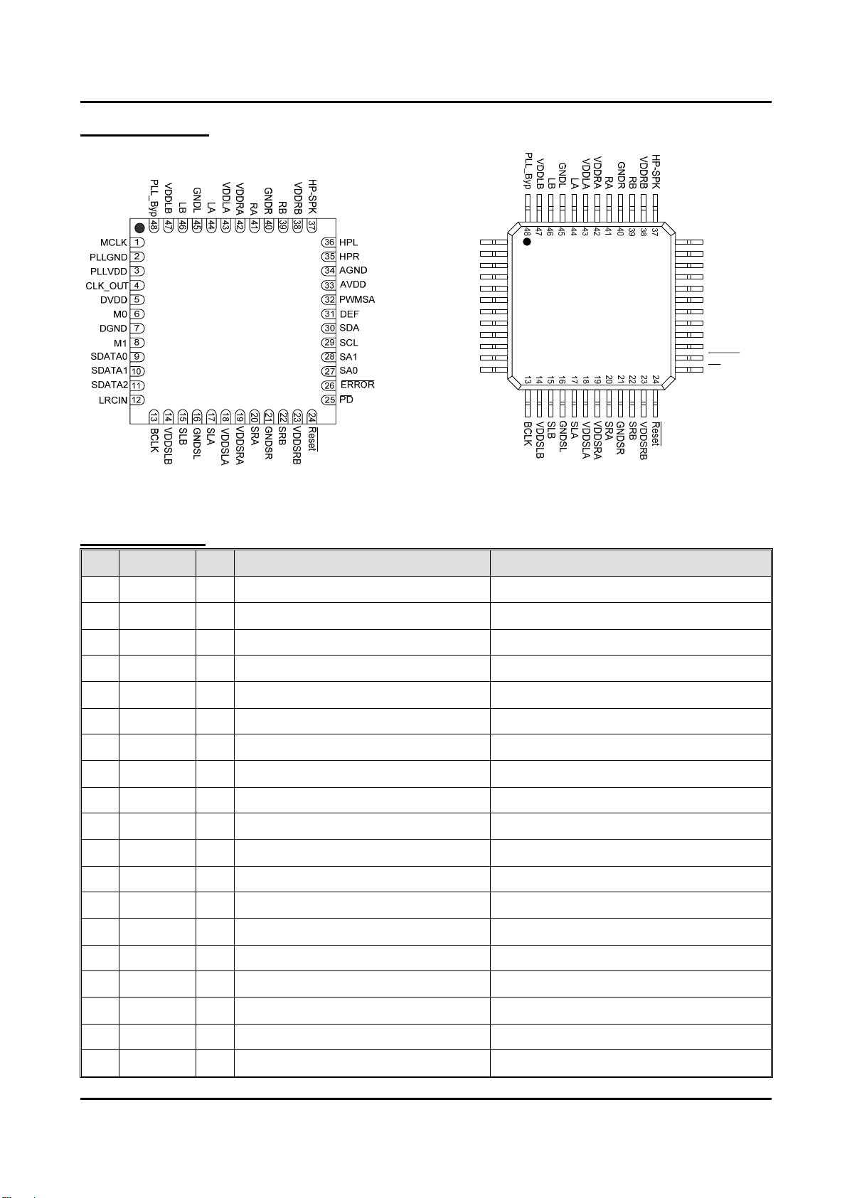
Pin Assignment
MCLK
PLLGND
PLLVDD
CLK_OUT
DVDD
MO
DGND
M1
SDATA0
SDATA1
SDATA2
LRCIN
1
2
3
4
5
6
7
8
9
10
11
12
36
35
34
33
32
31
30
29
28
27
26
25
Pin Description
PIN NAME
1 MCLK I Master clock input Schmitt trigger TTL input buffer
2 PLLGND P Ground for PLL
3 PLLVDD P Supply for PLL (Note1)
TYPE
DESCRIPTION CHARACTERISTICS
HPL
HPR
AGND
AVDD
PWMSA
DEF
SDA
SCL
SA1
SA0
ERROR
PD
4 CLK_OUT O PLL output TTL output buffer
5 DVDD P Digital Power (Note1)
6 M0 I Mode selection 0 Schmitt trigger TTL input buffer
7 DGND P Digital Ground
8 M1 I Mode selection 1 Schmitt trigger TTL input buffer
9 SDATA0 I Serial audio data input 0 Schmitt trigger TTL input buffer
10 SDATA1 I Serial audio data input 1 Schmitt trigger TTL input buffer
11 SDATA2 I Serial audio data input 2 Schmitt trigger TTL input buffer
12 LRCIN I Left/Right clock input (Fs) Schmitt trigger TTL input buffer
13 BCLK I Bit clock input (64Fs) Schmitt trigger TTL input buffer
14 VDDSLB P Supply for subwoofer-left channel B (Note2)
15 SLB O Subwoofer-left channel output (-)
16 GNDSL P Ground for subwoofer-left channel
17 SLA O Subwoofer-left channel output (+)
18 VDDSLA P Supply for subwoofer-left channel A (Note2)
19 VDDSRA P Supply for subwoofer-right channel A (Note2)
Elite Semiconductor Memory Technology Inc. Publication Date: May. 2007
Revision: 1.3 2/33
Page 3
ESMT AD8356A
20 SRA O Subwoofer-right channel output (+)
21 GNDSR P Ground for subwoofer-right channel
22 SRB O Subwoofer-right channel output (-)
23 VDDSRB P Supply for subwoofer-right channel B (Note2)
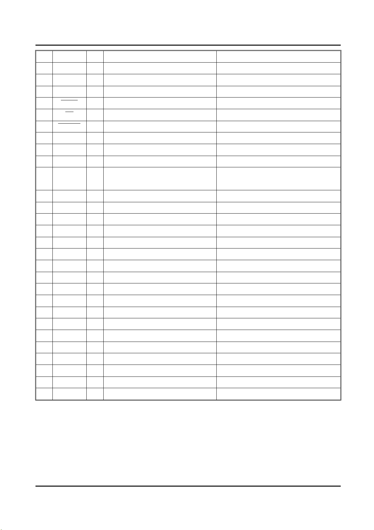
24
25
26
27 SA0 I I2C select address 0 Schmitt trigger TTL input buffer
28 SA1 I I2C select address 1 Schmitt trigger TTL input buffer
29 SCL I I2C serial clock input Schmitt trigger TTL input buffer
30 SDA I I2C serial data input
31 DEF I Default volume, 0=Mute, 1=Un-Mute Schmitt trigger TTL input buffer
32 PWMSA O Half-bridge, sub-woofer channel output TTL output buffer
33 AVDD P Analog supply (Note1)
34 AGND P Analog ground
35 HPR O Headphone right channel output
36 HPL O Headphone left channel output
37 HP-SPK I Headphone detection
38 VDDRB P Supply for right channel B (Note2)
setRe
PD
ERROR
I Reset, low active Schmitt trigger TTL input buffer
I Power down, low active Schmitt trigger TTL input buffer
O ERROR output Open-drain output
Schmitt trigger TTL input buffer with
open-drain output
39 RB O Right channel output (-)
40 GNDR P Ground for Right channel
41 RA O Right channel output (+)
42 VDDRA P Supply for right channel A (Note2)
43 VDDLA P Supply for left channel A (Note2)
44 LA O Left channel output (+)
45 GNDL P Ground for left channel
46 LB O Left channel output (-)
47 VDDLB P Supply for left channel B (Note2)
48 PLL_Byp I PLL Bypass Schmitt trigger TTL input buffer
Note1:These pins provide the supply for digital PWM controller, headphone drivers, built-in PLL and
protection circuits except for loudspeaker short-circuit protection circuits.
Note2:These pins provide the supply for loudspeaker driver stages, which are known as “PVDD”.
Elite Semiconductor Memory Technology Inc. Publication Date: May. 2007
Revision: 1.3 3/33
Page 4
ESMT AD8356A
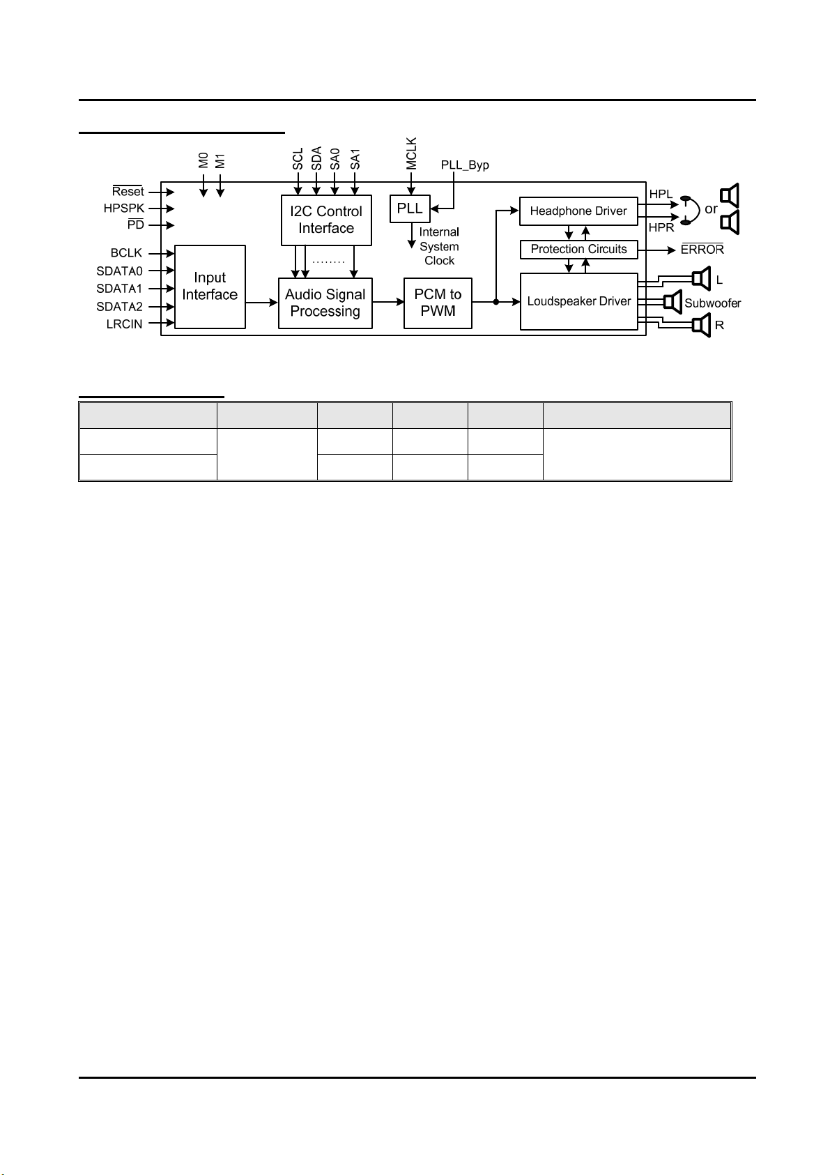
Functional Block Diagram
Available Package
Package Type Device No.
7x7 48L QFN 23.5 1.6 12.5
AD8356A
7x7 48L E-LQFP
Note3:The thermal pad is at the bottom of package. To optimize the performance of thermal dissipation,
solder the thermal pad to PCB’s ground plane is suggested.
θja(℃/W) Ψjt(℃/W) θjc(℃/W)
23.8 1.8 15.8
Exposed Thermal Pad
Yes (Note3)
Elite Semiconductor Memory Technology Inc. Publication Date: May. 2007
Revision: 1.3 4/33
 Loading...