

Page 1
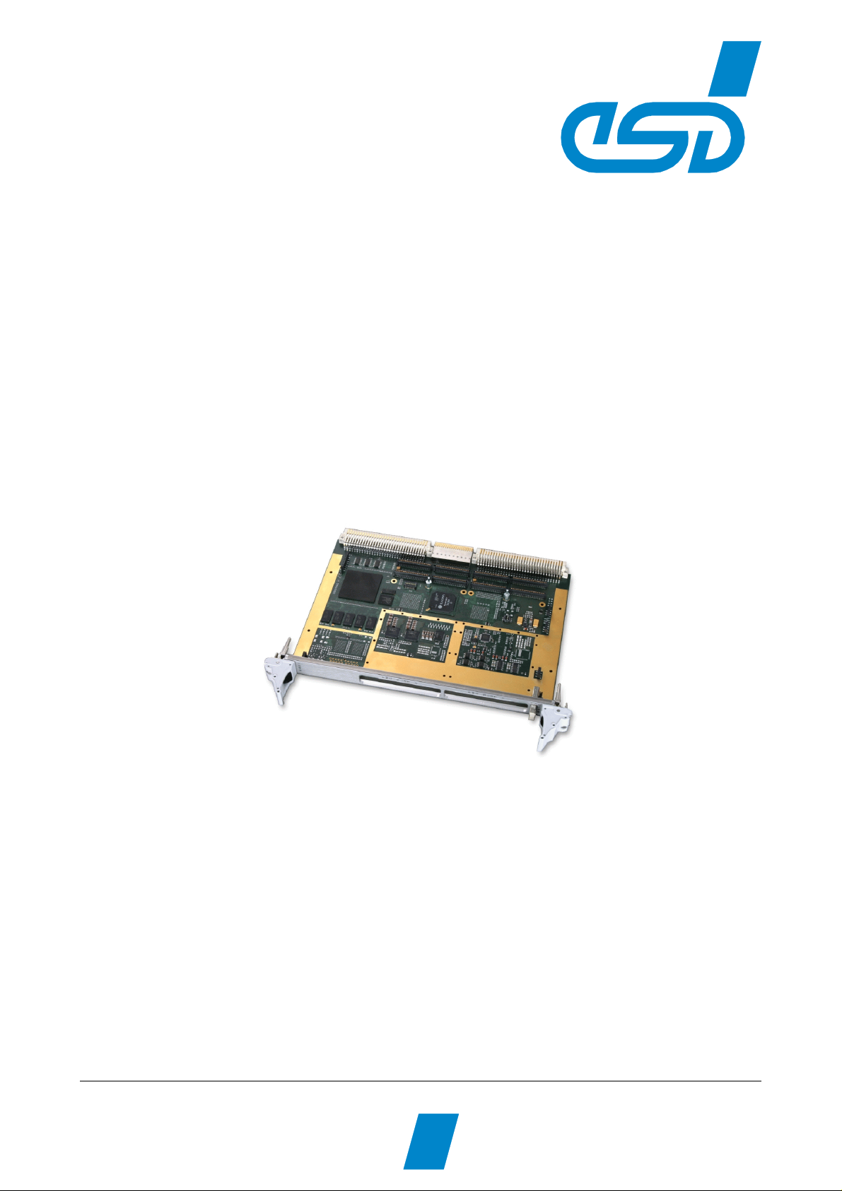
VME-PMC-CADDY/2
VME-Carrier Board
for PMC Modules
Hardware Manual
to Product:
V.1915.xx ,
V.1916.xx
VME-PMC-CADDY/2
esd electronic system design gmbh
Vahrenwalder Str. 207 • 30165 Hannover • Germany
http://www.esd.eu
Phone: +49 (0) 511 3 72 98-0 • Fax: +49 (0) 511 3 72 98-68
Hardware-Manual • Doc.-No.: V.1915.21 / Rev. 1.0
Page 1 of 43
Page 2

N O T E
The information in this document has been carefully checked and is believed to be entirely reliable. esd
makes no warranty of any kind with regard to the material in this document, and assumes no
responsibility for any errors that may appear in this document. esd reserves the right to make changes
without notice to this, or any of its products, to improve reliability, performance or design.
esd assumes no responsibility for the use of any circuitry other than circuitry which is part of a product
of esd gmbh.
esd does not convey to the purchaser of the product described herein any license under the patent rights
of esd gmbh nor the rights of others.
esd electronic system design gmbh
Vahrenwalder Str. 207
30165 Hannover
Germany
USA / Canada:
esd electronics Inc.
525 Bernardston Road
Suite 1
Greenfield, MA 01301
USA
Phone: +1-800-732-8006
Fax: +1-800-732-8093
E-mail: [email protected]
Internet: www.esd-electronics.us
Trademark Notices
CiA® and CANopen® are registered community trademarks of CAN in Automation e.V.
All other trademarks, product names, company names or company logos used in this manual are reserved by their respective
owners.
Page 2 of 43
Hardware Manual • Doc. No.: V.1915.21 / Rev. 1.0
VME-PMC-CADDY/2
Page 3
DocumentFile:
I:\Texte\Doku\MANUALS\VME\PMC-CADDY2\Englisch\VME-PMC-CADDY2_Manual_en_10.wpd
Date of print:
PCB version:
2012-02-01
VME-PMC-CADDY/2 Rev. 2.1
Changes in the chapters
The changes in the document listed below affect changes in the hardware and firmware as well as
changes in the description of facts only.
Chapter Changes versus previous version
1.0 First English version
Technical details are subject to change without further notice.
VME-PMC-CADDY/2
Hardware-Manual • Doc.-No.: V.1915.21 / Rev. 1.0
Page 3 of 43
Page 4
Safety Instructions
!
When working with VME-PMC-CADDY/2 modules follow the instructions below and read the
manual carefully to protect yourself and the VME-PMC-CADDY/2 module from damage.
!
Protect the VME-PMC-CADDY/2 module from dust, moisture and steam.
!
Protect the VME-PMC-CADDY/2 module from shocks and vibrations.
!
The VME-PMC-CADDY/2 module may become warm during normal use. Always allow adequate
ventilation around the VME-PMC-CADDY/2 module and use care when handling.
!
Do not operate the VME-PMC-CADDY/2 module adjacent to heat sources and do not expose it to
unnecessary thermal radiation. Ensure an ambient temperature as specified in the technical data.
!
Do not use damaged or defective cables to connect the VME-PMC-CADDY/2 module.
Qualified Personal
This documentation is directed exclusively towards qualified personal in control and automation engineering.
The installation and commissioning of the product may only be carried out by qualified personal, which is
authorized to put devices, systems and electric circuits into operation according to the applicable national
standards of safety engineering.
Intended Use
The intended use of the VME-PMC-CADDY/2 module is the operation as a carrier board in a VME-system.
The esd guarantee does not cover damages which result from improper use, usage not in accordance with
regulations or disregard of safety instructions and warnings.
!
The VME-PMC-CADDY/2 module is intended for installation in a VME-system only.
!
The operation of the VME-PMC-CADDY/2 module in hazardous areas, or areas exposed to
potentially explosive materials is not permitted.
!
The operation of the VME-PMC-CADDY/2 module for medical purposes is prohibited.
Service Note
The VME-PMC-CADDY/2 module does not contain any parts that require maintenance by the user. The VMEPMC-CADDY/2 module does not require any manual configuration of the hardware. Unauthorized intervention
in the device voids warranty claims. Remove all cables before cleaning. Clean the device with a slightly moist,
lint-free cloth. Cleaning agents or solvents are not suitable.
Disposal
Devices which have become defective in the long run have to be disposed in an appropriate way or have to be
returned to the manufacturer for proper disposal. Please, make a contribution to environmental protection.
Page 4 of 43
Hardware Manual • Doc. No.: V.1915.21 / Rev. 1.0
VME-PMC-CADDY/2
Page 5

Contents
1. Overview . . . . . . . . . . . . . . . . . . . . . . . . . . . . . . . . . . . . . . . . . . . . . . . . . . . . . . . . . . . . . . . . . . . . 6
1.1 Block Circuit Diagram . . . . . . . . . . . . . . . . . . . . . . . . . . . . . . . . . . . . . . . . . . . . . . . . . . . . . . 6
1.2 General . . . . . . . . . . . . . . . . . . . . . . . . . . . . . . . . . . . . . . . . . . . . . . . . . . . . . . . . . . . . . . . . . . 6
1.3 Characteristics of the Available Hardware Options . . . . . . . . . . . . . . . . . . . . . . . . . . . . . . . . 7
1.3.1 Option “-32P2”: Changed I/O-Pin Routing on P2 . . . . . . . . . . . . . . . . . . . . . . . . . . . . . 7
1.3.2 Option “-T”: Extended Temperature Range . . . . . . . . . . . . . . . . . . . . . . . . . . . . . . . . . 8
1.3.3 Option: “-CC”: Conduction Cooled . . . . . . . . . . . . . . . . . . . . . . . . . . . . . . . . . . . . . . . 8
1.4 Technical Data . . . . . . . . . . . . . . . . . . . . . . . . . . . . . . . . . . . . . . . . . . . . . . . . . . . . . . . . . . . . 9
1.4.1 General Technical Data . . . . . . . . . . . . . . . . . . . . . . . . . . . . . . . . . . . . . . . . . . . . . . . . . 9
1.4.2 Serial Interfaces . . . . . . . . . . . . . . . . . . . . . . . . . . . . . . . . . . . . . . . . . . . . . . . . . . . . . . 10
1.4.3 PMC-Slots . . . . . . . . . . . . . . . . . . . . . . . . . . . . . . . . . . . . . . . . . . . . . . . . . . . . . . . . . . 11
1.4.4 XMC Slot (Option) . . . . . . . . . . . . . . . . . . . . . . . . . . . . . . . . . . . . . . . . . . . . . . . . . . . 12
1.4.5 Software . . . . . . . . . . . . . . . . . . . . . . . . . . . . . . . . . . . . . . . . . . . . . . . . . . . . . . . . . . . . 12
2. Front Panel and LEDs . . . . . . . . . . . . . . . . . . . . . . . . . . . . . . . . . . . . . . . . . . . . . . . . . . . . . . . . 13
2.1 LED Display . . . . . . . . . . . . . . . . . . . . . . . . . . . . . . . . . . . . . . . . . . . . . . . . . . . . . . . . . . . . . 15
2.2 Reset Button . . . . . . . . . . . . . . . . . . . . . . . . . . . . . . . . . . . . . . . . . . . . . . . . . . . . . . . . . . . . . 15
3. PCB View with Coding Switches and Connectors . . . . . . . . . . . . . . . . . . . . . . . . . . . . . . . . . 16
3.1 Default Setting of the Coding Switches . . . . . . . . . . . . . . . . . . . . . . . . . . . . . . . . . . . . . . . . 17
3.2 VMEbus Configuration (SW600) . . . . . . . . . . . . . . . . . . . . . . . . . . . . . . . . . . . . . . . . . . . . 18
3.2.1 Overview . . . . . . . . . . . . . . . . . . . . . . . . . . . . . . . . . . . . . . . . . . . . . . . . . . . . . . . . . . . 18
3.2.2 VMEbus System Controller Setup . . . . . . . . . . . . . . . . . . . . . . . . . . . . . . . . . . . . . . . . 19
3.2.3 VMEbus Power-Up-Options . . . . . . . . . . . . . . . . . . . . . . . . . . . . . . . . . . . . . . . . . . . . 20
3.3 PMC Slot Configuration (SW800) . . . . . . . . . . . . . . . . . . . . . . . . . . . . . . . . . . . . . . . . . . . . 21
4. Address Assignment of VME-PMC-CADDY/2 . . . . . . . . . . . . . . . . . . . . . . . . . . . . . . . . . . . . 22
5. Connector Assignment . . . . . . . . . . . . . . . . . . . . . . . . . . . . . . . . . . . . . . . . . . . . . . . . . . . . . . . . 23
5.1 Serial Interfaces RS232 (X1940) . . . . . . . . . . . . . . . . . . . . . . . . . . . . . . . . . . . . . . . . . . . . . 23
5.2 Adapter Cable “VME-PMC-CPU/Cable” . . . . . . . . . . . . . . . . . . . . . . . . . . . . . . . . . . . . . . 24
5.3 Adapter Cable “VME-PMC-CPU/Cable-Y” . . . . . . . . . . . . . . . . . . . . . . . . . . . . . . . . . . . . 25
5.4 VMEbus P1 . . . . . . . . . . . . . . . . . . . . . . . . . . . . . . . . . . . . . . . . . . . . . . . . . . . . . . . . . . . . . 26
5.5 Standard Assignment of I/O-Signals . . . . . . . . . . . . . . . . . . . . . . . . . . . . . . . . . . . . . . . . . . 27
5.5.1 Standard Assignment VMEbus P2 (According to VITA 35, P4 V2-64ac) . . . . . . . . . 27
5.5.2 Standard Assignment of Transfer Module with P2 Row a and c Signals . . . . . . . . . . 28
5.5.3 Standard Assignment VMEbus P0 . . . . . . . . . . . . . . . . . . . . . . . . . . . . . . . . . . . . . . . 29
5.5.4 Standard Assignment of the I/O Connector J14 at PMC Slot 1 . . . . . . . . . . . . . . . . . 30
5.5.5 Standard Assignment of the I/O Connector J24 at PMC Slot 2 . . . . . . . . . . . . . . . . . 31
5.6 Assignment of the I/O-Signals using the‘-32P2’ Option . . . . . . . . . . . . . . . . . . . . . . . . . . . 32
5.6.1 Assignment VMEbus P2 using ‘-32P2’ Option . . . . . . . . . . . . . . . . . . . . . . . . . . . . . 32
5.6.2 Assignment of a Transfer Module at ‘-32P2’ Option . . . . . . . . . . . . . . . . . . . . . . . . . 33
5.6.3 Assignment VMEbus P0 at ‘-32P2’ Option . . . . . . . . . . . . . . . . . . . . . . . . . . . . . . . . 34
5.6.4 Assignment of the PMC Connector J14 at ‘-32P2’ Option . . . . . . . . . . . . . . . . . . . . . 35
5.6.5 Assignment of the PMC Connector J24 at ‘-32P2’ Option . . . . . . . . . . . . . . . . . . . . . 36
5.7 Special Assembly: J24-I/O-Signals to d+z of P2 (acc. VITA 35, P4 V2-46dz) . . . . . . . . . . 37
5.7.1 Assignment of P2 at Special Assembly with RC800, RC801, ...RC811 . . . . . . . . . . . 37
5.7.2 Assignment I/O Connector J24 at Assembly with RC800, RC801, ...RC811 . . . . . . . 38
5.8 XMC Socket J15 (Option) . . . . . . . . . . . . . . . . . . . . . . . . . . . . . . . . . . . . . . . . . . . . . . . . . . 39
6. References . . . . . . . . . . . . . . . . . . . . . . . . . . . . . . . . . . . . . . . . . . . . . . . . . . . . . . . . . . . . . . . . . . 41
7. Order Information . . . . . . . . . . . . . . . . . . . . . . . . . . . . . . . . . . . . . . . . . . . . . . . . . . . . . . . . . . . 42
VME-PMC-CADDY/2
Hardware-Manual • Doc.-No.: V.1915.21 / Rev. 1.0
Page 5 of 43
Page 6

Overview
1. Overview
1.1 Block Circuit Diagram
XMC-
Option
2eSST
s
u
b
E
M
V
1
P
s
u
b
E
M
V
2
P
VME
Address
Driver
VME
Control Logic
VME
Data
Driver
VME
Address
Driver
VME
Control Logic
VME
Data
Driver
VME PCI
Bridge
Tundra
Tsi148
64 bit at 66 MHz PCI bus
Flash
DDR2
PEX
PCI
Freescale
MPC 8349
PMC Add On
Connectors
J11 J12
J13
J21 J22
J23
2x Serial
Interface
RS-232
PMC Module
J15
Slot 1
XMC
J14
PMC Module
Slot 2
J24
Only at VME-PMC-CADDY/2 versions (order no. V.1915.xx)
P2 I/O Signals to
PMC Module 1 / J14
(Standard Routing:
P4V2-64ac acc. to
ANSI/VITA 35)
O
/
I
2
P
P0 I/O Signals to
PMC Module 2 / J24
(Standard Routing:
P4V0-64 acc. to
O
ANSI/VITA 35)
/
I
0
P
2x RS-232 Interface
HARLINK10
Figure 1: Block circuit diagram of VME-PMC-CADDY/2
1.2 General
The VMEbus unit VME-PMC-CADDY/2 is a VME64-base board which can carry up to two PMC
modules of normal size. For the VMEbus connection the VME-PCI bridge Tsi148 by Tundra is used.
The Tsi148 is designed in a way that the board can either operate as slave or as master on the VMEbus.
If the board operates as master, it supports a 4-level arbiter.
The VMEbus interrupt can be applied to any of the seven interrupt-request lines. The VME-PMCCADDY/2 is connected to the VMEbus by two 160-pin VG-connectors (complementary to DIN41612)
for VME64 systems.
An active VMEbus-interrupt request is indicated by a red LED and a VMEbus access onto the board
is indicated by a yellow LEDs in the front panel (not in Conduction Cooled version)
Both PMC slots are designed according to the standard IEEE Std 1386-2001 (except the standard I/O
pin routing). It is possible therefore to insert all PMC modules, that use 3.3 V signalling only.
In addition to the connectors for the PMC-address/data and control signals, every slot of the
VME-PMC-CADDY/2 has an I/O-connector which applies the I/O-signals of the PMC modules to
VMEbus connector P2.
Two different P2 pin assignments are available: In the standard configuration each P2-pin is only
connected to one I/O-pin of the PMC-modules acc. to VITA 35 (P4V2-64ac, P4V0-64).
In the option ‘-32P' the pin assignment is designed acc. to IEEE Std 1386-2001, Table 8. This pin
Page 6 of 43
Hardware Manual • Doc. No.: V.1915.21 / Rev. 1.0
VME-PMC-CADDY/2
Page 7

Overview
assignment offers the connection of the two PMC-modules via P2, because several PMC-I/O-signals
are shorted at P2.
The front panel of the VME-PMC-CADDY/2 has two cutouts for the front panels of the PMC modules.
A blank cover for unused slots is included in the price.
Example libraries for the initialization of the board in C source code for VxWorks is available for a fee
on a disk (MS-DOS format). Drivers for other operating systems are available on request. Please state
your operating system with the version number when you order.
1.3 Characteristics of the Available Hardware Options
Note: All options given below have to be specified when ordering. They can not be installed later. For
an overview of the possible combinations of the options see page 42.
1.3.1 Option “-32P2”: Changed I/O-Pin Routing on P2
The VME-PMC-CADDY/2 is currently available with two different I/O-pin assignments:
- In the Standard configuration each of the I/O-pins of the PMC slot 1 (J14) is connected to exactly
one pin of the VMEbus connector P2 (according to VITA 35 (P4V2-64ac)) and each of the I/O-pins
of the PMC slot 2 (J24) is connected with exactly one I/O-pin of the VMEbus connector P0
(according to VITA 35 (P4V0-64)) .
- In the VME-PMC-CADDY/2 with the option “-32P”the pins are assigned according to IEEE
Std.1386-2001, Table 8. In this option the I/O-signals of both PMC-slots are connected with the pin
rows a+c of the VME-connector P2:
The pins 33...64 of the PMC-connector J24 are connected in parallel to this also to the rows
a and c of the P2 connector. This leads to a double assignment of the pins a1..a16 and c1...c16
on P2. Furthermore by this both PMC slots are connected with each other via 32 of their I/Opins.
Advantage: Access via a Standard-VMEbus-P2-I/O-adapter to each the half of the I/O-signals
of both PMC slots.
Disadvantage: You have to pay attention that your choice of inserted PMC modules does not
lead to undesired interactions between the modules, due to the I/O-signal
connection between the slots!
VME-PMC-CADDY/2
Hardware-Manual • Doc.-No.: V.1915.21 / Rev. 1.0
Page 7 of 43
Page 8
Overview
1.3.2 Option “-T”: Extended Temperature Range
The VME-PMC-CADDY/2 with this option is designed for the operation in the extended temperature
range of -40 /C ...+85 /C.
1.3.3 Option: “-CC”: Conduction Cooled
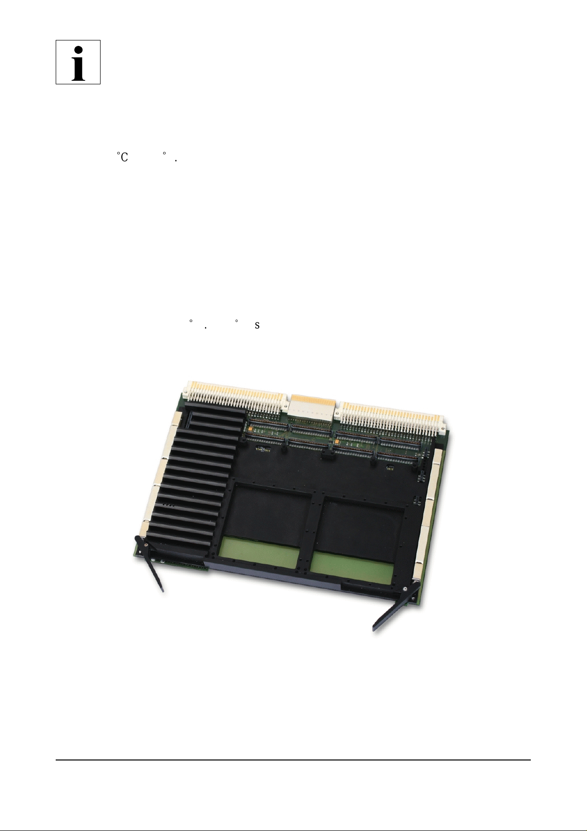
The VME-PMC-CADDY/2-CC is designed with covering heat sinks for heat dissipation in conduction
cooled systems. The slots of the PMC modules are conduction cooled PMC modules.
As a result of the heat sinks the front panel and with it the 10-pin har-link®-connector with the serial
interfaces are not equipped. Furthermore the front panel LEDs are not equipped.
The conduction cooled version VME-PMC-CADDY/2-CC is designed for operation in the extended
temperature range from -40 /C ...+85 /C as the VME-PMC-CADDY/2-T version.
Page 8 of 43
Figure 2: Conduction cooled version VME-PMC-CADDY/2-CC
Hardware Manual • Doc. No.: V.1915.21 / Rev. 1.0
VME-PMC-CADDY/2
Page 9
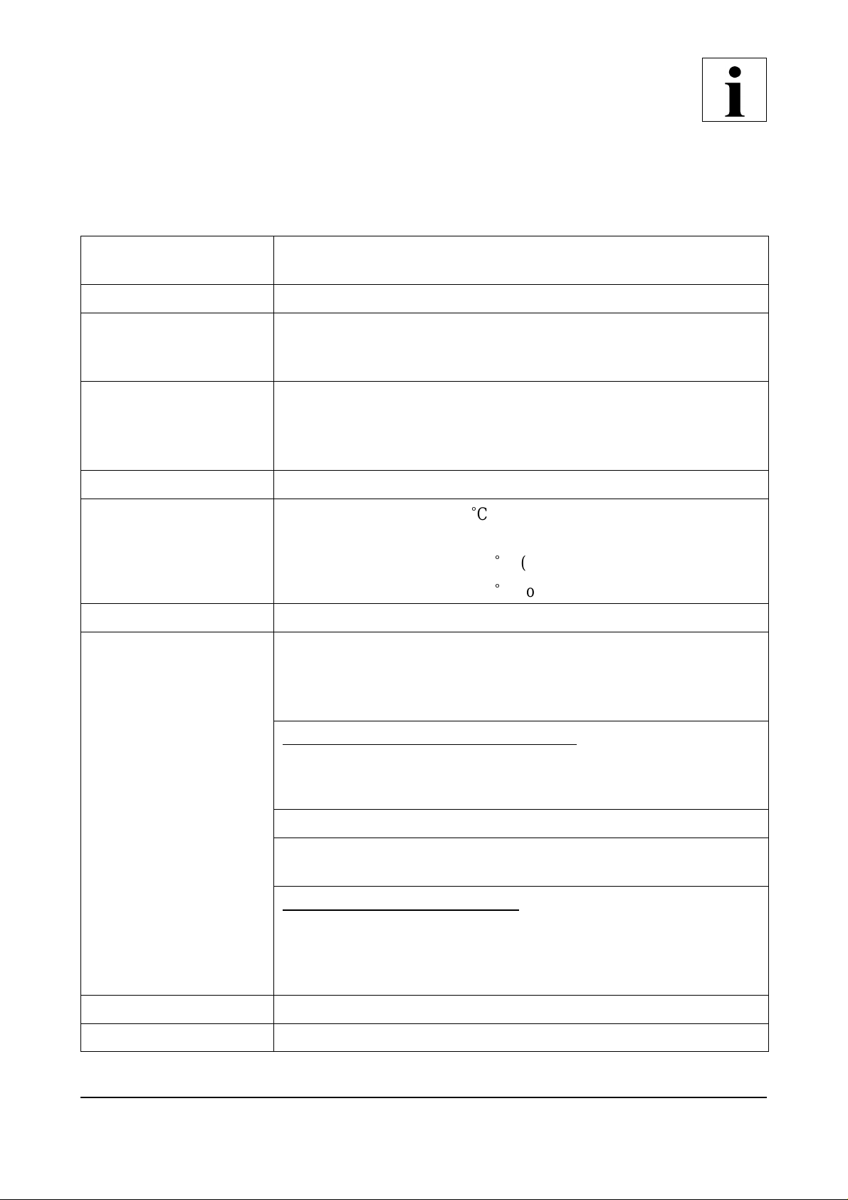
1.4 Technical Data
1.4.1 General Technical Data
Overview
VMEbus-Interface
Base address geographical addressing
Address modifier
VMEbus access
VMEbus back plane compatible to VME32, VME64 and VME64x back planes
Ambient temperature
range
Humidity max. 90%, non-condensing
IEEE 1014 / Rev. D
Master or Slave functionality
standard supervisory and non-privileged data access,
extended supervisory and non-privileged data access,
short supervisory and non-privileged access
- Legacy-protocols supporting the preservation of existing VMEsystems
- VME64 extensions
- 2eVME- and 2eSST protocols
Standard: 0...50 /C (order no.: V.1915.02/.11)
Extended
temperature range: -40...+85 /C (order no.: V.1915.03 /.13)
Conduction cooled: -40...+85 /C (order no.: V.1916.02 /.11)
P1, P2 - 160-pin VG-connector according to DIN 41612
in compliance with VME64 extension
P0 - 95-pin I/O-connector according to
IEC 1076-4-101
J11 to J24 - 64-pin PMC-socket connector:
J11, J12, J21, J22 - PMC-address/data signals
J13, J23 - PCI 64 signals
J14, J24 - PMC I/O-signals
Connectors
Dimensions 160 mm x 233 mm
Slot format 6 U high / 4 HP wide
VME-PMC-CADDY/2
J15 - 114-pin XMC socket (optional)
X1940 - 10-pin har-link socket: 2x serial (RS232)
Service- and diagnostic connector:
X1800 - Socket connector 1x16: Debug CPU
X1801 - Socket connector 1x7: JTAG-TSI148
X2120 - Socket connector 1x7: JTAG-PCI
X2310 - Socket connector 1x6: ISP-ADU848
Hardware-Manual • Doc.-No.: V.1915.21 / Rev. 1.0
(not at VME-PMC-CADDY/2-CC)
Page 9 of 43
Page 10
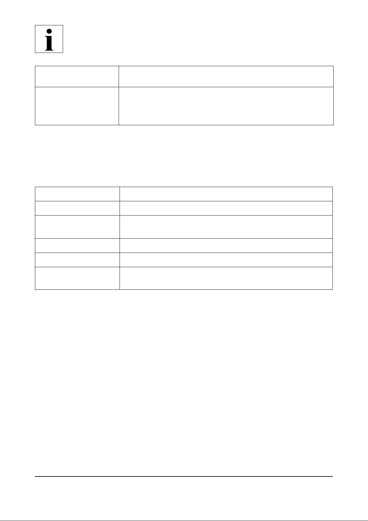
Overview
Weight
VME-PMC-CADDY/2 (order no.: V.1915.xx): 350 g
VME-PMC-CADDY/2-CC (order no.: V.1916.xx): 650 g
VMEbus P1, P2: 5 V ±5% / ca. 1,0 A
Power supply voltage
(without PMC modules)
Table 1: General technical data
1.4.2 Serial Interfaces
Number 2
Control UART im MPC8349
Signals
to X1940: RxD, TxD, RTS, CTS (for each port)
to VMEbus P0: RxD, TxD (for each port)
Bit rate 300 bit/s ... 115.200 bit/s
3.3 V ±5% / ca. 400 mA
+12V ±5% (only to PMC slots)
-12V ±5% (only to PMC slots)
Physical interface RS232
Connector
X1940 (10-pin har-link) and VMEbus P0,
Adapter cable 10-pol har-link to 9-pin DSUB available
Table 2: Serial interfaces
Page 10 of 43
Hardware Manual • Doc. No.: V.1915.21 / Rev. 1.0
VME-PMC-CADDY/2
Page 11
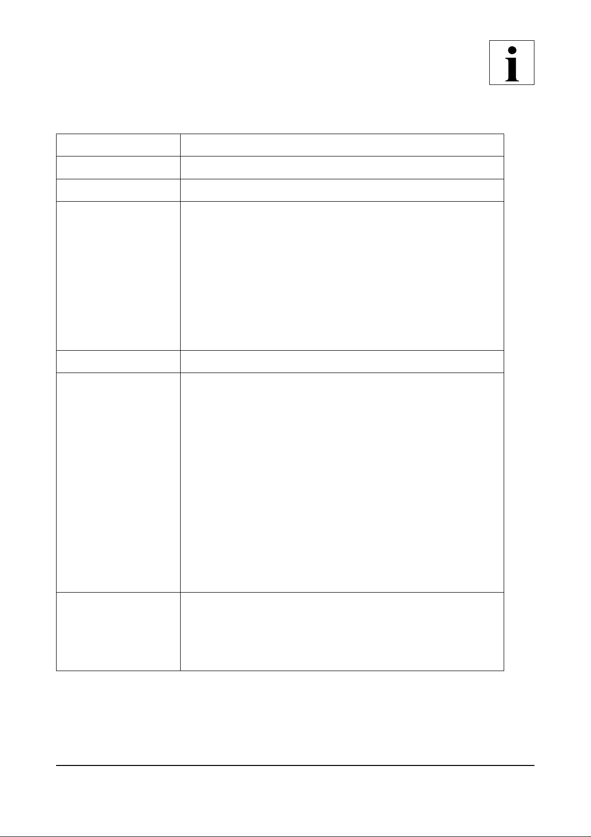
1.4.3 PMC-Slots
PMC-Standard IEEE Std 1386-2001, IEEE Std 1386.1-2001
Equipment two single-size modules
VME-PCI-Bridge Tundra Tsi148
Standard: according to VITA 35 (P4V2-64ac, P4V0-46), i.e.
PMC slot 1 (J14) completely to P2 row a and c,
PMC slot 2 (J24) completely to VMEbus connector
P0
I/O-Signals
to VMEbus P2 and P0
Option ‘-32P2’:
PMC slot 1 (J14): as above but additionally on P2
parallel assignment with J24 pins 33...64,
PMC slot 2 (J24): as above but additionally on P0
parallel assignment with J14-pins 1...32
Overview
Signal voltage level 3.3 V
In the standard placement all PMC-power supply voltages are
directly suppled via the VMEbus connectors.
3.3 V: max. 1.5 A current consumption per PMC slot
3.3 V AUX: for both PMC slots together
Power supply voltage
+12V: max. 1.0 A current consumption per PMC slot
-12V: max. 1.0 A current consumption per PMC slot
Note:
The maximum permissible sum of the power consumption of a
PMC module corresponds to the value of 15 W for double-sided
modules defined in the IEEE Std. 1386-2001.
3.3 V power supply voltage of the PMC modules generated from
Option for power
supply voltage
+5V-power supply voltage of the VMEbus (Necessary, if
VMEbus-back plane connector J1 is not of 160-pin design or no
3.3 V voltage is supplied via the VMEbus.)
Please contact our support before you order this version.
max. 250 mA current consumption
VME-PMC-CADDY/2
Table 3: PMC slots
Hardware-Manual • Doc.-No.: V.1915.21 / Rev. 1.0
Page 11 of 43
Page 12

Overview
1.4.4 XMC Slot (Option)*
VITA 42.3,
XMC standard
Link-definition according to table 4-1: Single width, 4-Lane, only
connector P15 is used
Bus system PCI-Express
Connector Connector assignment according to VITA 42.3, table 4-2
U
= 5V ±5 % (max. 1.0 A current consumption)
VPWR
(alternatively, adjustable via solder bridges U
U
= 3.3 V ±0,3V (max. 1.0 A current consumption)
3.3V
Power supply voltage
U
U
U
= 3.3 V ±0,3V (max. 1.0 A current consumption)
3.3VAUX
= +12 V ±5 % (max. 1.0 A current consumption)
+12V
= -12 V ±5 % (max. 1.0 A current consumption)
-12V
= 12V ±5%)
VPWR
Note:
The maximum permissible sum of the power consumption of the
XMC-module corresponds to the value of 15 W for double-sided
PMC-modules defined in IEEE Std. 1386-2001
* At the moment for this assembly variant there is no order option. If you need this hardware variant, please contact our
sales team ([email protected]) before ordering.
1.4.5 Software
Example libraries for the initialisation of the VME-PMC-CADDY/2 in C-code for VxWorks are
available for a fee. Ask our support for drivers for other operating systems.
Please specify your operating system with release number when ordering.
Page 12 of 43
Hardware Manual • Doc. No.: V.1915.21 / Rev. 1.0
VME-PMC-CADDY/2
Page 13
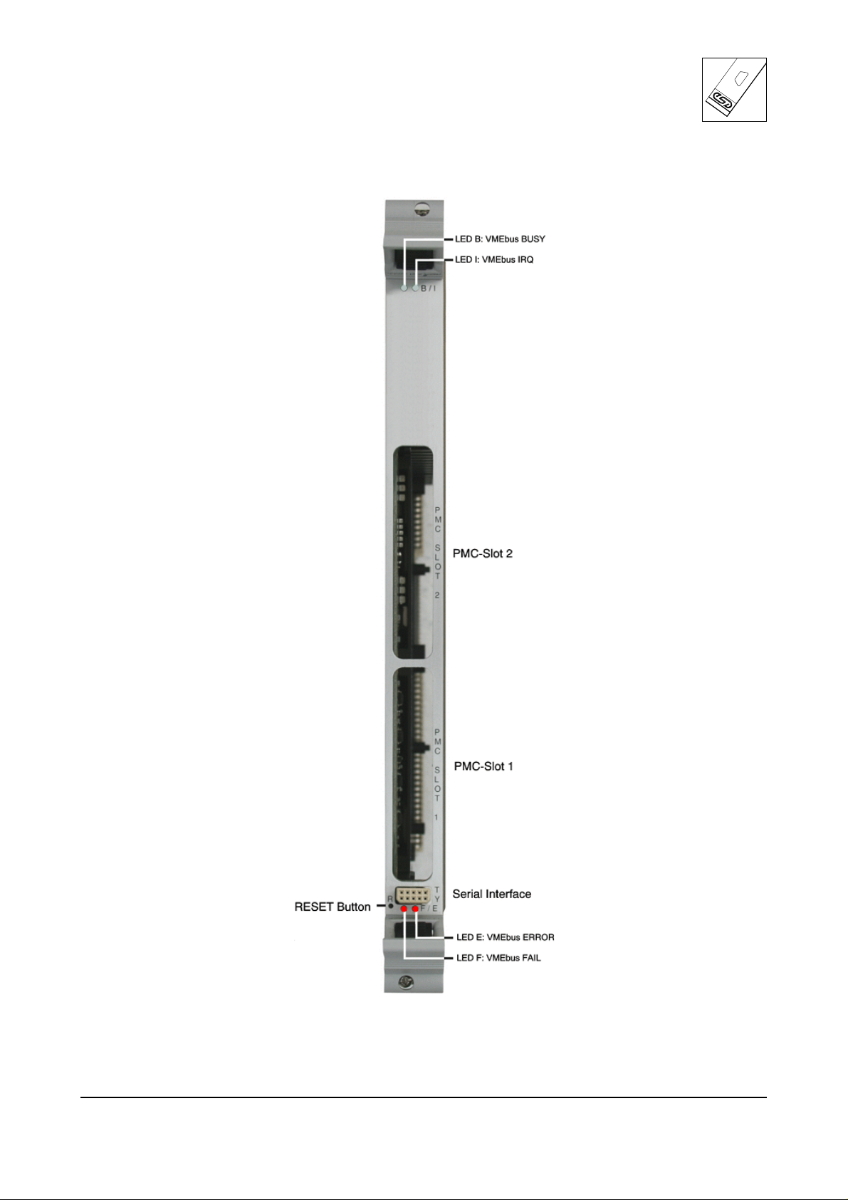
2. Front Panel and LEDs
Front Panel and LEDs
VME-PMC-CADDY/2
Figure 3: Front of the VME-PMC-CADDY/2
Hardware-Manual • Doc.-No.: V.1915.21 / Rev. 1.0
Page 13 of 43
Page 14
Front Panel and LEDs
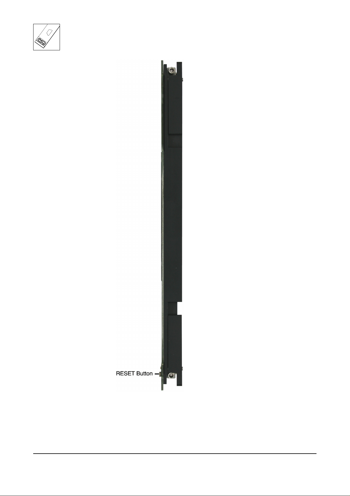
Figure 4: Front of the conduction cooled version VME-PMC-CADDY/2-CC
Page 14 of 43
Hardware Manual • Doc. No.: V.1915.21 / Rev. 1.0
VME-PMC-CADDY/2
Page 15
2.1 LED Display
LED
Front Panel and LEDs
Labelling on
front panel
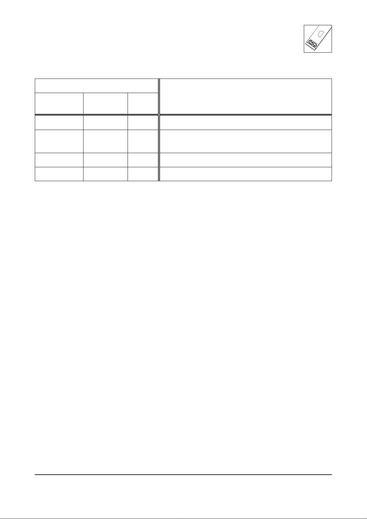
B BUSY green Access from VMEbus to VME-PMC-CADDY/2
I IRQ green
F FAIL red VME-PMC-CADDY/2 triggers FAIL on VMEbus
E BERR red VME-PMC-CADDY/2 triggers Bus-Error on VMEbus
Name Colour
VME-PMC-CADDY/2 triggers an interrupt on the
VMEbus
Table 4: Indication of the LEDs
Meaning (LED on)
2.2 Reset Button
The reset button can be enabled by pushing with a non-conducting bar-shaped object (max. 1.5 mm
diameter).
It triggers a local reset on the VME-PMC-CADDY/2 and consequently also on the PMC modules.
Furthermore a reset is triggered on the VMEbus.
VME-PMC-CADDY/2
Hardware-Manual • Doc.-No.: V.1915.21 / Rev. 1.0
Page 15 of 43
Page 16
Configuration
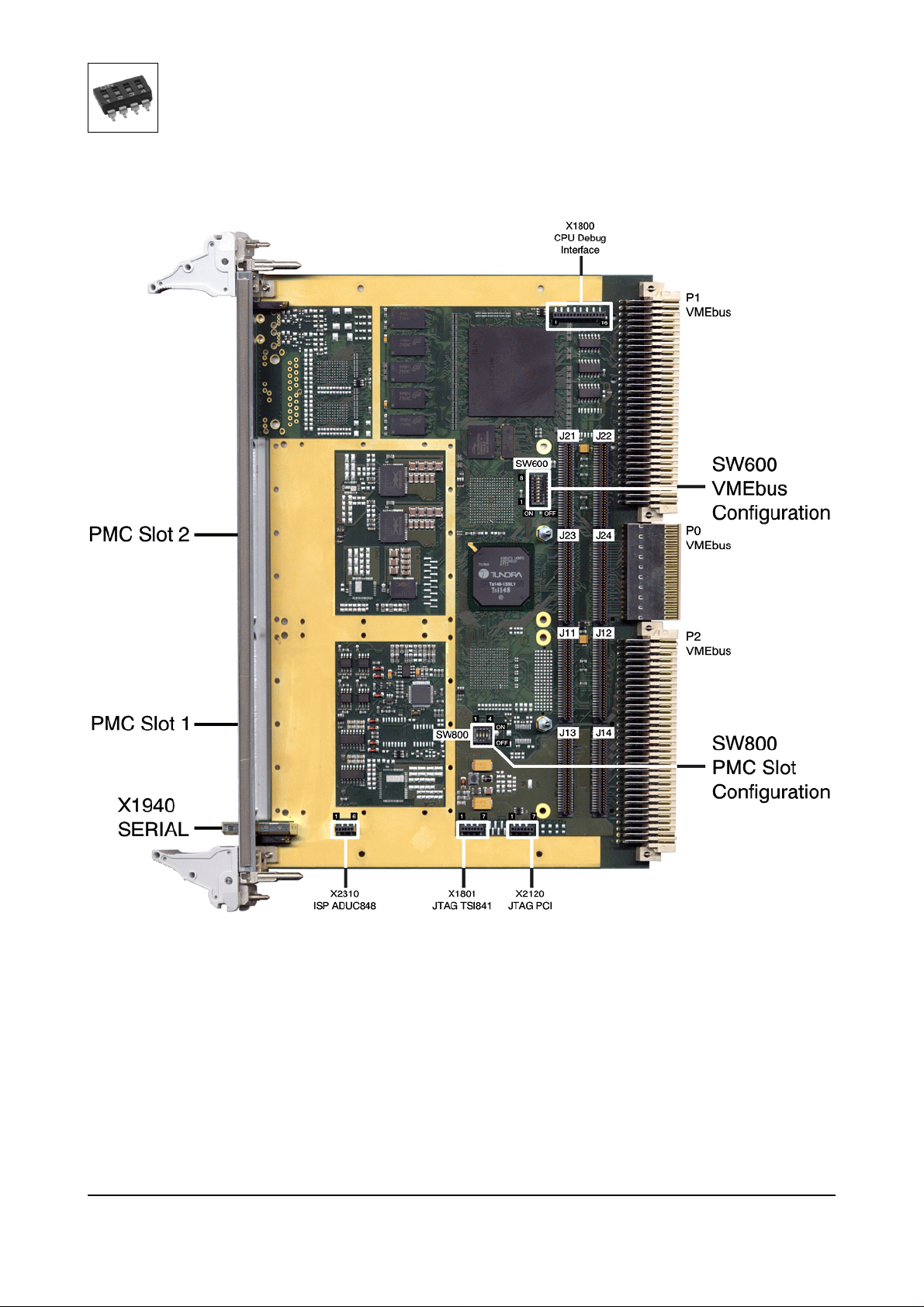
3. PCB View with Coding Switches and Connectors
Figure 5: Position of the coding switches and connectors on VME-PMC-CADDY/2
Page 16 of 43
Hardware Manual • Doc. No.: V.1915.21 / Rev. 1.0
VME-PMC-CADDY/2
Page 17
Configuration
3.1 Default Setting of the Coding Switches
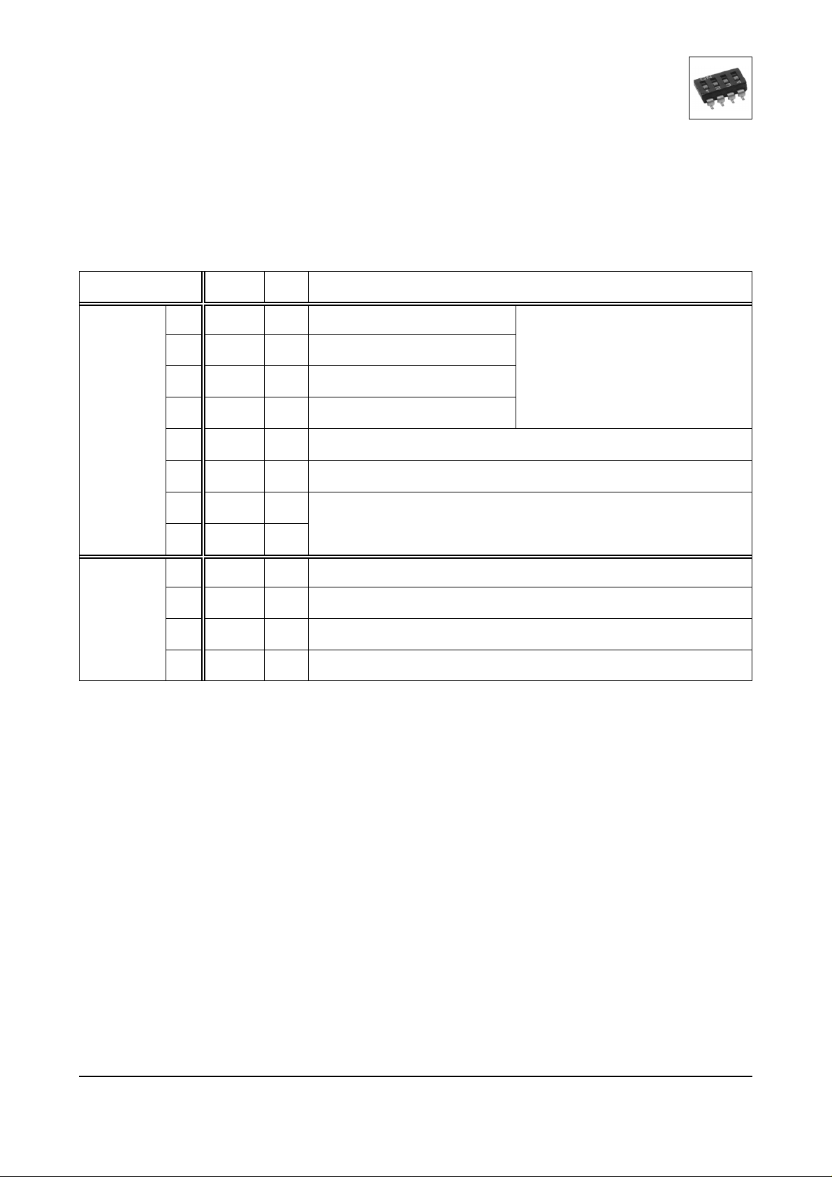
The default settings of the board as delivered is shown in the following table.
The position of the coding switch can be taken from figure 5. In the following description they are
shown as if the board is viewed with the VMEbus connectors on the right (view from PMC slot side).
Coding switch Setting Value Description
8 OFF 1
7 OFF 1
6 ON 0
5 ON 0
SFAILEN Control Bit Reset Value
SFAILAI Control Bit Auto Clear
Auto Slot ID Enable
Geographical Slot ID Enable
SW600
4 OFF 1 not used
3 OFF 1 not used
2 OFF 1
1 ON 0
VMEbus System Controller:
Default: System Controller Function disabled
4 OFF 1 PMC module 1 is not configured as Monarch
3 OFF 1 PMC module 2 is not configured as Monarch
SW800
2 ON 0 PCI-Bus of the PMC module is set to the fixed value of 33 MHz
1 OFF 1 (PUPEN) reserved for future applications
*) For details on the evaluation of the bits see [1].
VMEbus Power Up Options
Table 5: Overview of the default setting of the coding switches
VME-PMC-CADDY/2
Hardware-Manual • Doc.-No.: V.1915.21 / Rev. 1.0
Page 17 of 43
Page 18
Configuration
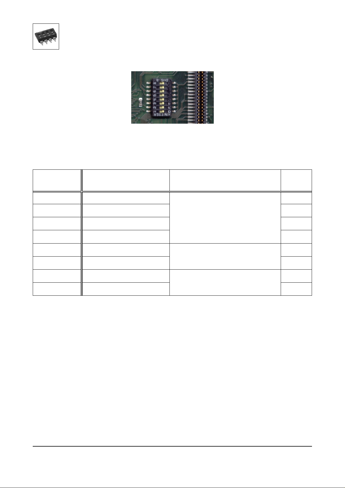
3.2 VMEbus Configuration (SW600)
Figure 6: Coding Switch SW600
3.2.1 Overview
Coding switch
contact
8
7
6
5
SFAILEN Control Bit Reset Value
SFAILAI Control Bit Auto Clear
Auto Slot ID Enable
Geographical Slot ID Enable
4 not used
3 not used OFF
2 SCONEN#
1 SCONDIS# ON
Table 6: Assignment of the coding switch SW600
Value of the parameter bits:
ON: Bit = ‘0’
OFF: Bit = ‘1’
Bit name Function
VMEbus Power Up Optionen
these coding switches are not
evaluated
VMEbus System Controller Setup
Default
setting
OFF
OFF
ON
ON
OFF
OFF
Page 18 of 43
Hardware Manual • Doc. No.: V.1915.21 / Rev. 1.0
VME-PMC-CADDY/2
Page 19
Configuration
3.2.2 VMEbus System Controller Setup
This bits define how and whether the VME-PMC-CADDY/2 is activated as VMEbus system controller.
Coding switch-
contact 2
Coding switch
contact 1
Function
SCONEN# SCONDIS#
OFF OFF
Auto SCON: automatic activation of the system
controller (depending of signal VBG3IN#))
ON OFF System controller activated
OFF ON System controller deactivated
ON ON not allowed
Table 7: VMEbus system controller activation
Value of the parameter bits:
ON: Bit = ‘0’
OFF: Bit = ‘1’
Please refer to chapter “5.4.3 System Controller (SCON)” in the manual of the Tundra PCI/X-toVMEbus bridge TS148 [1] for details about the system controller functions.
VME-PMC-CADDY/2
Hardware-Manual • Doc.-No.: V.1915.21 / Rev. 1.0
Page 19 of 43
Page 20
Configuration
3.2.3 VMEbus Power-Up-Options
After a reset the Tundra PCI/X-to-VMEbus-bridge TS148 evaluates different PCI/X-bus and VMEbus
signals to enable or disable various functions. For the VMEbus the data signals VD[0] to VD[3] are
evaluated.
Coding switch
contact
VMEbus
data bit
Power-up option Description
8 VD[0] SFAILEN_RV SFAILEN Control Bit Reset Value
7 VD[1] SFAILAI_AC SFAILAI Control Bit Auto Clear
5 VD[2] ASIDEN Auto Slot ID Enable
6 VD[3] GSIDEN Geographical Slot ID Enable
Table 8: VMEbus-Power-Up option bits
Please, refer to chapter “5.4.2 VMEbus Power-up Options” in the manual of the Tundra PCI/X-toVMEbus-Bridge TS148 [1] for details about the comprehensive VMEbus Power-Up options.
Page 20 of 43
Hardware Manual • Doc. No.: V.1915.21 / Rev. 1.0
VME-PMC-CADDY/2
Page 21
3.3 PMC Slot Configuration (SW800)
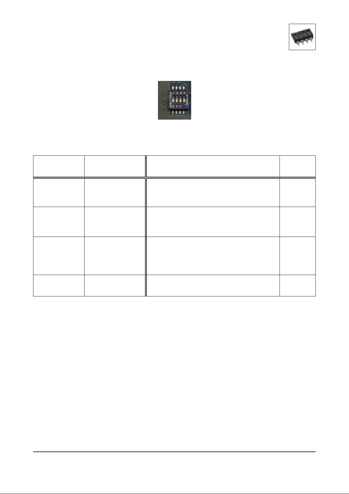
Figure 7: Coding switch SW800
Configuration
Coding switch-
contact
4 P-MONARCH 1#
3 P-MONARCH 2#
2 P-M66EN
1 P-PUPEN
Name Description Default
Monarch/Non-Monarch PMC module 1
OFF: Non-Monarch
OFF
ON: Monarch
Monarch/Non-Monarch PMC module 2
OFF: Non-Monarch
OFF
ON: Monarch
Clock rate of the PCI-Bus of the PMC
modules:
OFF: 66 MHz
ON
ON: 33 MHz
reserved for future applications;
always set to “OFF”
OFF
Table 9: PMC slot configuration via SW800
VME-PMC-CADDY/2
Hardware-Manual • Doc.-No.: V.1915.21 / Rev. 1.0
Page 21 of 43
Page 22
Address Assignment
4. Address Assignment of VME-PMC-CADDY/2
Address range Assignment
0x00000000
0x80000000
0x90000000
0xe0000000
0xe2000000
0xffc00000
0x07ffffff
...
0x8fffffff
...
0x9fffffff
...
0xe00fffff
...
0xe20fffff
...
0xffffffff
...
DDR2 RAM (72 bit data width)
PCI Memory Space (prefetchable)
PCI Memory Space
CPU IMMR
PCI IO Space
FLASH (16 bit data width)
Table 10: Address assignment
Page 22 of 43
Hardware Manual • Doc. No.: V.1915.21 / Rev. 1.0
VME-PMC-CADDY/2
Page 23
Connector Assignment
5. Connector Assignment
5.1 Serial Interfaces RS232 (X1940)
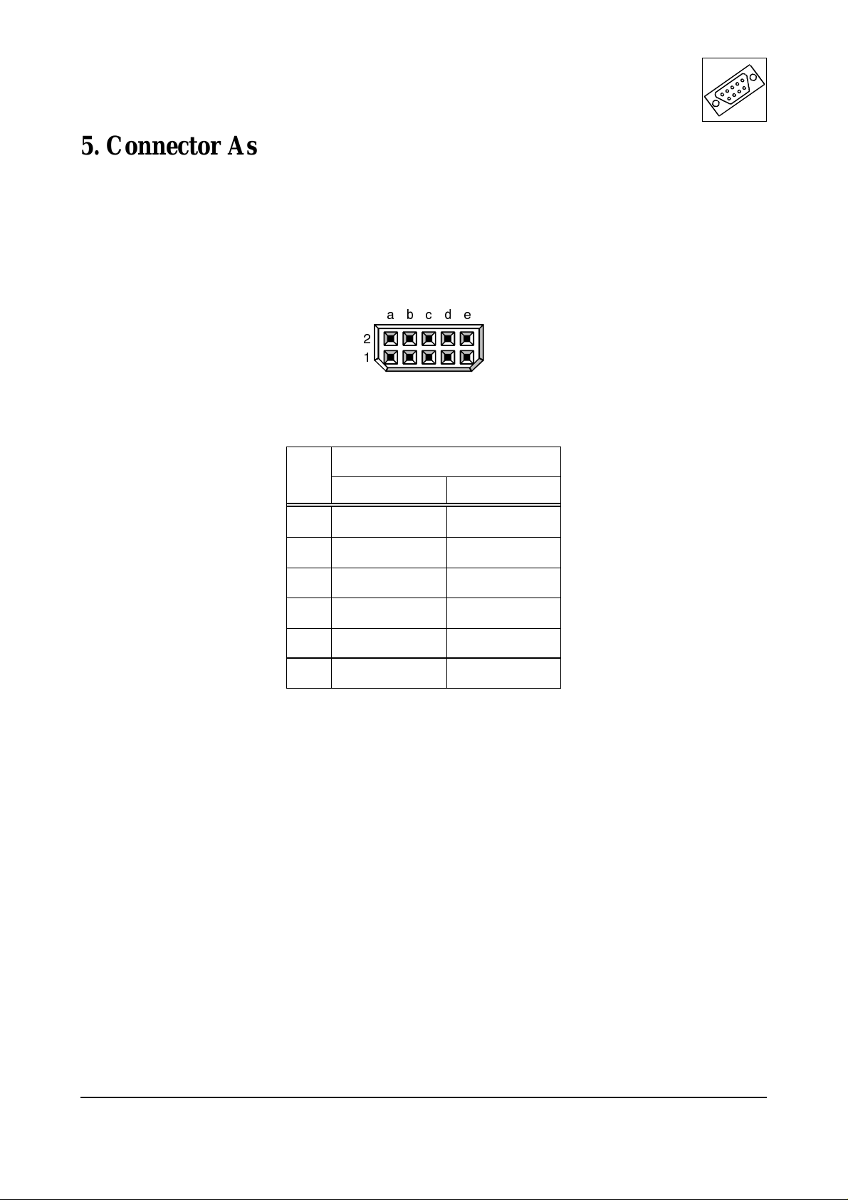
Device connector: har-link® female multipoint connector 10-pin, Harting Nr.: 27211218000
Pin Position:
a b c d e
2
1
Pin Assignment:
Signal
Pin
Row 1 Row 2
a TXS1 RXS1
b RTSS1# CTSS1#
c TXS2 RXS2
d RTSS2# CTSS2#
e GND +5V
z Shield Shield
Signal description:
TXSx, RXSx, RTSSx#,
CTSSx#
... Data and control signals of the serial interfaces 1 and 2 (x = 1, 2).
The signal direction is seen from the VME-PMC-CADDY/2 (i.e.
TXSx = output).
Attention: The signals TXS1, RXS1, TXS2 and RXS2 are also
connected to VMEbus via P0 (see page 29).
GND ... Reference potential of the serial interface
+5V ... Power supply voltage, connected with +5V of the VMEbus,
max. permissible load I
< 100 mA
Load
Shield ... Contacts of the metal shield of the har-link socket. Shield is
connected to the front panel of the VME-PMC-CADDY/2.
VME-PMC-CADDY/2
Hardware-Manual • Doc.-No.: V.1915.21 / Rev. 1.0
Page 23 of 43
Page 24
Connector Assignment
5.2 Adapter Cable “VME-PMC-CPU/Cable”
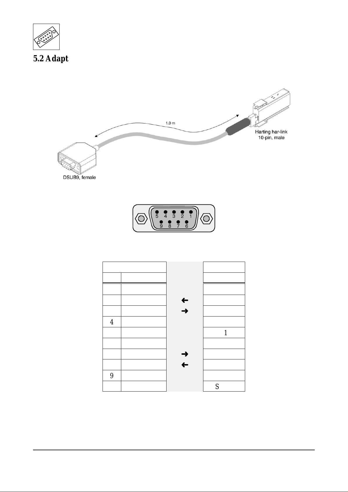
An adapter cable from 10-pin har-link to 9-pin DSUB (order No.: V.1917.25). is available for the
connection of the serial interface 1.
Pin Position DSUB9:
12345
6789
Pin Assignment:
DSUB9
Pin Signal Pin
Signal
direction *
har-link
1 - 2 TXS1
3 RXS1
³
þ
a1
a2
4 - 5 GND e1
6 - 7 CTSS1#
8 RTSS1#
þ
³
b2
b1
9 - -
- Shield Shield
* The signal direction is described as seen from the VME-PMC-CADDY/2.
-... This pin is not connected.
See page 23 for signal description.
Page 24 of 43
Hardware Manual • Doc. No.: V.1915.21 / Rev. 1.0
VME-PMC-CADDY/2
Page 25
Connector Assignment
5.3 Adapter Cable “VME-PMC-CPU/Cable-Y”
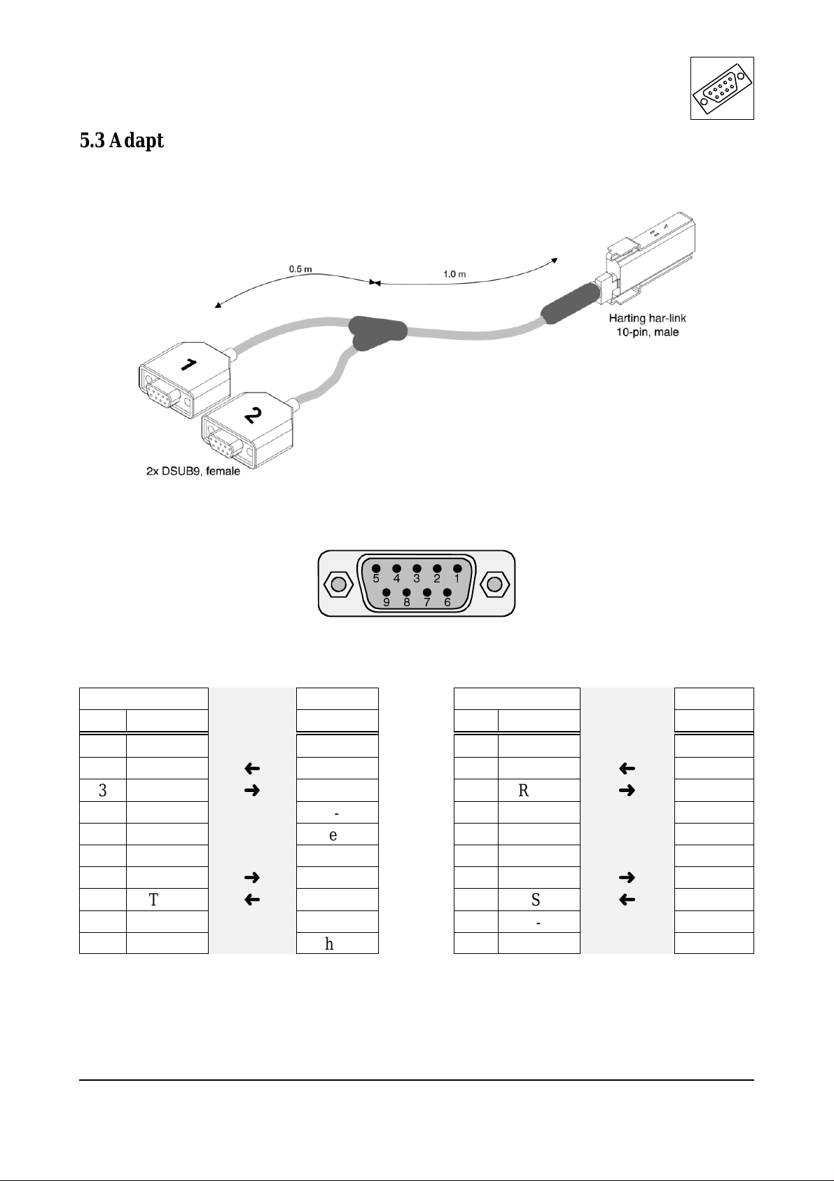
An adapter cable with Y-junction from 10-pin har-link to 2x 9-pin DSUB (order No.: V.1917.26). is
available for the connection of the serial interfaces 1 and 2.
Pin Position in the DSUB9 Socket:
12345
6789
Pin Assignment:
DSUB9 “1”
Pin Signal Pin Pin Signal Pin
Signal
direction *
har-link DSUB9 “2”
Signal
direction *
har-link
1 - - 1 - 2 TXS1
3 RXS1
³
þ
a1 2 TXS2
a2 3 RXS2
³
þ
c1
c2
4 - - 4 - 5 GND e1 5 GND e1
6 - - 6 - 7 CTSS1#
8 RTSS1#
þ
³
b2 7 CTSS2#
b1 8 RTSS2#
þ
³
d2
d1
9 - - 9 - -
- Shield Shield - Shield Shield
* The signal direction is described as seen from the VME-PMC-CADDY/2.
-... This pin is not connected.
See page 23 for signal description.
VME-PMC-CADDY/2
Hardware-Manual • Doc.-No.: V.1915.21 / Rev. 1.0
Page 25 of 43
Page 26
Connector Assignment
5.4 VMEbus P1
Pin Row z Row a Row b Row c Row d Pin
1
2
3
4
5
6
7
8
9
10
11
12
13
14
15
16
17
18
19
20
21
22
23
24
25
26
27
28
29
30
31
32
GND
GND
GND
GND
GND
GND
GND
GND
GND
GND
GND
GND
GND
GND
GND
GND
D00
D01
D02
D02
D04
D05
D06
D07
GND
SYSCLK
GND
DS1*
DS0*
WRITE*
GND
DTACK*
GND
AS*
GND
IACK*
IACKIN*
IACKOUT*
AM4
A07
A06
A05
A04
A03
A02
A01
-12 V
+5 V
BBSY*
BCLR*
ACFAIL*
BG0IN*
BG0OUT*
BG1IN*
BG1OUT*
BG2IN*
BG2OUT*
BG3IN*
BG3OUT*
BR0*
BR1*
BR2*
BR3*
AM0
AM1
AM2
AM3
GND
-
GND
IRQ7*
IRQ6*
IRQ5*
IRQ4*
IRQ3*
IRQ2*
IRQ1*
+5V STBY
+5 V
D08
D09
D10
D11
D12
D13
D14
D15
GND
SYSFAIL*
BERR*
SYSRESET*
LWORD*
AM5
A23
A22
A21
A20
A19
A18
A17
A16
A15
A14
A13
A12
A11
A10
A09
A08
+12 V
+5 V
GND
-
-
-
-
-
GAP*
GA0*
GA1*
+3.3V
GA2*
+3.3V
GA3*
+3.3V
GA4*
+3.3V
+3.3V
+3.3V
+3.3V
+3.3V
+3.3V
+3.3V
GND
-
1
2
3
4
5
6
7
8
9
10
11
12
13
14
15
16
17
18
19
20
21
22
23
24
25
26
27
28
29
30
31
32
160-pin VG-connector according to DIN41612
I
per pin : 1.0 A
max
- ... Signal is not connected on the board
Page 26 of 43
Hardware Manual • Doc. No.: V.1915.21 / Rev. 1.0
VME-PMC-CADDY/2
Page 27
Connector Assignment
5.5 Standard Assignment of I/O-Signals
5.5.1 Standard Assignment VMEbus P2 (According to VITA 35, P4 V2-64ac)
In the standard assignment the I/O signals of the PMC slot 1 (J14) are connected to the rows a+c.
Pin Row z Row a Row b Row c Row d Pin
1
2
3
4
5
6
7
8
9
10
11
12
13
14
15
16
17
18
19
20
21
22
23
24
25
26
27
28
29
30
31
32
GND
GND
GND
GND
GND
GND
GND
GND
GND
GND
GND
GND
GND
GND
GND
GND
I/O102
I/O104
I/O106
I/O108
I/O110
I/O112
I/O114
I/O116
I/O118
I/O120
I/O122
I/O124
I/O126
I/O128
I/O130
I/O132
I/O134
I/O136
I/O138
I/O140
I/O142
I/O144
I/O146
I/O148
I/O150
I/O152
I/O154
I/O156
I/O158
I/O160
I/O162
I/O164
+5 V
GND
BRETRY*
A24
A25
A26
A27
A28
A29
A30
A31
GND
+5 V
D16
D17
D18
D19
D20
D21
D22
D23
GND
D24
D25
D26
D27
D28
D29
D30
D31
GND
+5 V
I/O101
I/O103
I/O105
I/O107
I/O109
I/O111
I/O113
I/O115
I/O117
I/O119
I/O121
I/O123
I/O125
I/O127
I/O129
I/O131
I/O133
I/O135
I/O137
I/O139
I/O141
I/O143
I/O145
I/O147
I/O149
I/O151
I/O153
I/O155
I/O157
I/O159
I/O161
I/O163
-
-
-
-
-
-
-
-
-
-
-
-
-
-
-
-
-
-
-
-
-
-
-
-
-
-
-
-
-
GND
-
1
2
3
4
5
6
7
8
9
10
11
12
13
14
15
16
17
18
19
20
21
22
23
24
25
26
27
28
29
30
31
32
160-pin VG-connector according to DIN41612
I
per Pin : 1.0 A
max
- ...
VME-PMC-CADDY/2
Signal is not connected on the board
Hardware-Manual • Doc.-No.: V.1915.21 / Rev. 1.0
Page 27 of 43
Page 28
Connector Assignment
5.5.2 Standard Assignment of Transfer Module with P2 Row a and c Signals
The table below shows the assignment of a 64-pole transfer module connected to P2 connector. The 64
contacts of the module are connected to the signals of the rows a and c of the connector P2. Thus all
I/O-contacts of the PMC slot 1 (J14) are accessible via the transfer module.
Assignment of a 64-pin transfer module
Assignment of the I/O connector P2
Pin
Pin
Row a Signal Row c
2
4
6
8
10
12
14
16
18
20
22
24
26
28
30
32
34
36
38
40
42
44
46
48
50
52
54
56
58
60
62
64
1
2
3
4
5
6
7
8
9
10
11
12
13
14
15
16
17
18
19
20
21
22
23
24
25
26
27
28
29
30
31
32
I/O102
I/O104
I/O106
I/O108
I/O110
I/O112
I/O114
I/O116
I/O118
I/O120
I/O122
I/O124
I/O126
I/O128
I/O130
I/O132
I/O134
I/O136
I/O138
I/O140
I/O142
I/O144
I/O146
I/O148
I/O150
I/O152
I/O154
I/O156
I/O158
I/O160
I/O162
I/O164
I/O101
I/O103
I/O105
I/O107
I/O109
I/O111
I/O113
I/O115
I/O117
I/O119
I/O121
I/O123
I/O125
I/O127
I/O129
I/O131
I/O133
I/O135
I/O137
I/O139
I/O141
I/O143
I/O145
I/O147
I/O149
I/O151
I/O153
I/O155
I/O157
I/O159
I/O161
I/O163
1
2
3
4
5
6
7
8
9
10
11
12
13
14
15
16
17
18
19
20
21
22
23
24
25
26
27
28
29
30
31
32
1
3
5
7
9
11
13
15
17
19
21
23
25
27
29
31
33
35
37
39
41
43
45
47
49
51
53
55
57
59
61
63
Page 28 of 43
Hardware Manual • Doc. No.: V.1915.21 / Rev. 1.0
VME-PMC-CADDY/2
Page 29
Connector Assignment
5.5.3 Standard Assignment VMEbus P0
Pin Row f Row e Row d Row c Row b Row a
1 GND - - GND - 2 GND - - GND - 3 GND RXS2 TXS2 RXS1 TXS1 GND
4 GND I/O201 I/O202 I/O203 I/O204 I/O205
5 GND I/O206 I/O207 I/O208 I/O209 I/O210
6 GND I/O211 I/O212 I/O213 I/O214 I/O215
7 GND I/O216 I/O217 I/O218 I/O219 I/O220
8 GND I/O221 I/O222 I/O223 I/O224 I/O225
9 GND - - - - 10 GND - - - - 11 GND - - - - 12 GND I/O226 I/O227 I/O228 I/O229 I/O230
13 GND I/O231 I/O232 I/O233 I/O234 I/O235
14 GND I/O236 I/O237 I/O238 I/O239 I/O240
15 GND I/O241 I/O242 I/O243 I/O244 I/O245
16 GND I/O246 I/O247 I/O248 I/O249 I/O250
17 GND I/O251 I/O252 I/O253 I/O254 I/O255
18 GND I/O256 I/O257 I/O258 I/O259 I/O260
19 GND I/O261 I/O262 I/O263 I/O264 do not connect
95-pin I/O connector according to IEC 1076-4-101
Description of the signals of P0:
RXSy, TXSy ... Serial interfaces 1 and 2 (y = 1, 2), physical layer RS-232
(These signals are bridged with the signals of the same name of connector
X1940 in the front panel. Do not use at the same time!)
I/O201 ... I/O264 ... I/O signals of the PMC slot 2 (J24) according to VITA 35, P4 V0-64
do not connect ... Do not connect this pin.
- ... This pin is not connected on the board.
VME-PMC-CADDY/2
Hardware-Manual • Doc.-No.: V.1915.21 / Rev. 1.0
Page 29 of 43
Page 30
Connector Assignment
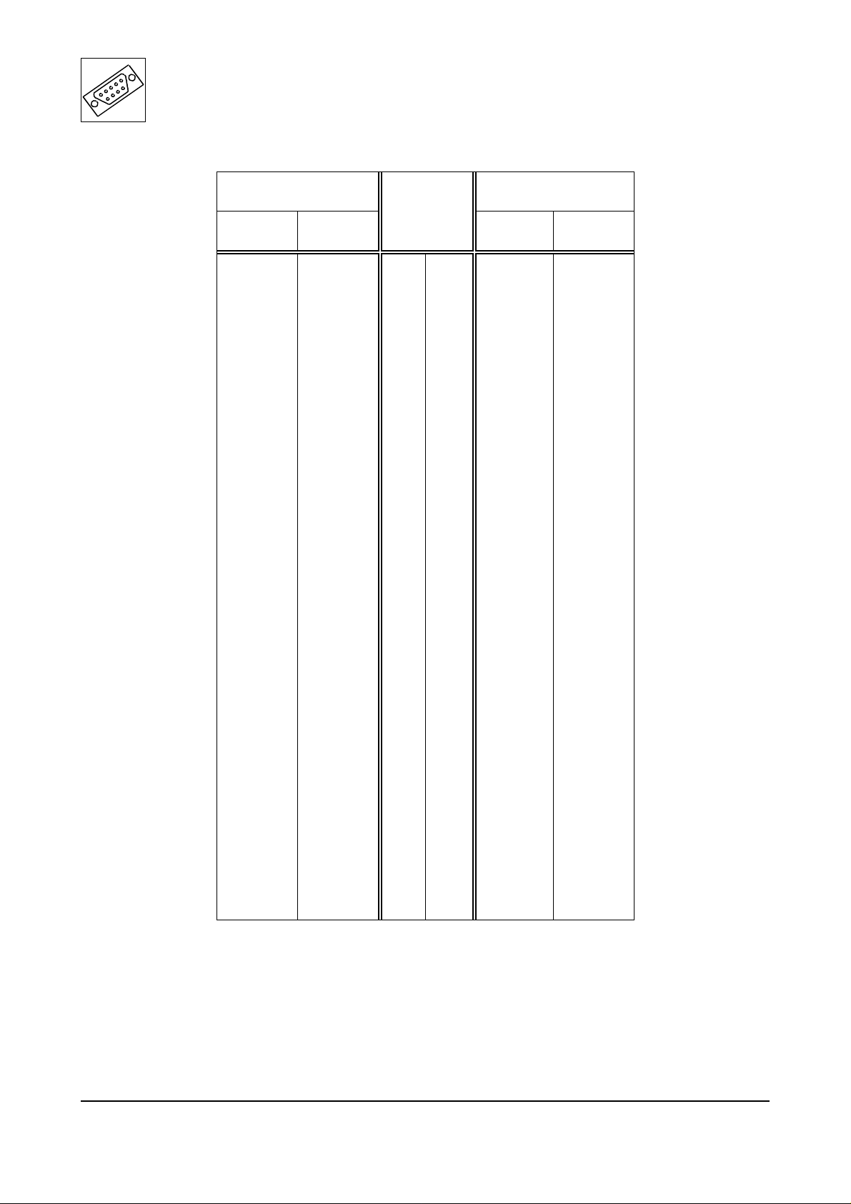
5.5.4 Standard Assignment of the I/O Connector J14 at PMC Slot 1
Signal
Pin No
Signal
of
Name to P2-Pin Name to P2-Pin
I/O101
I/O103
I/O105
I/O107
I/O109
I/O111
I/O113
I/O115
I/O117
I/O119
I/O121
I/O123
I/O125
I/O127
I/O129
I/O131
I/O133
I/O135
I/O137
I/O139
I/O141
I/O143
I/O145
I/O147
I/O149
I/O151
I/O153
I/O155
I/O157
I/O159
I/O161
I/O163
c1
c2
c3
c4
c5
c6
c7
c8
c9
c10
c11
c12
c13
c14
c15
c16
c17
c18
c19
c20
c21
c22
c23
c24
c25
c26
c27
c28
c29
c30
c31
c32
1
3
5
7
9
11
13
15
17
19
21
23
25
27
29
31
33
35
37
39
41
43
45
47
49
51
53
55
57
59
61
63
J14
2
4
6
8
10
12
14
16
18
20
22
24
26
28
30
32
34
36
38
40
42
44
46
48
50
52
54
56
58
60
62
64
I/O102
I/O104
I/O106
I/O108
I/O110
I/O112
I/O114
I/O116
I/O118
I/O120
I/O122
I/O124
I/O126
I/O128
I/O130
I/O132
I/O134
I/O136
I/O138
I/O140
I/O142
I/O144
I/O146
I/O148
I/O150
I/O152
I/O154
I/O156
I/O158
I/O160
I/O162
I/O164
a1
a2
a3
a4
a5
a6
a7
a8
a9
a10
a11
a12
a13
a14
a15
a16
a17
a18
a19
a20
a21
a22
a23
a24
a25
a26
a27
a28
a29
a30
a31
a32
Page 30 of 43
Socket connector 2x32
Hardware Manual • Doc. No.: V.1915.21 / Rev. 1.0
VME-PMC-CADDY/2
Page 31
Connector Assignment
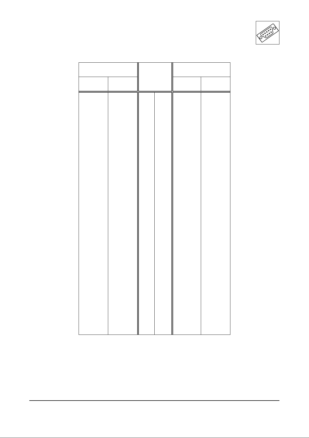
5.5.5 Standard Assignment of the I/O Connector J24 at PMC Slot 2
Signal
Pin No.
Signal
of
Name to P0-Pin Name to P0-Pin
I/O201
I/O203
I/O205
I/O207
I/O209
I/O211
I/O213
I/O215
I/O217
I/O219
I/O221
I/O223
I/O225
I/O227
I/O229
I/O231
I/O233
I/O235
I/O237
I/O239
I/O241
I/O243
I/O245
I/O247
I/O249
I/O251
I/O253
I/O255
I/O257
I/O249
I/O261
I/O263
e4
c4
a4
d5
b5
e6
c6
a6
d7
b7
e8
c8
a8
d12
b12
e13
c13
a13
d14
b14
e15
c15
a15
d16
b16
e17
c17
a17
d18
b18
e19
c19
1
3
5
7
9
11
13
15
17
19
21
23
25
27
29
31
33
35
37
39
41
43
45
47
49
51
53
55
57
59
61
63
J24
2
4
6
8
10
12
14
16
18
20
22
24
26
28
30
32
34
36
38
40
42
44
46
48
50
52
54
56
58
60
62
64
I/O202
I/O204
I/O206
I/O208
I/O210
I/O212
I/O214
I/O216
I/O218
I/O220
I/O222
I/O224
I/O226
I/O228
I/O230
I/O232
I/O234
I/O236
I/O238
I/O240
I/O242
I/O244
I/O246
I/O248
I/O250
I/O252
I/O254
I/O256
I/O258
I/O260
I/O262
I/O264
d4
b4
e5
c5
a5
d6
b6
e7
c7
a7
d8
b8
e12
c12
a12
d13
b13
e14
c14
a14
d15
b15
e16
c16
a16
d17
b17
e18
c18
a18
d19
b19
Socket connector 2x32
VME-PMC-CADDY/2
Hardware-Manual • Doc.-No.: V.1915.21 / Rev. 1.0
Page 31 of 43
Page 32
Connector Assignment
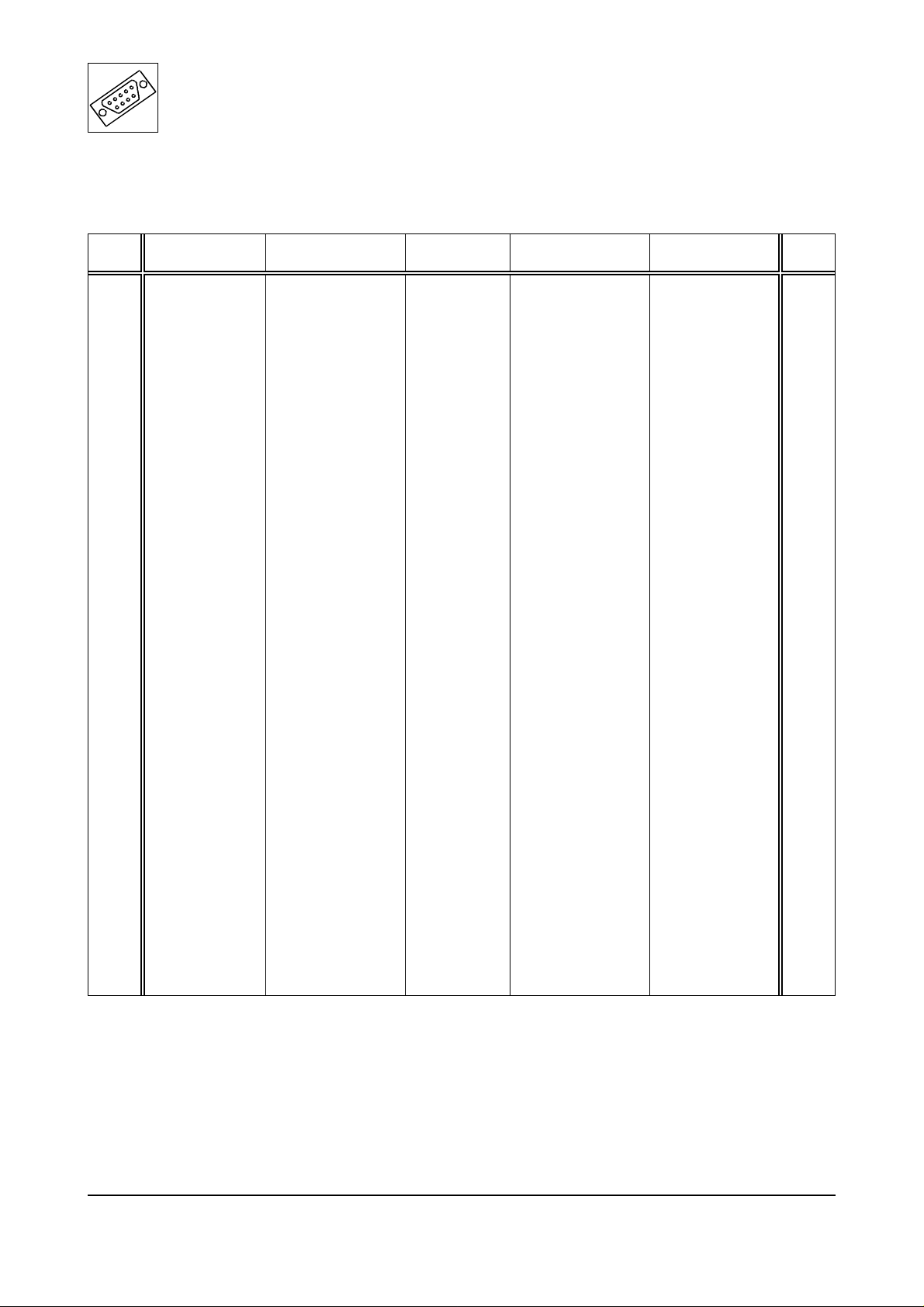
5.6 Assignment of the I/O-Signals using the‘-32P2’ Option
5.6.1 Assignment VMEbus P2 using ‘-32P2’ Option
Pin Row z Row a Row b Row c Row d Pin
1
2
3
4
5
6
7
8
9
10
11
12
13
14
15
16
17
18
19
20
21
22
23
24
25
26
27
28
29
30
31
32
GND
GND
GND
GND
GND
GND
GND
GND
GND
GND
GND
GND
GND
GND
GND
GND
I/O102+I/O234
I/O104+I/O236
I/O106+I/O238
I/O108+I/O240
I/O110+I/O242
I/O112+I/O244
I/O114+I/O246
I/O116+I/O248
I/O118+I/O250
I/O120+I/O252
I/O122+I/O254
I/O124+I/O256
I/O126+I/O258
I/O128+I/O260
I/O130+I/O262
I/O132+I/O264
I/O134
I/O136
I/O138
I/O140
I/O142
I/O144
I/O146
I/O148
I/O150
I/O152
I/O154
I/O156
I/O158
I/O160
I/O162
I/O164
+5 V
GND
BRETRY*
A24
A25
A26
A27
A28
A29
A30
A31
GND
+5 V
D16
D17
D18
D19
D20
D21
D22
D23
GND
D24
D25
D26
D27
D28
D29
D30
D31
GND
+5 V
I/O101+I/O233
I/O103+I/O235
I/O105+I/O237
I/O107+I/O239
I/O109+I/O241
I/O111+I/O243
I/O113+I/O245
I/O115+I/O247
I/O117+I/O249
I/O119+I/O251
I/O121+I/O253
I/O123+I/O255
I/O125+I/O257
I/O127+I/O259
I/O129+I/O261
I/O131+I/O263
I/O133
I/O135
I/O137
I/O139
I/O141
I/O143
I/O145
I/O147
I/O149
I/O151
I/O153
I/O155
I/O157
I/O159
I/O161
I/O163
-
-
-
-
-
-
-
-
-
-
-
-
-
-
-
-
-
-
-
-
-
-
-
-
-
-
-
-
-
GND
-
1
2
3
4
5
6
7
8
9
10
11
12
13
14
15
16
17
18
19
20
21
22
23
24
25
26
27
28
29
30
31
32
160-pin VG-connector according to
I
per pin : 1.0 A
max
- ...
Page 32 of 43
Signal is not connected on the board
Hardware Manual • Doc. No.: V.1915.21 / Rev. 1.0
DIN41612
VME-PMC-CADDY/2
Page 33
Connector Assignment
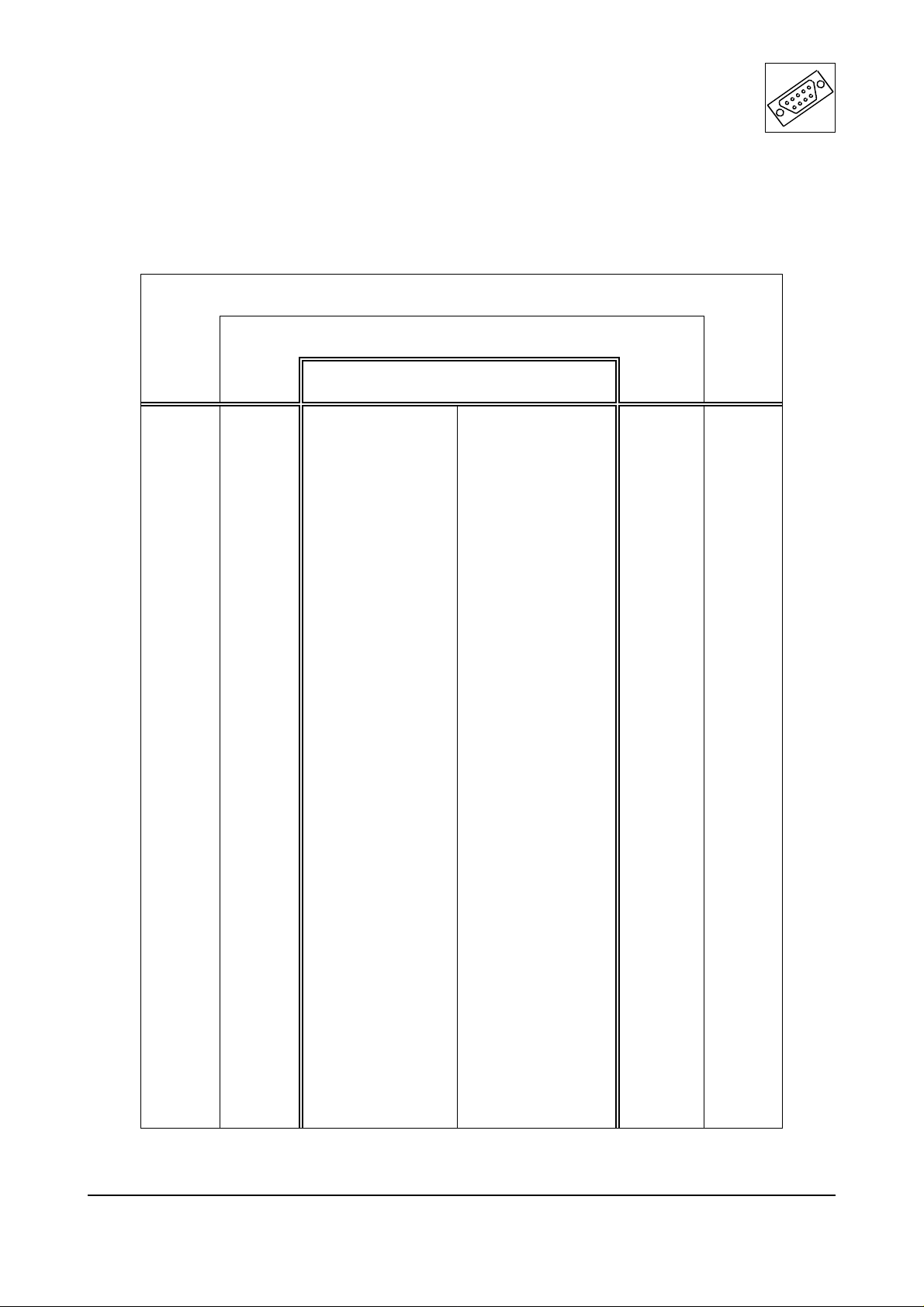
5.6.2 Assignment of a Transfer Module at ‘-32P2’ Option
The following table shows the assignment of a 64-pin transfer module when connected to the P2
connector. The 64 contacts of the module are connected to the signals of the rows a and c of the
connector P2.
Assignment of a 64-pin Transfer Module
Assignment of the I/O Connector P2
Pin
Pin
Row a Signal Row c
2
4
6
8
10
12
14
16
18
20
22
24
26
28
30
32
34
36
38
40
42
44
46
48
50
52
54
56
58
60
62
64
1
2
3
4
5
6
7
8
9
10
11
12
13
14
15
16
17
18
19
20
21
22
23
24
25
26
27
28
29
30
31
32
I/O102+I/O234
I/O104+I/O236
I/O106+I/O238
I/O108+I/O240
I/O110+I/O242
I/O112+I/O244
I/O114+I/O246
I/O116+I/O248
I/O118+I/O250
I/O120+I/O252
I/O122+I/O254
I/O124+I/O256
I/O126+I/O258
I/O128+I/O260
I/O130+I/O262
I/O132+I/O264
I/O134
I/O136
I/O138
I/O140
I/O142
I/O144
I/O146
I/O148
I/O150
I/O152
I/O154
I/O156
I/O158
I/O160
I/O162
I/O164
I/O101+I/O233
I/O103+I/O235
I/O105+I/O237
I/O107+I/O239
I/O109+I/O241
I/O111+I/O243
I/O113+I/O245
I/O115+I/O247
I/O117+I/O249
I/O119+I/O251
I/O121+I/O253
I/O123+I/O255
I/O125+I/O257
I/O127+I/O259
I/O129+I/O261
I/O131+I/O263
I/O133
I/O135
I/O137
I/O139
I/O141
I/O143
I/O145
I/O147
I/O149
I/O151
I/O153
I/O155
I/O157
I/O159
I/O161
I/O163
1
2
3
4
5
6
7
8
9
10
11
12
13
14
15
16
17
18
19
20
21
22
23
24
25
26
27
28
29
30
31
32
1
3
5
7
9
11
13
15
17
19
21
23
25
27
29
31
33
35
37
39
41
43
45
47
49
51
53
55
57
59
61
63
VME-PMC-CADDY/2
Hardware-Manual • Doc.-No.: V.1915.21 / Rev. 1.0
Page 33 of 43
Page 34
Connector Assignment
5.6.3 Assignment VMEbus P0 at ‘-32P2’ Option
Pin Row f Row e Row d Row c Row b Row a
1 GND - - GND - 2 GND - - GND - 3 GND RXS2 TXS2 RXS1 TXS1 GND
4 GND I/O201 I/O202 I/O203 I/O204 I/O205
5 GND I/O206 I/O207 I/O208 I/O209 I/O210
6 GND I/O211 I/O212 I/O213 I/O214 I/O215
7 GND I/O216 I/O217 I/O218 I/O219 I/O220
8 GND I/O221 I/O222 I/O223 I/O224 I/O225
9 GND - - - - 10 GND - - - - 11 GND - - - - 12 GND I/O226 I/O227 I/O228 I/O229 I/O230
13 GND I/O231 I/O232 I/O101+I/O233 I/O102+I/O234 I/O103+I/O235
14 GND I/O104+I/O236 I/O105+I/O237 I/O106+I/O238 I/O107+I/O239 I/O108+I/O240
15 GND I/O109+I/O241 I/O110+I/O242 I/O111+I/O243 I/O112+I/O244 I/O113+I/O245
16 GND I/O114+I/O246 I/O115+I/O247 I/O116+I/O248 I/O117+I/O249 I/O118+I/O250
17 GND I/O119+I/O251 I/O120+I/O252 I/O121+I/O253 I/O122+I/O254 I/O123+I/O255
18 GND I/O124+I/O256 I/O125+I/O257 I/O126+I/O258 I/O127+I/O259 I/O128+I/O260
19 GND I/O129+I/O261 I/O130+I/O262 I/O131+I/O263 I/O132+I/O264 do not connect
95-pin I/O connector according to IEC 1076-4-101
Description of the signals of P0:
RXSy, TXSy ... Serial interfaces 1 and 2 (y = 1, 2), physical layer RS-232
(These signals are bridged with the signals of the same name of connector X1940 in the
front panel. Do not use at the same time!)
I/O201 ... I/O232 ... I/O-signals of PMC-Slot 2 (J24)
I/O101+I/O233 ...
I/O132+I/O264
do not connect ... Do not connect this pin.
- ... This pins is not connected on the board.
Page 34 of 43
... bridged I/O-signals of the PMC-slots 1 (J14) and 2 (J24)
Hardware Manual • Doc. No.: V.1915.21 / Rev. 1.0
VME-PMC-CADDY/2
Page 35
5.6.4 Assignment of the PMC Connector J14 at ‘-32P2’ Option
Connector Assignment
I/O101
I/O103
I/O105
I/O107
I/O109
I/O111
I/O113
I/O115
I/O117
I/O119
I/O121
I/O123
I/O125
I/O127
I/O129
I/O131
I/O133
I/O135
I/O137
I/O139
I/O141
I/O143
I/O145
I/O147
I/O149
I/O151
I/O153
I/O155
I/O157
I/O159
I/O161
I/O163
Name
+
I/O233
+
I/O235
+
I/O237
+
I/O239
+
I/O241
+
I/O243
+
I/O245
+
I/O247
+
I/O249
+
I/O251
+
I/O253
+
I/O255
+
I/O257
+
I/O249
+
I/O261
+
I/O263
Signal
P2Pin
c1
c2
c3
c4
c5
c6
c7
c8
c9
c10
c11
c12
c13
c14
c15
c16
c17
c18
c19
c20
c21
c22
c23
c24
c25
c26
c27
c28
c29
c30
c31
c32
Signal
P0-
J24-
Pin
J14-Pin
Pin
+
c13
+
a13
+
d14
+
b14
+
e15
+
c15
+
a15
+
d16
+
b16
+
e17
+
c17
+
a17
+
d18
+
b18
+
e19
+
c19
33
35
37
39
41
43
45
47
49
51
53
55
57
59
61
63
1
3
5
7
9
11
13
15
17
19
21
23
25
27
29
31
33
35
37
39
41
43
45
47
49
51
53
55
57
59
61
63
10
12
14
16
18
20
22
24
26
28
30
32
34
36
38
40
42
44
46
48
50
52
54
56
58
60
62
64
J24-
Pin
P2Pin
2
4
6
8
34
36
38
40
42
44
46
48
50
52
54
56
58
60
62
64
a1
a2
a3
a4
a5
a6
a7
a8
a9
a10
a11
a12
a13
a14
a15
a16
a17
a18
a19
a20
a21
a22
a23
a24
a25
a26
a27
a28
a29
a30
a31
a32
P0Pin
+
b13
+
e14
+
c14
+
a14
+
d15
+
b15
+
e16
+
c16
+
a16
+
d17
+
b17
+
e18
+
c18
+
a18
+
d19
+
b19
I/O102
I/O104
I/O106
I/O108
I/O110
I/O112
I/O114
I/O116
I/O118
I/O120
I/O122
I/O124
I/O126
I/O128
I/O130
I/O132
Name
+
I/O234
+
I/O236
+
I/O238
+
I/O240
+
I/O242
+
I/O244
+
I/O246
+
I/O248
+
I/O250
+
I/O252
+
I/O254
+
I/O256
+
I/O258
+
I/O260
+
I/O262
+
I/O264
I/O134
I/O136
I/O138
I/O140
I/O142
I/O144
I/O146
I/O148
I/O150
I/O152
I/O154
I/O156
I/O158
I/O160
I/O162
I/O164
Socket connector 2x32
Reading the Table - Examples:
Pin 9 of the PMC-connector J14 is connected with pin 41 of the PMC connector J24. Furthermore pin 9 is connected to the
pins c5 and z27 of the VMEbus-connector P2. In the schematic diagram the signal names I/O109 and I/O241 are used for
this net.
VME-PMC-CADDY/2
Hardware-Manual • Doc.-No.: V.1915.21 / Rev. 1.0
Page 35 of 43
Page 36
Connector Assignment
5.6.5 Assignment of the PMC Connector J24 at ‘-32P2’ Option
I/O201
I/O203
I/O205
I/O207
I/O209
I/O211
I/O213
I/O215
I/O217
I/O219
I/O221
I/O223
I/O225
I/O227
I/O229
I/O231
I/O233
I/O235
I/O237
I/O239
I/O241
I/O243
I/O245
I/O247
I/O249
I/O251
I/O253
I/O255
I/O257
I/O249
I/O261
I/O263
Name
+
I/O101
+
I/O103
+
I/O105
+
I/O107
+
I/O109
+
I/O111
+
I/O113
+
I/O115
+
I/O117
+
I/O119
+
I/O121
+
I/O123
+
I/O125
+
I/O127
+
I/O129
+
I/O131
Signal
P2Pin
c1
c2
c3
c4
c5
c6
c7
c8
c9
c10
c11
c12
c13
c14
c15
c16
Signal
P0-
J14-
Pin
J24-Pin
Pin
e4
c4
a4
d5
b5
e6
c6
a6
d7
b7
e8
c8
a8
d12
b12
e13
+
c13
+
a13
+
d14
+
b14
+
e15
+
c15
+
a15
+
d16
+
b16
+
e17
+
c17
+
a17
+
d18
+
b18
+
e19
+
c19
1
3
5
7
9
11
13
15
17
19
21
23
25
27
29
31
1
3
5
7
9
11
13
15
17
19
21
23
25
27
29
31
33
35
37
39
41
43
45
47
49
51
53
55
57
59
61
63
2
4
6
8
10
12
14
16
18
20
22
24
26
28
30
32
34
36
38
40
42
44
46
48
50
52
54
56
58
60
62
64
J14-
Pin
2
4
6
8
10
12
14
16
18
20
22
24
26
28
30
32
P2Pin
a1
a2
a3
a4
a5
a6
a7
a8
a9
a10
a11
a12
a13
a14
a15
a16
P0Pin
d4
b4
e5
c5
a5
d6
b6
e7
c7
a7
d8
b8
e12
c12
a12
d13
+
b13
+
e14
+
c14
+
a14
+
d15
+
b15
+
e16
+
c16
+
a16
+
d17
+
b17
+
e18
+
c18
+
a18
+
d19
+
b19
I/O202
I/O204
I/O206
I/O208
I/O210
I/O212
I/O214
I/O216
I/O218
I/O220
I/O222
I/O224
I/O226
I/O228
I/O230
I/O232
I/O234
I/O236
I/O238
I/O240
I/O242
I/O244
I/O246
I/O248
I/O250
I/O252
I/O254
I/O256
I/O258
I/O260
I/O262
I/O264
Name
+
I/O102
+
I/O104
+
I/O106
+
I/O108
+
I/O110
+
I/O112
+
I/O114
+
I/O116
+
I/O118
+
I/O120
+
I/O122
+
I/O124
+
I/O126
+
I/O128
+
I/O130
+
I/O132
Socket connector 2x32
Page 36 of 43
Hardware Manual • Doc. No.: V.1915.21 / Rev. 1.0
VME-PMC-CADDY/2
Page 37
Connector Assignment
5.7 Special Assembly: J24-I/O-Signals to d+z of P2 (acc. VITA 35, P4 V2-46dz)
5.7.1 Assignment of P2 at Special Assembly with RC800, RC801, ...RC811
In this special assembly the I/O signals of the PMC slot 2 (J24) are not only connected to P0 but in
parallel to this also to the rows d+z of P2.
For this assembly there is currently no ordering option specified. Please contact our sales team if you
are interested in this special option: [email protected]
Pin Row z Row a Row b Row c Row d Pin
1
2
3
4
5
6
7
8
9
10
11
12
13
14
15
16
17
18
19
20
21
22
23
24
25
26
27
28
29
30
31
32
I/O202
GND
I/O205
GND
I/O208
GND
I/O211
GND
I/O214
GND
I/O217
GND
I/O220
GND
I/O223
GND
I/O226
GND
I/O229
GND
I/O232
GND
I/O235
GND
I/O238
GND
I/O241
GND
I/O244
GND
I/O246
GND
I/O102
I/O104
I/O106
I/O108
I/O110
I/O112
I/O114
I/O116
I/O118
I/O120
I/O122
I/O124
I/O126
I/O128
I/O130
I/O132
I/O134
I/O136
I/O138
I/O140
I/O142
I/O144
I/O146
I/O148
I/O150
I/O152
I/O154
I/O156
I/O158
I/O160
I/O162
I/O164
+5 V
GND
BRETRY*
A24
A25
A26
A27
A28
A29
A30
A31
GND
+5 V
D16
D17
D18
D19
D20
D21
D22
D23
GND
D24
D25
D26
D27
D28
D29
D30
D31
GND
+5 V
I/O101
I/O103
I/O105
I/O107
I/O109
I/O111
I/O113
I/O115
I/O117
I/O119
I/O121
I/O123
I/O125
I/O127
I/O129
I/O131
I/O133
I/O135
I/O137
I/O139
I/O141
I/O143
I/O145
I/O147
I/O149
I/O151
I/O153
I/O155
I/O157
I/O159
I/O161
I/O163
I/O201
I/O203
I/O204
I/O206
I/O207
I/O209
I/O210
I/O212
I/O213
I/O215
I/O216
I/O218
I/O219
I/O221
I/O222
I/O224
I/O225
I/O227
I/O228
I/O230
I/O231
I/O233
I/O234
I/O236
I/O237
I/O239
I/O240
I/O242
I/O243
I/O245
GND
-
1
2
3
4
5
6
7
8
9
10
11
12
13
14
15
16
17
18
19
20
21
22
23
24
25
26
27
28
29
30
31
32
160-pin VG-connector according to
VME-PMC-CADDY/2
DIN41612, I
Hardware-Manual • Doc.-No.: V.1915.21 / Rev. 1.0
per Pin : 1.0 A, - ...
max
Signal is not connected on the board
Page 37 of 43
Page 38
Connector Assignment
5.7.2 Assignment I/O Connector J24 at Assembly with RC800, RC801, ...RC811
Signal
Signal
J24-Pin
Name an P2-Pin Name an P2-Pin
I/O201
I/O203
I/O205
I/O207
I/O209
I/O211
I/O213
I/O215
I/O217
I/O219
I/O221
I/O223
I/O225
I/O227
I/O229
I/O231
I/O233
I/O235
I/O237
I/O239
I/O241
I/O243
I/O245
I/O247
I/O249
I/O251
I/O253
I/O255
I/O257
I/O249
I/O261
I/O263
d1
d2
z3
d5
d6
z7
d9
d10
z11
d13
d14
z15
d17
d18
z19
d21
d22
z23
d25
d26
z27
d29
d30
-
-
-
-
-
-
-
-
-
1
3
5
7
9
11
13
15
17
19
21
23
25
27
29
31
33
35
37
39
41
43
45
47
49
51
53
55
57
59
61
63
2
4
6
8
10
12
14
16
18
20
22
24
26
28
30
32
34
36
38
40
42
44
46
48
50
52
54
56
58
60
62
64
I/O202
I/O204
I/O206
I/O208
I/O210
I/O212
I/O214
I/O216
I/O218
I/O220
I/O222
I/O224
I/O226
I/O228
I/O230
I/O232
I/O234
I/O236
I/O238
I/O240
I/O242
I/O244
I/O246
I/O248
I/O250
I/O252
I/O254
I/O256
I/O258
I/O260
I/O262
I/O264
z9
z1
d3
d4
z5
d7
d8
d11
d12
z13
d15
d16
z17
d19
d20
z21
d23
d24
z25
d27
d28
z29
z31
-
-
-
-
-
-
-
-
-
Page 38 of 43
Socket connector 2x32
Hardware Manual • Doc. No.: V.1915.21 / Rev. 1.0
VME-PMC-CADDY/2
Page 39
Connector Assignment
5.8 XMC Socket J15 (Option)
For this assembly there is currently no ordering option specified. Please contact our sales team if you
are interested in this special option: [email protected]
Row
Pin
a b c d e f
1 PER_0_P PER_0_N 3,3V PER_1_P PER_1_N VPWR
2 GND GND PCI-TRST# GND GND PORST#
3 PER_2_P PER_2_N 3,3V PER_3_P PWER_3_N VPWR
4 GND GND PCI-TCK GND GND XMC_RSTO#
5 - - 3,3V - - VPWR
6 GND GND PCI-TMS GND GND +12V
7 - - 3,3V - - VPWR
8 GND GND PCI-TD2 GND GND -12V
9 - - - - - VPWR
10 GND GND PCI-TDO GND GND GND
11 PET_0_P PET_0_N XMC_BIST# PET_1_P PET_1_N VPWR
12 GND GND GND GND GND XMC_PRSNT#
13 PET_2_P PET_2_N 3,3VAUX PET_3_P PET_3_N VPWR
14 GND GND 3,3V GND GND IIC2_SDA
15 - - - - - VPWR
16 GND GND GND GND GND IIC2_SCL
17 - - - - - 18 GND GND - GND GND 19 REFCLK_1_P REF_CLK_1_N - - - -
VME-PMC-CADDY/2
Hardware-Manual • Doc.-No.: V.1915.21 / Rev. 1.0
Page 39 of 43
Page 40

Connector Assignment
Description of the signals of J15:
PER_x_P,
PER_x_N
PET_x_P,
PET_x_N
PCI-TRST# ...
PORST# ... Card Reset
PCI-TCK,
PCI-TD2,
PCI-TMS
XMC_RSTO# ... This signal is triggered by the XMC card.
XMC_BIST# ... This pin is not connected on the board.
XMC_PRSNT# ... PMC module detection signal
IIC2_SDA,
IIC2_SCL
REFCLK_1_P,
REFCLK_1_N
... Differential PCI Express receiver signals (x = 0, 1, 2, 3) of the four lanes.
... Differential PCI Express transmitter signals (x = 0, 1, 2, 3) of the four lanes.
... PCI-JTAG interface
... I²C data- and clock signal (IPMI support)
... 100 MHz PCI Express reference clock
GND ... Reference potential
VPWR ... Power supply voltage +5V ( selectable via solder bridges, VPWR can be
alternatively connected to the 12V supply voltage of the VMEbus; please contact
our sales team for this)
3,3V ... Power supply voltage +3,3V
3,3VAUX ... 3,3V AUX generated of +5V STBY supplied by VMEbus
+12V/-12V ... Power supply voltage +12V and -12V
- ... These pins are not connected on the board.
Page 40 of 43
Hardware Manual • Doc. No.: V.1915.21 / Rev. 1.0
VME-PMC-CADDY/2
Page 41

6. References
[1] Tsi148™PCI/X-to-VME Bus Bridge User Manual,
Tundra Semiconductor Corporation,
referenced document version: 80A3020_MA001_10, April 2008
document source: http://www.tundra.com/products/vme-bridges/tsi148/resources
References
VME-PMC-CADDY/2
Hardware-Manual • Doc.-No.: V.1915.21 / Rev. 1.0
Page 41 of 43
Page 42
Order Information
7. Order Information
Type Properties Order No.
VME-PMC-CADDY/2
VMEbus base board for two single PMC modules,
standard temperature range: 0 /C...+50 /C,
P2-pin assignment acc. to to VITA 35 (P4V264ac, P4V0-64), (no interconnection between
PMC modules), no XMC, 3.3V supply for PMC
fed from VMEbus
V.1915.02
VME-PMC-CADDY/2-T
VME-PMC-CADDY/2-32P2
VME-PMC-CADDY/2-T-32P2
VME-PMC-CADDY/2-CC
VME-PMC-CADDY/2-CC-32P2
Accessories
VME-PMC-CPU/Cable
VME-PMC-CPU/Cable-Y
as V.1915.02, but for extended temperature
range: - 40 /C ...+85 /C
VMEbus base board for two single PMC modules,
P2-pin assignment acc. to IEEE Std 1386-2001,
Table 8 (interconnection between 16 pins of the
PMC-modules), no XMC, 3.3V supply for PMC
fed from VMEbus
as V.1915.11, but for extended temperature
range: - 40 /C...+85 /C
as V.1915.02, but conduction cooled,
extended temperature range: - 40 /C...+85 /C
as V.1915.11, but conduction cooled,
extended temperature range: - 40 /C...+85 /C
Adapter cable for serial interface 1 (RS232) from
har-link10 to DSUB9 socket, length: 1.0 m
For details see page 24
Adapter cable for serial interface 1 and 2 (RS232),
Y-junction from har-link10 to 2x DSUB9 socket,
length: 1.5m
For details see page 25
V.1915.03
V.1915.11
V.1915.13
V.1916.02
V.1916.11
V.1917.25
V.1917.26
Software
VME-PMC-CADDY/2-VxWorks-LIB VxWorks Library V.1915.58
For detailed information about the driver availability for your operating system, please contact our sales
team.
Table 11: Order information
Page 42 of 43
Hardware Manual • Doc. No.: V.1915.21 / Rev. 1.0
VME-PMC-CADDY/2
Page 43
Order Information
PDF Manuals
Manuals are available in English and usually in German as well. For availability of English manuals
see the following table.
Please download the manuals as PDF documents from our esd website www.esd.eu for free.
Manuals Order No.
VME-PMC-CADDY/2-MD
VME-PMC-CADDY/2-ME
Hardware manual in German V.1915.20
Hardware manual in English V.1915.21
Table 12: Available manuals
Printed Manuals
If you need a printout of the manual additionally, please contact our sales team: [email protected] for a
quotation. Printed manuals may be ordered for a fee.
VME-PMC-CADDY/2
Hardware-Manual • Doc.-No.: V.1915.21 / Rev. 1.0
Page 43 of 43
 Loading...