

ESD VME - ASIO16 User Manual

VMEVME -- ASIO16ASIO16
1616 serialserial InterfacesInterfaces
VME-ASIO16 Rev. 1.7

NOTE
The information in this document has been carefully checked and is
believed to be entirely reliable. esd makes no warranty of any kind
with regard to the material in this document, and assumes no responsibility for any errors that may appear in this document. esd reserves the right to make changes without notice to this, or any of its
products, to improve reliability, performance or design.
esd assumes no responsibility for the use of any circuitry other
than circuitry which is part of a product of esd gmbh.
esd does not convey to the purchaser of the product described herein
any license under the patent rights of esd gmbh nor the rights of
others.
esd electronic system design gmbh
Vahrenwalder Str. 207
D-30165 Hannover
Germany
Phone: +49-511-37298-0
FAX: +49-511-37298-68
This document shall not be duplicated, nor its contents used
for any purpose, unless express permission has been granted.
Copyright by esd
VME-ASIO16 Rev. 1.7
Manual file: ...\MANUALS\VME\asio1617.en6 14.11.97
Described ASIO16 1.1
PCB version
Described ASIO4.0
firmware version
Changes in the chapters
The changes in the user’s manual listed below affect changes in the
firmware, as well as changes in the description of the facts only.
Chapter Alternations versus rev. 1.6
1.4.3.1 Correction of P2’s pin assignment in fig. 1.4.2
Further technical data are subject to change without notice.
VME-ASIO16 Rev. 1.7

VME-ASIO16 Rev. 1.7

User’s Manual VME-ASIO16
Content Page
1. Hardware .......................... 5
1.1 Block Diagram .................... 5
1.2 Technical Data .................... 6
1.2.1 Overview ................... 6
1.2.2 Real-time Software .............. 6
1.2.3 Summary of the Technical Data ......... 7
1.2.4 Order Information ............... 9
1.3 Address Selection on the VME-ASIO16 ......... 11
1.4 Configuration Jumpers ................ 13
1.4.1 Default Setting ................ 14
1.4.2 VMEbus Interface Jumpers ........... 15
1.4.2.1 The Address Modifier (AM) and DS1 at BR3 15
1.4.2.2 Base Address Decoding via Jumpers BR1
andBR2 ................ 19
1.4.2.3 Interrupt Levels ............ 20
1.4.3 Jumperfields of the Serial Interfaces ..... 21
1.4.3.1 Feeding of the Power Supply ...... 21
1.4.3.2 Selection between RS-232 and TTY
Interfaces ............... 23
1.4.3.3 Control Signals of the Serial Interfaces 26
1.5 Serial Interfaces .................. 29
1.5.1 Circuitry of the Serial Interfaces ...... 29
1.5.2 The RS-232 Interface ............. 30
1.5.3 The TTY Interface ............... 30
1.6 Interrupt Processing ................. 31
2. RTOS-UH Software Support .................. 33
2.1 Survey Channel Structure ............... 33
2.2 Parameter Channel .................. 34
2.2.1 Structure of the Parameter Channel Ix.PARA
(Px.) ..................... 34
2.2.2 Description of the Parameters in Particular . . 35
VME-ASIO16 Rev. 1.7 1

Content Page
3. Appendix .......................... 39
3.1 Connector Pin Assignments .............. 39
3.1.1 VMEbus P1 ................... 39
3.1.2 I/O Connector P2
(at Internal Supply of the TTY Interface) . . . 40
3.1.3 I/O Connector P2
(at External Supply of the TTY Interface) . . . 41
3.1.4 I/O-Connector P2 (if ASIO RS422 Add On is used) 42
3.2 ASIO16 Adaptor (VME-ASIO-ADAPT) ........... 43
3.2.1 General .................... 43
3.2.2 View of the ASIO16 Adaptor .......... 44
3.2.3 Jumpers of the ASIO16 Adaptor ......... 45
3.2.3.1 Power Supply Selection via BR21 to BR25 45
3.2.3.2 Fixing of the Connector Pin Assignment
via BR1 to BR16 ............ 47
3.2.4 Covering of the 14 pole Connector Plug on the
ASIO16 P2 Adapter ............... 49
3.2.5 Connector Pin Assignment RS-232 via Flat Cable
to DSUB-15 or to DSUB-25 Females ....... 50
3.2.6 Connector Pin Assignment TTY via Flat Cable to
DSUB-9, DSUB-15 or to DSUB-25 Females ..... 51
3.2.7 Connector Pin Assignment RS422 via Flat Cable
to DSUB-15 or to DSUB-25 Females ....... 52
3.3 Add-On ’ASIO-422’ .................. 53
3.3.1 General .................... 53
3.3.2 View of the ASIO422-Add-Ons .......... 53
3.3.3 Jumpers of the ASIO422 Add-On ......... 54
3.3.3.1 Selection of the Power Supply via the
Jumpers J1 to J3 ............ 54
3.4 Front Panel ..................... 55
3.5 Circuit Diagrams ................... 57
3.6 Data Sheets ..................... 59
VME-ASIO16 Rev. 1.72

User’s Manual VME-ASIO16
Contents of Figures Page
Fig. 1.1.1: Block Diagram of the VME-ASIO16 .......... 5
Fig. 1.4.1: Position of the Jumpers on the ASIO16 ....... 13
Fig. 1.4.2: Wiring of the External TTY Interfaces Power Supply 22
Fig. 1.4.3: Block Diagram of the Interfaces .......... 23
Fig. 1.5.1: Circuitry of the Serial Interfaces
(Example: Channel 1) ............... 29
Fig. 3.2.1: View of the ASIO16 Adapter with Designation of the
Jumpers ...................... 44
Fig. 3.3.1: Top Overlay Placement of the RS-422 Add-Ons with
Marking of the Jumpers .............. 53
Contents of Tables
Table 1.2.1: General Data of the VME-ASIO16 .......... 8
Table 1.2.2: Order Information ................ 9
Table 1.3.1: Address Model of the VME-ASIO16 ......... 11
Table 1.4.1: Default Jumper Setting .............. 14
Table 1.4.2: AM Configuration of the VME-ASIO16 ........ 15
Table 1.4.3: Recommended Access Modes for Standard Accesses
(A24) ...................... 17
Table 1.4.4: Recommended Access Modes for Standard Accesses
(A16) ...................... 18
Table 1.4.5: Channel Assignment to the Jumpers BR33 to BR40 . . 26
Table 1.4.6: Functions of the DUART68681 Ports ........ 26
Table 2.1.1: Data Station Designation ............ 33
VME-ASIO16 Rev. 1.7 3

VME-ASIO16 Rev. 1.74
Overview
1. Hardware
1.1 Block Diagram
Fig. 1.1.1: Block Diagram of the VME-ASIO16
VME-ASIO16 Rev. 1.7 5

Overview
1.2 Technical Data
1.2.1 Overview
The VME-ASIO16 is an input/output board for asynchronous serial data
transfer via 16 channels. Each channel can be operated as a RS-232
interface or as a 20 mA current loop. The operation mode can be
selected for each channel separately by jumpers. All signal and
supply lines are fed via the P2 connector.
The current loop interfaces are provided with electrical isolation
via optocouplers. For operation as current loop interfaces ±12 V
power can be supplied either externally via P2 or internally via the
VMEbus. The current sources for transmission and reception signals
are located on the board (active current source). At operation as
RS-232C interface the data lines and handshakes are available even
in the base version.
An interrupt logic with priority control generates a common interrupt on the VMEbus for each two channels. The interrupt level is
selectable from 1 to 7 by jumpers. An interrupt is also generated at
a line break of the 20 mA current loop.
Alternatively (Add-on-Board) the board can be equipped with up to 12
channels of RS-422 (optoisolated) and 4 channels of RS-232.
The channel handling is performed by up to 8 DUART 68681, depending
on the equipment of the board.
1.2.2 Real-time Software
Driver packages for the VME-ASIO16 are available for operating
systems such as VxWorks, OS-9 and others.
VME-ASIO16 Rev. 1.76
Overview
1.2.3 Summary of the Technical Data
VMEbus specification
VMEbus interface IEEE P1014/D1.2 (Rev. C)
data transfer SADO24 - slave with A24/D16 access
options SD16 - slave with A16/D16 access
address modifier complete evaluation of AM0 to AM5,
(AM) additionally with don’t care mode
base address selectable via jumpers over the whole
address range of 16 Mbytes.
The board covers 256 bytes.
serial interfaces
controller three to eight DUART68681 for each two
channels
standard up to 16 serial asynchronous
interfaces interfaces RS-232C or TTY
selectable via jumpers
programmable Baud rate : 75 baud - 38.4 kbaud,
interface (max. 9600 baud at TTY)
parameters characters: 5, 6, 7, 8
parity : NONE, ODD, EVEN, FORCE
PARITY ODD, FORCE PARITY
EVEN
stop bits: 0.563 to 2.000 programmable
in steps of 1/16
options ADD-ON for 12 x RS-422 and 4 x RS-232
VME-ASIO16 Rev. 1.7 7
Overview
General Data
temperature range 0...70° C
humidity max. 90%, non-condensing
connector types P1 - DIN 41612-C96
P2 - DIN 41612-C64
board size 160 mm x 233 mm
VME dimensions 6 U height/ 1 slot width
front panel with pc board ejectors
weight 460g at insertion of 16 channels of
RS-232/TTY
(without add-on and adapters)
power consumption VMEbus P1: 5V ±5% / max. 1A
VMEbus P2: +12V ±5% / 200mA *1)
-12V ±5% / 200mA *1)
*1) At external supply of the TTY interfaces
Table 1.2.1: General Data of the VME-ASIO16
VME-ASIO16 Rev. 1.78
Overview
1.2.4 Order Information
Name Description Order no.
VME-ASIO16-6 6 channels RS-232 or V.1401.06
20 mA current loop (active) *)
VME-ASIO16-8 8 channels RS-232 or V.1401.08
20 mA current loop (active) *)
VME-ASIO16-12 12 channels RS-232 or V.1401.12
20 mA current loop (active) *)
VME-ASIO16-16 16 channels RS-232 or V.1401.16
20 mA current loop (active) *)
VME-ASIO-422 add-on for VME-ASIO16, for V.1401.00
max. 12x RS-422 + 4x RS-232
VME-ASIO16-ADAPT adapter module with connector V.1401.02
plugs for connection of
DSUB females to P2
VME-ASIO16-ISO Special version of the V.1401.30
VME-ASIO16 ’TTY passive’
VME-ASIO16-C C driver for OS-9 as P.1401.50
source code
VME-ASIO16-MD user’s manual in German M.1401.20
VME-ASIO16-ME user’s manual in English M.1401.21
*) A user’s manual (available in German and in English) is contained in
the extent of delivery.
Table 1.2.2: Order Information
VME-ASIO16 Rev. 1.7 9

VME-ASIO16 Rev. 1.710
Address Covering
1.3 Address Selection on the VME-ASIO16
The setting of the base board address ensues via jumpers of the
jumperfields BR1 and BR2. The base address can be selected over the
whole address range of 16 Mbytes in steps of 256 bytes.
Additionally it is possible to use the VME addressing mode ’SHORT I/O’. At this addressing the address lines A16 to A23 are ignored
and the base address of the VME-ASIO16 is placed into the ’SHORT
I/O’ address range (64 kbytes) of the VMEbus system.
The peripheral components DUART 68681 are provided with an 8 bits
wide data bus and with 4 address lines (A1 to A4). The addresses A5
to A7 select the desired DUART on the VME-ASIO16.
address DUART component
(HEX) 68681
xxxx00-1F 1 J26
xxxx20-3F 2 J25
xxxx40-5F 3 J24
xxxx60-7F 4 J23
xxxx80-9F 5 J22
xxxxA0-BF 6 J21
xxxxC0-DF 7 J20
xxxxE0-FF 8 J19
xxxx.....base address of the ASIO16
Table 1.3.1: Address Model of the VME-ASIO16
For reduced versions of the VME-ASIO16 with less than 16 channels
only a part of the DUARTs will be inserted: starting at the end with
DUART no. 8, e.g. when the board is equipped with 4 channels, the
DUARTs 8 and 7 will be inserted, for 10 channels the DUARTs 8, 7, 6,
5 and 4 will be inserted.
The register model and the meaning of the single bits can be obtained from the data sheet of the DUART 68681 in the appendix.
VME-ASIO16 Rev. 1.7 11

VME-ASIO16 Rev. 1.712
Jumpers Configuration
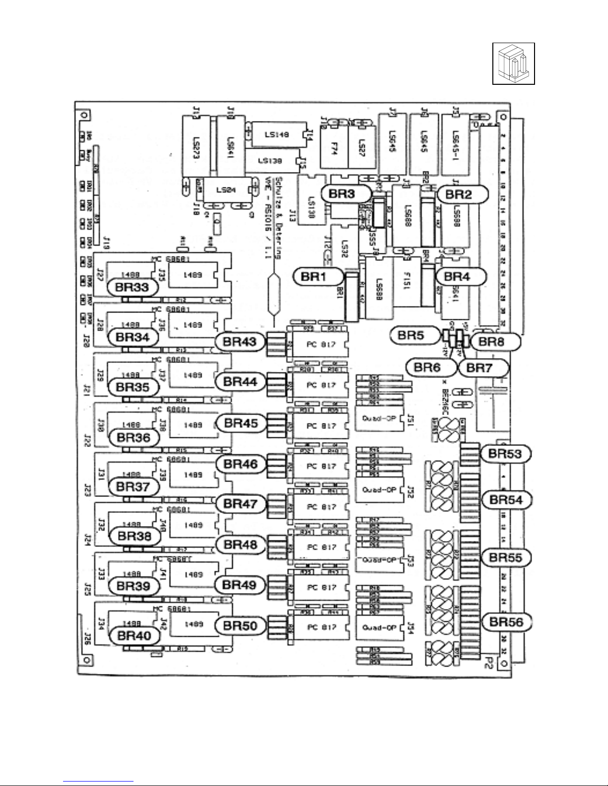
1.4 Configuration Jumpers
Fig. 1.4.1: Position of the Jumpers on the ASIO16
VME-ASIO16 Rev. 1.7 13
Jumpers Configuration
1.4.1 Default Setting
The factory-set (see following table) configuration of the boards is
indicated.
The jumpers location can be obtained from the insertion diagram
(Fig.1.4.1). In the following the jumpers are displayed from the
view of the user, when the board is located in front of him with the
VMEbus connectors to the right (and components on top).
An inserted jumper corresponds to the ’0’(low) level of a signal.
Default jumper setting BR1 to BR50 :
jumper function setting
BR1 addresses A8...A15 base board address
BR2 addresses A16...A23 ASIO16: $800000
BR3 address modifier AM AM2=don’t care, i.e.
access in the supervisory
or user mode (A24)
BR4 VMEbus interrupt interrupt level IRQ4
level inserted
BR5-BR8 selection of the inserted, i.e. the TTY
power supply of interfaces are supplied
the TTY interface via the VMEbus
BR33...BR40 handshake mode ’DTR handshake’
BR43...BR50 DTR, TXD - to all channels to RS-232
RS-232 or TTY operation
BR53...BR56 CTS, RXD - to all channels to RS-232
RS-232 or TTY operation
Table 1.4.1: Default Jumper Setting
VME-ASIO16 Rev. 1.714
Jumpers Configuration
1.4.2 VMEbus Interface Jumpers
1.4.2.1 The Address Modifier (AM) and DS1 at BR3
The address modifier setting ensues at jumperfield BR3. The address
modifiers AM0 to AM5 are completely evaluated. Factory-set is ’Standard Supervisory and Nonprivileged Data Access’ (A24 mode):
12
DS1 o o
AM0 o o
AM1 o o
BR3
AM2 o o
AM4 o o
AM2 don’t care o o
11 12
The ’AM’ configurations permissible for the VME-ASIO16 are:
CODE AM_5 AM_4 AM_3 AM_2 AM_1 AM_0 function
standard
$3E111110supervisory
program access
standard
$3D111101supervisory
data access
standard
$3A111010nonprivileged
program access
standard
$39111001nonprivileged
data access
short
$2D101101supervisory
I/O access
short
$29101001nonprivileged
I/O access
0 = (LOW) jumper inserted, 1 = (HIGH) jumper not inserted
Table 1.4.2: AM Configuration of the VME-ASIO16
VME-ASIO16 Rev. 1.7 15
 Loading...