

Page 1

TF-486
Mainboard
Page 2

Page 3

COPYRIGHT
©
This document is a copyright of the original manufacturer, 1999. The original
manufacturer reserves the right to make improvements to the product(s) described in
this manual at any time without notice. This manual may not, in whole or in part, be
photocopied, reproduced, transcribed, translated, or transmitted in whatever form
without the written consent of the manufacturer, except for copies retained by the
purchaser for backup purposes. All rights are reserved.
TRADEMARKS
The following are trademarks or registered trademarks of their respective companies:
IBM, Intel, AMD, Cyrix, Award, AMI, Microsoft, Windows, Windows NT, Novell, SCO,
PC/104, PICMG, ALI, UMC, SMC, Winbond. Products mentioned in this manual are
mentioned for identification purposes only. All names of products or services appearing
in this manual are the trademarks or registered trademarks of their respective
organizations and companies.
Copyright 1999
Ver. No. 0.0
LEI-UM-TF486-000
Date : 07.08.1999
Page 4

Page 5

TABLE OF CONTENTS
CHAPTER 1 INTRODUCTION 1
1.1 SPECIFICATIONS 2
CHAPTER 2 JUMPER SETTINGS AND CONNECTORS 3
2.1 BOARD OUTLINE OF TF-486 3
2.2 CPU INSTALLING AND UPGRADING 4
2.3 JUMPER SETTING OVERVIEW 5
2.4 JUMPER LOCATION FOR TF-486 6
2.5 JUMPER SETTINGS SUMMARY FOR TF-486 7
2.6 JUMPER SETTINGS FOR TF-486 8
2.7 I/O CONNECTORS LOCATION FOR TF-486 14
2.8 I/O CONNECTORS SUMMARY FOR TF-486 15
2.9 SETTING STATUS INDICATORS AND CONTROL 16
CONNECTORS
2.10 I/O CONNECTORS DESCRIPTION 17
CHAPTER 3 AWARD BIOS SETUP 23
3.1 RUNNING AWARD BIOS 23
3.2 CMOS SETUP UTILITY 24
3.3 STANDARD CMOS SETUP 25
3.4 BIOS FEATURES SETUP 30
3.5 CHIPSET FEATURES SETUP 33
3.6 POWER MANAGEMENT SETUP 35
3.7 PNP/PCI CONFIGURATION 37
3.8 LOAD BIOS DEFAULTS 39
3.9 LOAD SETUP DEFAULTS 39
3.10 INTEGRATED PERIPHERALS 39
3.11 SUPERVISOR / USER PASSWORD 41
3.12 IDE HDD AUTO DETECTION 41
3.13 HDD LOW LEVEL FORMAT 41
3.14 SAVE & EXIT SETUP 42
3.15 EXIT WITHOUT SAVING 43
APPENDIX A HOW TO USE WATCH-DOG TIMER 44
TERMS AND CONDITIONS
RMA SERVICE REQUEST FORM
Page 6

Page 7

TF-486 / 1
CHAPTER 1.
INTRODUCTION
The TF-486 is i
documentation, certification and maintenance.
ESA's revision controlled motherboards reduce your long term costs for system testing,
environments where extensive testing or certification of the system is required.
computer telephony, industrial control, medical instrumentation and other application
control guidelines to provide a long and stable product life cycle. This makes it ideal for
One of the most important qualities of the TF-486 is that it is produced under strict revision
makes it an ideal alternative to expensive passive backplane system architectures.
motherboard. Its compact size, high reliability and large number of expansion slots
ISA cards or one can be PCI that is shared, on an industry standard Baby AT format
class of processors. It supports up to eight expansion cards, all of which can be full length
deal for a broad range of industrial applications utilizing the popular 486
Page 8

INTRODUCTION
TF-486 / 2
1.1 S
PECIFICATIONS
o Processor : PGA socket for Intel® 80486 series, AMD® 486 series
SGS 486 series,and AMD® & Cyrix® 5x86 series
o Chipset : ALi M1487 / M1489
o Bus Clock : 20MHz, 25MHz, 33MHz, 40MHz and 50M Hz
o System Memory : Two 72-pin SIMM sockets up to 64MB EDO/FPM
DRAM
o L2 Cache Memory : 0K cache, supports up to 512KB
o BIOS : 128KB Award License BIOS
o Flash Memory Disk : Reserved one socket for Disk-On-Chip from M-Systems
support up to 144 MB Flash memory Disk-on-Chip
o IDE Drive Interface : Two Fast PCI bus IDE ports that support up to four IDE
devices
o Floppy Drive Interface : One FDD port that supports up to two floppy devices
o Serial Port : Two 16550 compatible FIFO RS-232 serial ports (Box
Header on board) with ESD clamping
o Parallel Port : One multi-mode parallel port (ECP/SPP/EPP) (Box
Header on board) with ESD clamping
o RTC Battery : Dallas RTC battery or compatible
o Mouse Connector : On-board 8-pin PS/2 Mouse header
o Keyboard Connector : On-board 8-pin Keyboard header
o Expansion Slot : Eight ISA and one PCI expansion slots
o Watchdog Timer : 10 level time-out intervals
(0.5/1/2/4/8/16/32/64/128/256 sec)
o IR Interface : Support one IrDA header
o Operating Temperature : 0°C~55°C (32°F~132°F)
o Humidity : 10¢H~90¢H RH
o Dimensions : 257 mm X 222 mm
Page 9
TF-486 / 3
CHAPTER 2.
JUMPER SETTINGS AND CONNECTORS
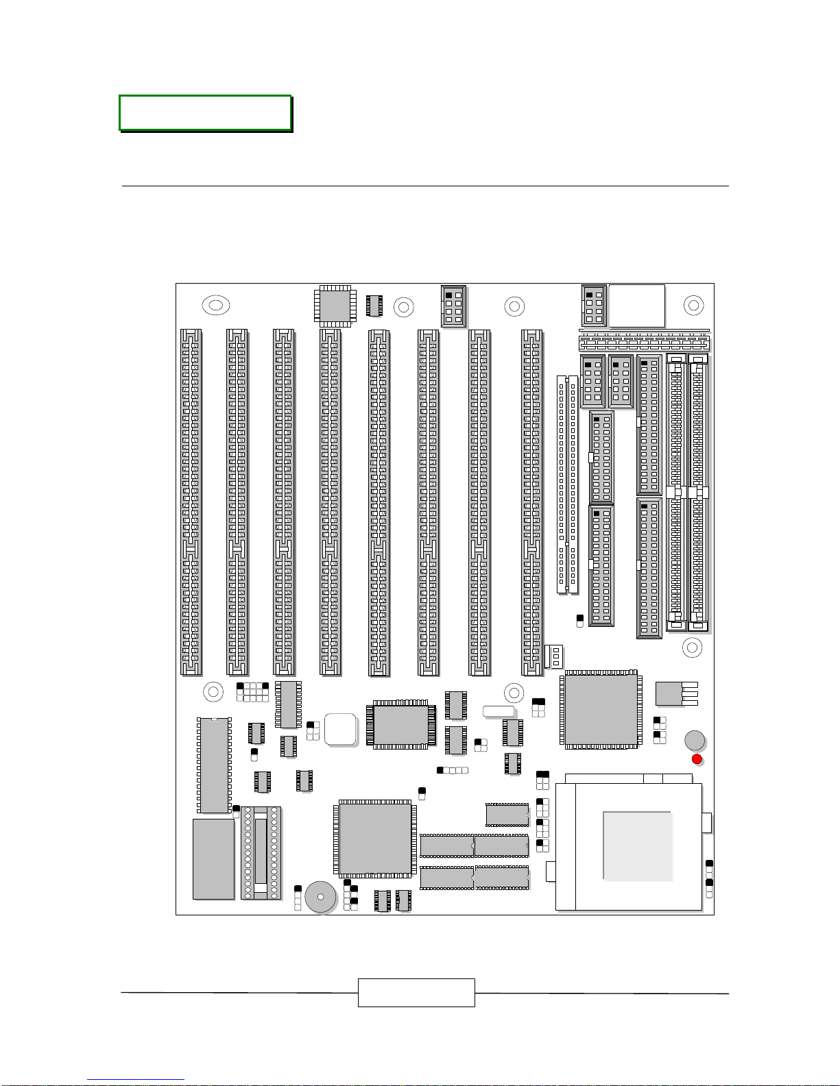
The Figure below shows the jumpers and connectors location on the TF-486
2.1 BOARD OUTLINE OF TF-486
JP4
TF-486
1
3
1
3
FAN1
ISA8
COM1
J1
1
ISA7
ISA6
ISA5
ISA4
ISA3
ISA2
ISA1
SIM1
SIM2
PIDE1
PCI1
PIDE2
RTC
BATTERY
¹
1
4
5
J4
J5
J2
J3
1
JP13
1
5
JP6
JP5
1
1
3 3
JP12
1
2
3
4
JP2
1
2
3
4
JP1
1
3
2
4
JP3
1 2
5
6
JP16
41
123
JP15
10
JP14
2
9
H
L
3
1
11
COM2
PRT1
FDC1
SMI1
1
KB1
PMS1
PS1
ISB1
ISB2
ISB3
ISB4
ISB5
ISB6
ISB7
ISB8
PKB1
JP8
JP7
1
1
3
3
2
6
2
4
1 2
5
6
JP9
JP10
JP11
1
1
5
3
J6
S2
Page 10
JUMPER SETTINGS AND CONNECTORS
TF-486 / 4
2.2 CPU INSTALLING AND UPGRADING
To upgrade to a higher power CPU, simply remove the old CPU and install the new one;
be sure to set the jumpers for the new CPU type and speed.
WARNING!
Disconnect the power cord from your system when you intend to work on it or
you plan to open the chassis of your IPC. Do not make connections when the
power is turned on, the sensitive electronic components could be damaged
by the sudden rush of power. Please only allow experienced electronics
technicians to do this job.
STATIC ELECTRICITY
PRECAUTION!
Caution! Computer components are very sensitive to damage from static
electric discharge. Always ground yourself to remove static charge build-up
before touching the boards in the computer. Use a grounding wrist strap at
all times. Place all electronic components on the anti-static pad for static-
dissipation or in a static-shielded bag when they are not in the chassis.
F
Page 11
JUMPER SETTINGS AND CONNECTORS
TF-486 / 5
2.3 JUMPER SETTING OVERVIEW
In order to select the operation modes of your system, configure and set the jumpers on
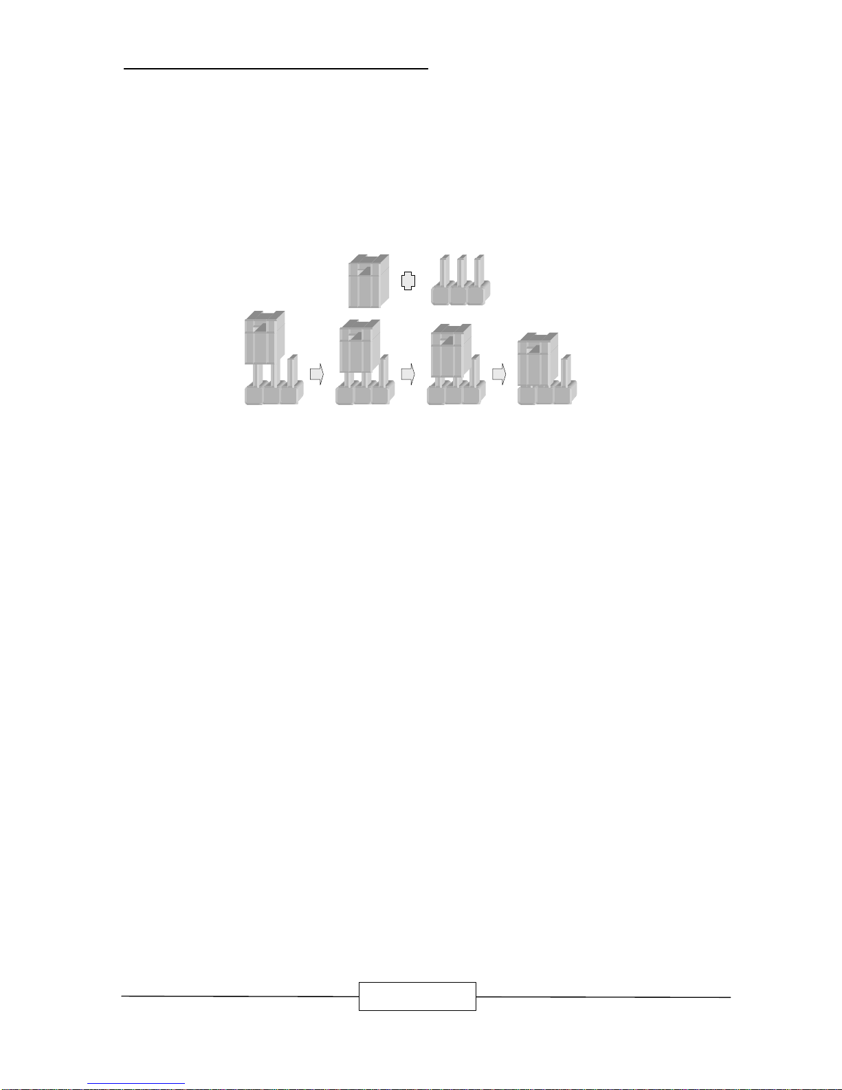
the your MB to match the need of your application. To set a jumper, a plastic cap
containing metal contacts is placed over the jumper pins as designated by the required
configuration as listed in this section. A jumper is said to be “ on ” or “ 1-2 ” when the
black cap has been placed on two of its pins, as show in the figure below:
A pair of needle-nose pliers is recommended when working with jumpers. If you have
any doubts about the best hardware configuration for your application, contact your local
sales representative before you make any changes. In general, you simply need a
standard cable or jumper to make most connections.
Page 12
JUMPER SETTINGS AND CONNECTORS
TF-486 / 6
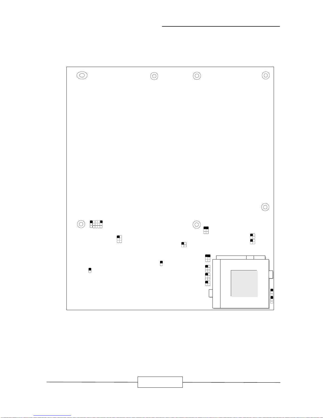
2.4 JUMPER LOCATION BOARD LAYOUT FOR TF-486
JP4
TF-486
1
3
1
3
JP6
JP5
1
1
3 3
JP12
1
2
3
4
JP2
1
2
3
4
JP1
1
3
2
4
JP3
1 2
5
6
JP16
41
123
JP15
10
JP14
2
9
H
L
3
1
11
SMI1
1
JP8
JP7
1
1
3
3
2
6
2
4
1 2
5 6
JP9
JP10
JP11
1
1
5
3
S2
Page 13
JUMPER SETTINGS AND CONNECTORS
TF-486 / 7
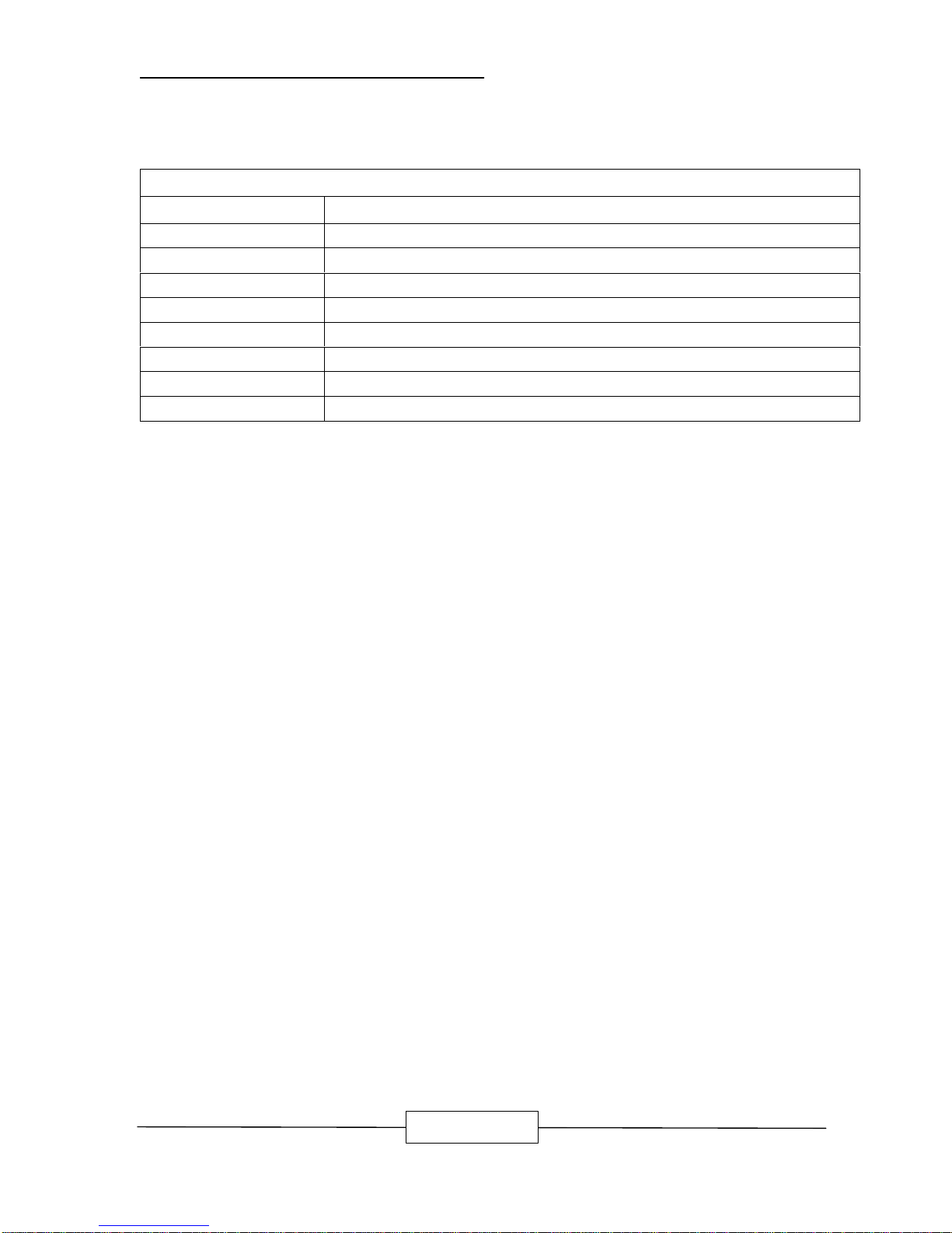
2.5 JUMPER SETTINGS SUMMARY FOR TF-486
JUMPERS
LOCATION FUNCTION
JP1 ~ JP2 Select CPU Voltage
JP3,JP4,JP9 ~ JP11 Select CPU Type
JP5, JP6, JP12 Select CPU Clock
JP7, JP8 Select L2 Cache Size
JP14, JP15 Select Watch-Dog Timer
JP16 Select M-System Address
S2 Clear CMOS Jumper
SMI1 External SMI Function Switch
Page 14
JUMPER SETTINGS AND CONNECTORS
TF-486 / 8
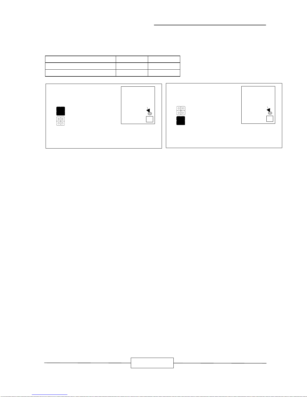
2.6 JUMPER SETTINGS FOR TF-486
l JP1, JP2 : Select CPU Voltage
CPU Voltage JP1 JP2
3.3V (Default) 1-2, 3-4 OFF
5V OFF 1-2, 3-4
CPU Voltage: 3.3V (Default)
JP1
1
2
3
4
JP2
1
2
3
4
JP1
JP2
JP1
1
2
3
4
JP2
1
2
3
4
CPU Voltage: 5V
JP1
JP2
Page 15
JUMPER SETTINGS AND CONNECTORS
TF-486 / 9
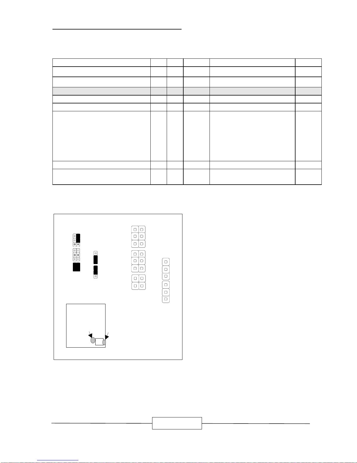
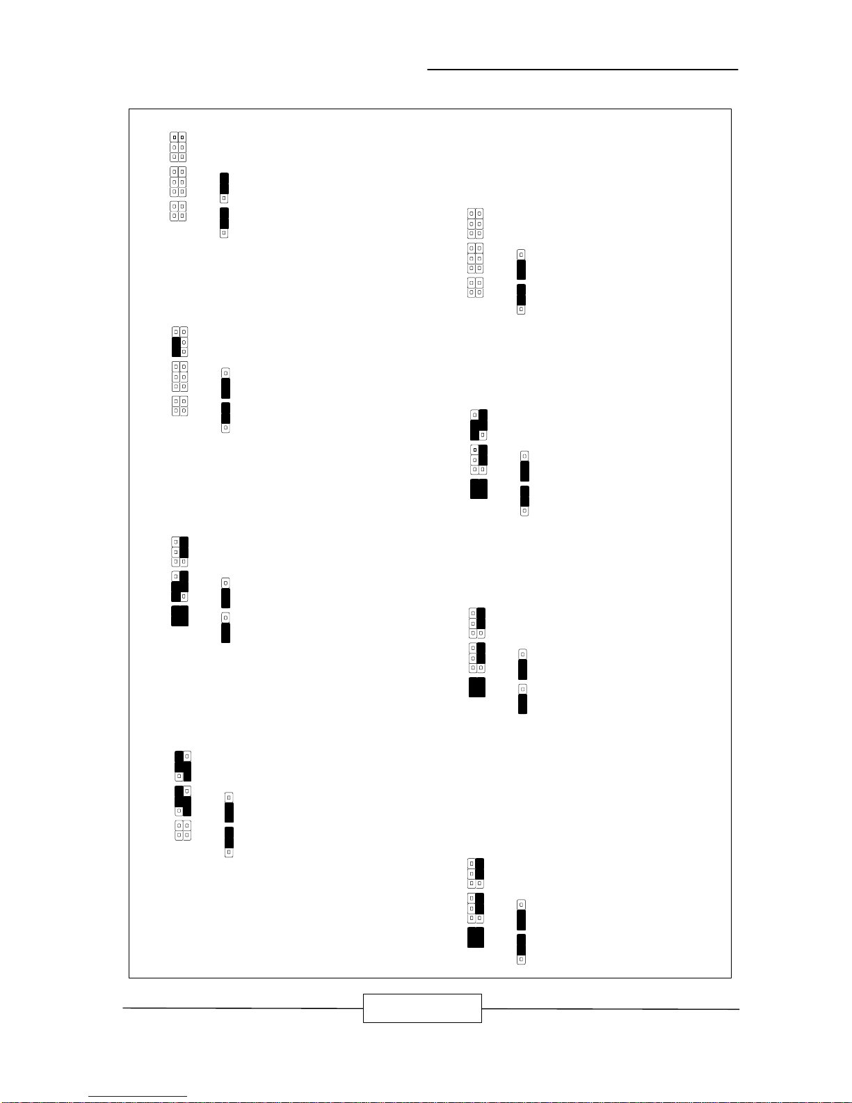
l JP3, JP4, JP9 ~ JP11 : Select CPU Type
CPU Type JP3 JP4 JP9 JP10 JP11
I486SX
1-2 1-2 OFF OFF OFF
I486DX/DX2/ODP;AmDX4-V8T
2-3 1-2 OFF OFF OFF
I486DX4/SL-ENHANCE 2-3 1-2 2-4 OFF 1-2, 3-4
Am486DX2-V8T 2-3 1-2 3-5 OFF OFF
Am486DE2-66V8T 2-3 1-2 2-4, 3-5 2-4 1-2, 3-4
Write Back Enhance CPU
AMD+Am486DX2/DX4-SV8B
AMD+Am5x86-P75
2-3 2-3 2-4
2-4, 3-5: AmDX2-SV8B;
AmD-X5-133/160
2-4: AmDX4-SV8B;
AmD-X5-150;
Intel W/B Enhance CPU
1-2, 3-4
Cyrix Cx486 (DX/DX2/DX4)-GP 2-3 1-2 1-3, 4-6 1-3, 4-6 L1 W/B OFF
Cyrix Cx486DX/DX2/DX4
Cx5x86
2-3 1-2 2-4 2-4 L1-W/B 1-2, 3-4
Note: AMD+ = Enhance SV8B (Internal W/B Cache)
CX486 = TI, ST or SGS, IBM 486; (ST or SGS DX4= Intel DX4)
I486DX4/SL-ENHANCE (Default)
JP4
5
6
JP10
JP3
2
1
152
6
JP9
152
63412
JP10
JP11
131
3
JP10
JP3
JP4
JP9
JP10
JP11
JP3
JP4
JP9
JP11
1
5
1
3
2
6
2
4
1
1
3
3
Page 16
JUMPER SETTINGS AND CONNECTORS
TF-486 / 10
I486SX
152
6
JP9
1526341
2
JP10
JP11
131
3
JP10
JP3
JP4
I486DX/DX2/ODP;AmDX4-V8T
152
6
JP9
152
63412
JP10
JP11
131
3
JP10
JP3
JP4
Am486DX2-V8T
152
6
JP9
1526341
2
JP10
JP11
1
313
JP10
JP3
JP4
Am486DE2-66V8T
152
6
JP9
15263
412
JP10
JP11
131
3
JP10
JP3
JP4
AmDX2-SV8B;
AmD-X5-133/160
152
6
JP9
1526341
2
JP10
JP11
131
3
JP10
JP3
JP4
AmDX4-SV8B;
AmD-X5-150;
INTEL W/B Enhance CPU
152
6
JP9
15263
4
1
2
JP10
JP11
131
3
JP10
JP3
JP4
Cyrix Cx486 (DX/DX2/DX4)-GP
152
6
JP9
1526341
2
JP10
JP11
1
3
1
3
JP10
JP3
JP4
Cyrix Cx486DX/DX2/DX4;
Cx586
152
6
JP9
152
63412
JP10
JP11
131
3
JP10
JP3
JP4
Page 17
JUMPER SETTINGS AND CONNECTORS
TF-486 / 11
JP6
JP12
3
3
1
1
4
2
1
3
JP5
JP12
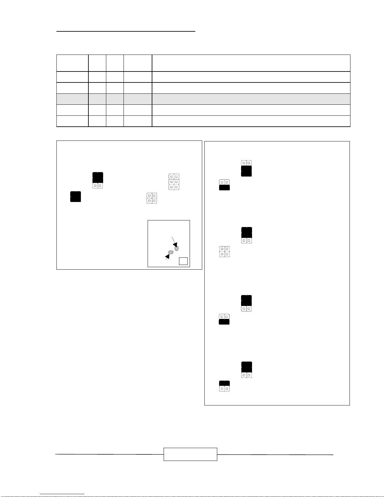
JP5, JP6, JP12 : Select CPU Clock
CPU Bus
Clock
JP5 JP6 JP12 CPU Core Clock
20M Hz 2-3 2-3 3-4
25M Hz 1-2 1-2 OFF
SX-25, SX2-50, DX2-50
33M Hz 1-2 1-2 3-4, 1-2
SX/DX-33, DX2-66, DE2-66,DX4-100,5X86-100,X5-133
40M Hz 1-2 1-2 3-4
DX-40, DX2-80, DX4-120, X5-160
50M Hz 1-2 1-2 1-2
DX-50, X5-150
3
3
1
1
4
2
1
3
JP5
JP6
33M Hz (Default)
SX/DX-33,DX2-66,DE2-66,DX4-100,5X86-100,X5-133
JP5
JP6
JP12
20M Hz
33
1
1
4
2
1
3
JP5JP6
JP12
25M Hz
SX-25,SX2-50, DX2-50
33
1
1
4
2
1
3
JP5JP6
JP12
40M Hz
DX-40,DX2-80,DX4-120,X5-160
33
1
1
4
2
1
3
JP5JP6
JP12
50M Hz
DX-50,X5-150
33
1
1
4
2
1
3
JP5JP6
JP12
Page 18
JUMPER SETTINGS AND CONNECTORS
TF-486 / 12
3
3
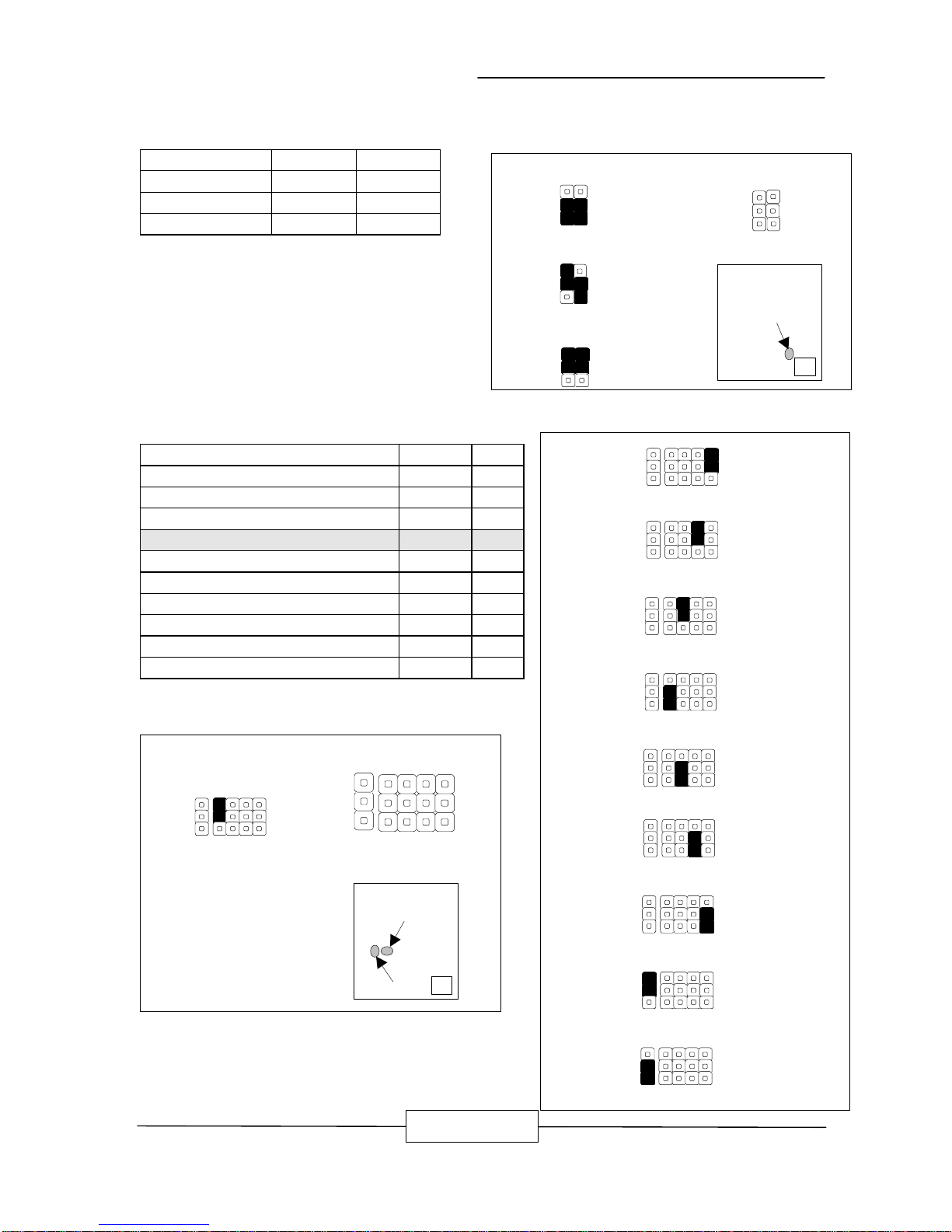
l JP7, JP8 : Select L2 Cache Size
L2 Cache JP7 JP8
128K 2-3 2-3
256K 2-3 1-2
512K 1-2 1-2
l JP14, JP15 : Select Watch-Dog Timer
Time Out Period JP14 JP15
0.5 sec 1-5 OFF
1 sec 2-6 OFF
2 sec 3-7 OFF
4 sec (Default ) 4-8 OFF
8 sec 8-12 OFF
16 sec 7-11 OFF
32 sec 6-10 OFF
64 sec 5-9 OFF
128 sec OFF 1-2
256 sec OFF 2-3
33
1
1
JP7JP8
JP7
JP8
128K L2 Cache
33
11
JP7
JP8
256K L2 Cache
3
3
1
1
JP7JP8
512K L2 Cache
1
1
JP7
JP8
4 Sec (Default)
JP14
4 3 2
L
H
12
11
10
3
JP15
JP15
JP14
JP14
L
H
3
2
1
4
9
101211
1
3
JP15
JP15
1
3
1
3
1
JP14
L
H
2
4
9
101211
1
3
JP15
0.5 Sec
JP14
L
H
3
2
4
9
101211
1
3
JP15
1 Sec
JP14
L
H
2
1
4
9
101211
3
JP15
2 Sec
JP14
L
H
3
2
1
4
9
101211
1
3
JP15
8 Sec
JP14
L
H
3
2
1
4
9
101211
1
3
JP15
16 Sec
JP14
L
H
3
2
1
4
9
101211
1
3
JP15
32 Sec
JP14
L
H
3
2
1
4
9
101211
1
3
JP15
64 Sec
JP14
L
H
3
2
1
4
9
101211
1
3
128 Sec
L
H
3
2
1
4
9
101211
1
3
JP15
256 Sec
Page 19
JUMPER SETTINGS AND CONNECTORS
TF-486 / 13
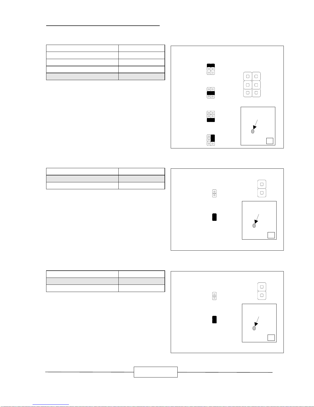
JP16 : Select Disk On Chip ( Flash Disk ) Address
Flash Disk Address JP16
C8000~CFFFF 1-2
D0000~D7FFF 3-4
D8000~DFFFF 5-6
Default 2-4
l S2 : Clear CMOS Jumper
Clear CMOS Jumper S2
Normal (Default ) OFF
Clear CMOS 1-2
l SMI1 : External SMI Function Switch
SMI Function SMI1
Disable OFF
Enable ON
JP16
D0000~D7FFF
D8000~DFFFF
C8000~CFFFF
1 2
5
6
6
JP16
1
3
5
4
2
Spare Jumper
JP16
S2
Clear CMOS
Normal
2
1
S2
2
1
S2
SMI1
Enable
Disable
2
1
SMI1
2
1
SMI1
Page 20
JUMPER SETTINGS AND CONNECTORS
TF-486 / 14
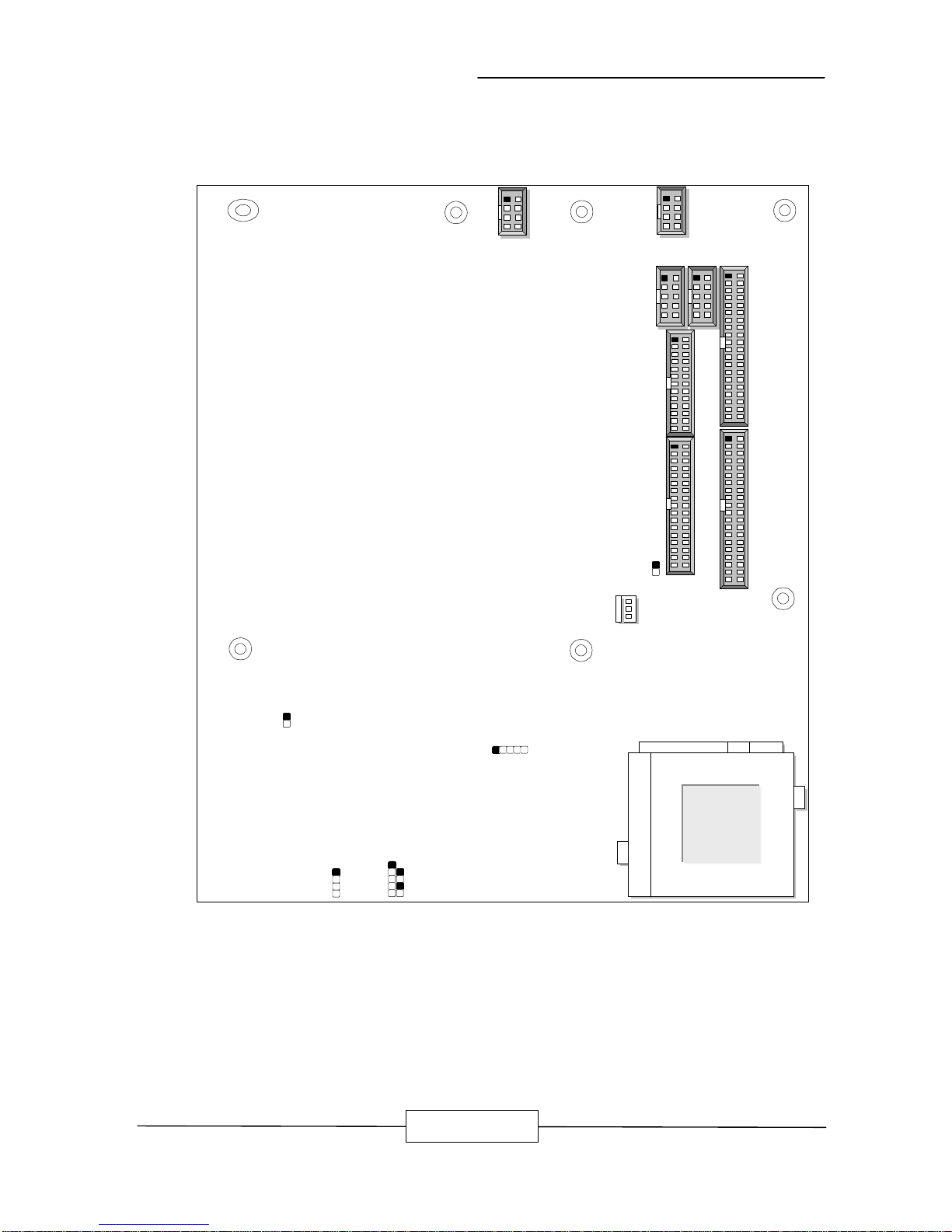
2.7 I/O CONNECTOR LOCATION FOR TF-486
TF-486
FAN1
COM1
J1
1
PIDE1
PIDE2
1
4
5
J4
J5
J2
J3
1
COM2
PRT1
FDC1
PMS1
PKB1
J6
JP13
1
5
Page 21

JUMPER SETTINGS AND CONNECTORS
TF-486 / 15
2.8 I/O CONNECTOR SUMMARY FOR TF-486
CONNECTOR FUNCTION
J1 HDD LED
J2 Turbo Switch
J3 Turbo LED
J4 Power LED & Key Lock
J5 Speaker Connector
J6 Reset Switch
COM1 COM1 Connector (Header)
COM2 COM2 Connector (Header)
FAN1 FAN Power Connector
JP13 Alternate IrDA Connector
PKB1 External Keyboard Connector (Header)
PMS1 External PS/2 Mouse Connector (Header)
PIDE1/PIDE2 EIDE Interface Connector ( Header )
FDC1 Floppy Interface Connector ( Header )
PRT1 Parallel Port Connector ( Header )
Page 22
JUMPER SETTINGS AND CONNECTORS
TF-486 / 16
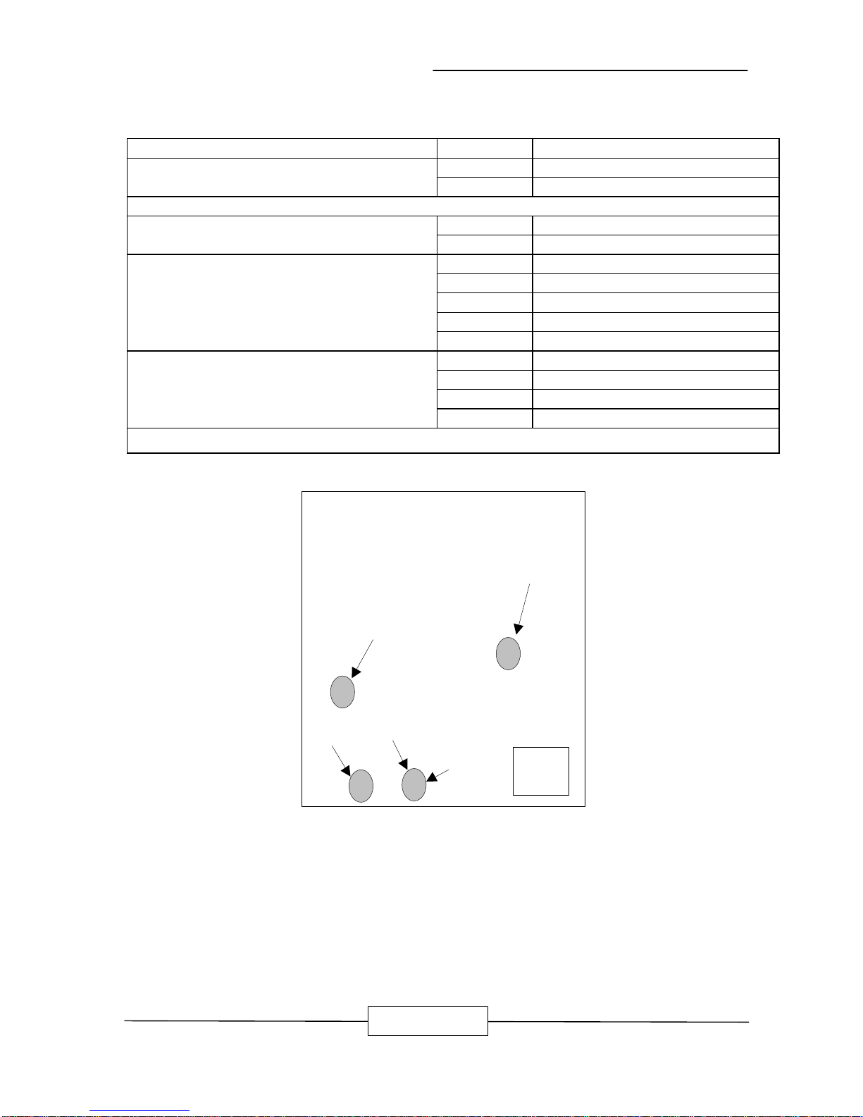
2.9 SYSTEM STATUS INDICATE AND CONTROL CONNECTORS
CONNECTOR PIN NO. DESCRIPTION
1 V
CC
J1 : HDD LED
2 Ground
J2 : Turbo Switch
1 V
CC
J3 : Turbo Switch
2 Ground
1 Power LED V
CC
2 NC
3 Power LED Ground
4 Key Lock Signal
J4 : Power LED & Key Lock
5 Ground
1 V
CC
2 NC
3 NC
J5 : Speaker Connector
4 Signal
J6 : Reset Switch
J1
J2
J3
J6
J5
J4
Page 23
JUMPER SETTINGS AND CONNECTORS
TF-486 / 17
2.10 I/O CONNECTORS DESCRIPTION
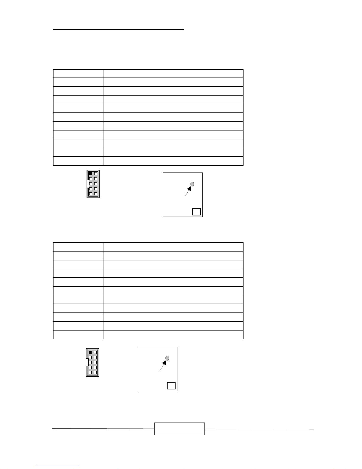
l COM1 : Connector ( Header )
PIN NO. DESCRIPTION
1 DCD1#
2 SIN1
3 SOUT1
4 DTR1#
5 Ground
6 DSR1#
7 RTS1#
8 CTS1#
9 RI1#
10 NC
l COM2 : Connector ( Header )
PIN NO. DESCRIPTION
1 DCD2#
2 SIN2
3 SOUT2
4 DTR2#
5 Ground
6 DSR2#
7 RTS2#
8 CTS2#
9 RI2#
10 NC
1 2
9
10
COM1
COM1
1 2
9
10
COM2
COM2
Page 24
JUMPER SETTINGS AND CONNECTORS
TF-486 / 18
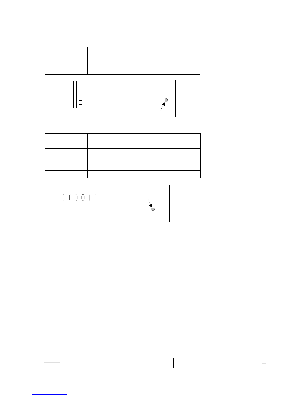
l FAN1 : FAN Connector
PIN NO. DESCRIPTION
1 Ground
2 +12V
3 NC
l JP13 : Alternate IrDA Connector
PIN NO. DESCRIPTION
1 VCC
2 NC
3 IR_RX
4 Ground
5 IR_TX
FAN1
1
3
FAN1
JP13
1 5
JP13
Page 25
JUMPER SETTINGS AND CONNECTORS
TF-486 / 19
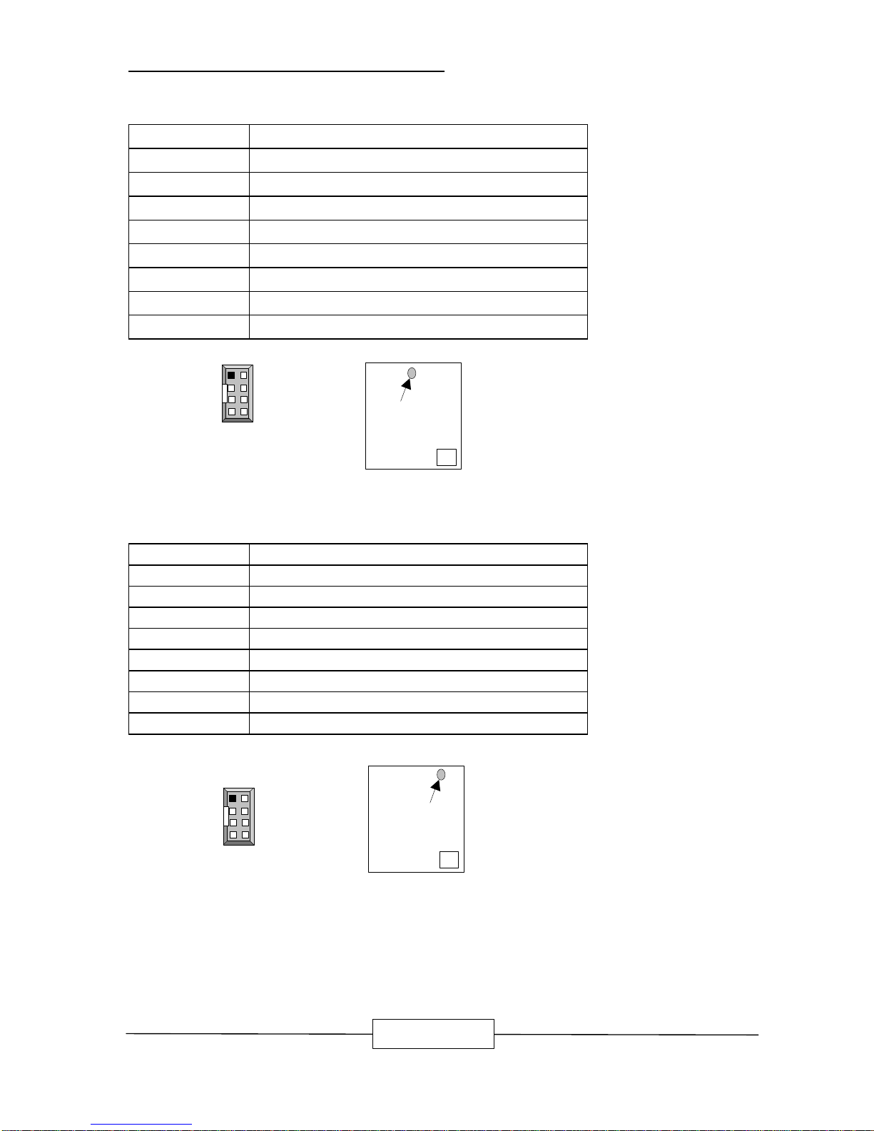
l PKB1 : Keyboard Connector
PIN NO. DESCRIPTION
1 Keyboard Clock
2 Ground
3 NC
4 Keyboard Data
5 NC
6 NC
7 NC
8 Vcc
l PMS1 : PS/2 Mouse Connector ( Header )
PIN NO. DESCRIPTION
1 PS/2 Mouse Clock
2 Ground
3 NC
4 PS/2 Mouse Data
5 NC
6 NC
7 NC
8 Vcc
l
2
1
PKB1
8
7
PKB1
21
PMS1
8
7
PMS1
Page 26
JUMPER SETTINGS AND CONNECTORS
TF-486 / 20
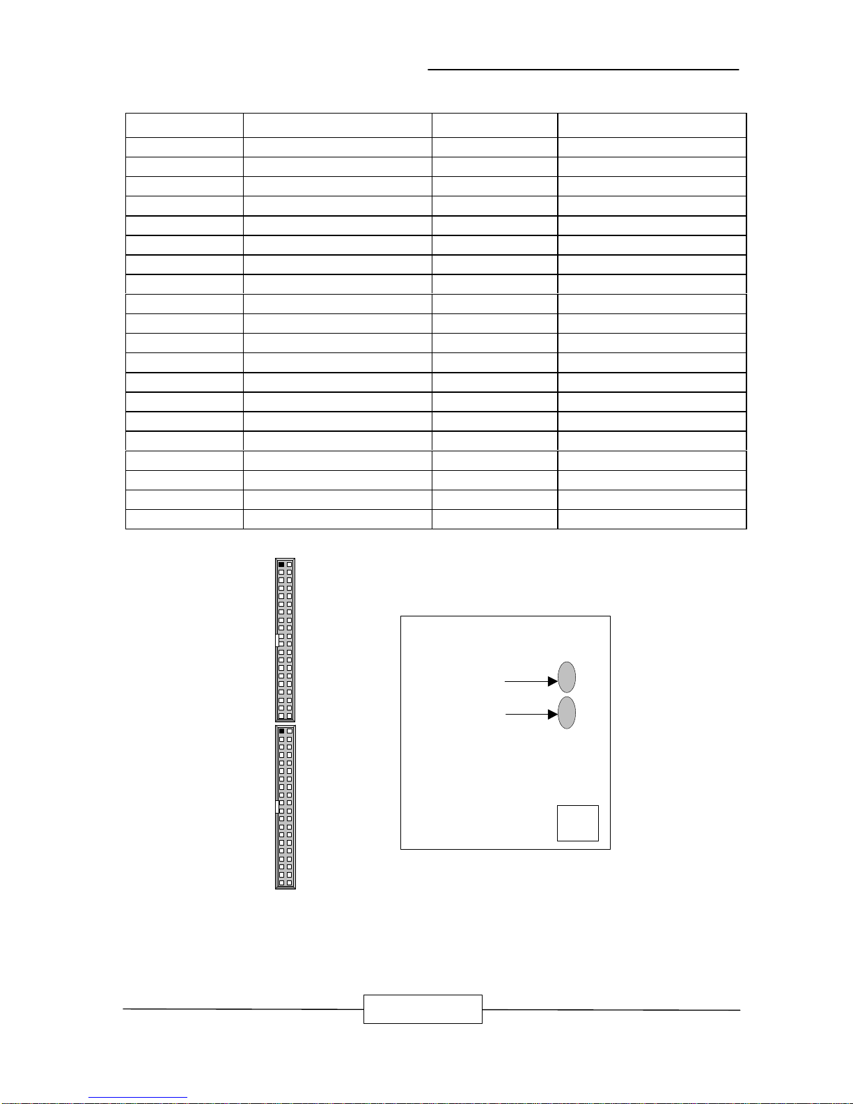
PIDE1 / PIDE2 : EIDE Interface Connector ( Header )
PIN NO.
DESCRIPTION
PIN NO.
DESCRIPTION
1 Reset # 2 Ground
3 Data 7 4 Data 8
5 Data 6 6 Data 9
7 Data 5 8 Data 10
9 Data 4 10 Data 11
11 Data 3 12 Data 12
13 Data 2 14 Data 13
15 Data 1 16 Data 14
17 Data 0 18 Data 15
19 Ground 20 NC
21 NC 22 Ground
23 IOW# 24 Ground
25 IOR# 26 Ground
27 IOCHRDY 28 NC
29 NC 30 Ground
31 Interrupt 32 HDIO16J
33 SA1 34 NC
35 SA0 36 SA2
37 HDC CS0# 38 HDC CS1#
39 HDD Active 40 Ground
PIDE1
39
40
PIDE2
1
2
39
40
PIDE1
PIDE2
2
1
Page 27
JUMPER SETTINGS AND CONNECTORS
TF-486 / 21
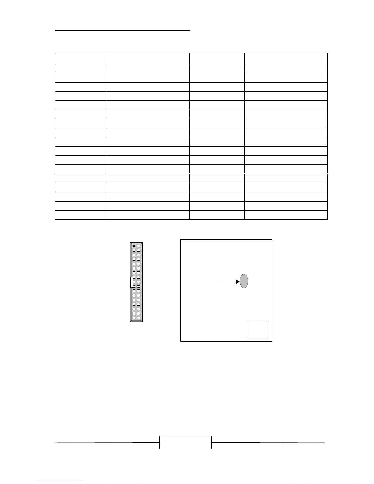
FDC1 : Floppy Interface Connector ( Header )
PIN NO.
DESCRIPTION
PIN NO.
DESCRIPTION
1 Ground 2 Density Select
3 Ground 4 NC
5 Ground 6 DS1
7 Ground 8 Index #
9 Ground 10 Motor Enable A#
11 Ground 12 Drive Select B#
13 Ground 14 Drive Select A#
15 Ground 16 Motor Enable B#
17 Ground 18 Direction #
19 Ground 20 Step #
21 Ground 22 Write Data #
23 Ground 24 Write Gate #
25 Ground 26 Track 0#
27 Ground 28 Write Protect
29 NC 30 Read Data #
31 Ground 32 Head Side Select #
33 NC 34 Disk Change #
FDC1
33
34
2
1
FDC1
Page 28
JUMPER SETTINGS AND CONNECTORS
TF-486 / 22
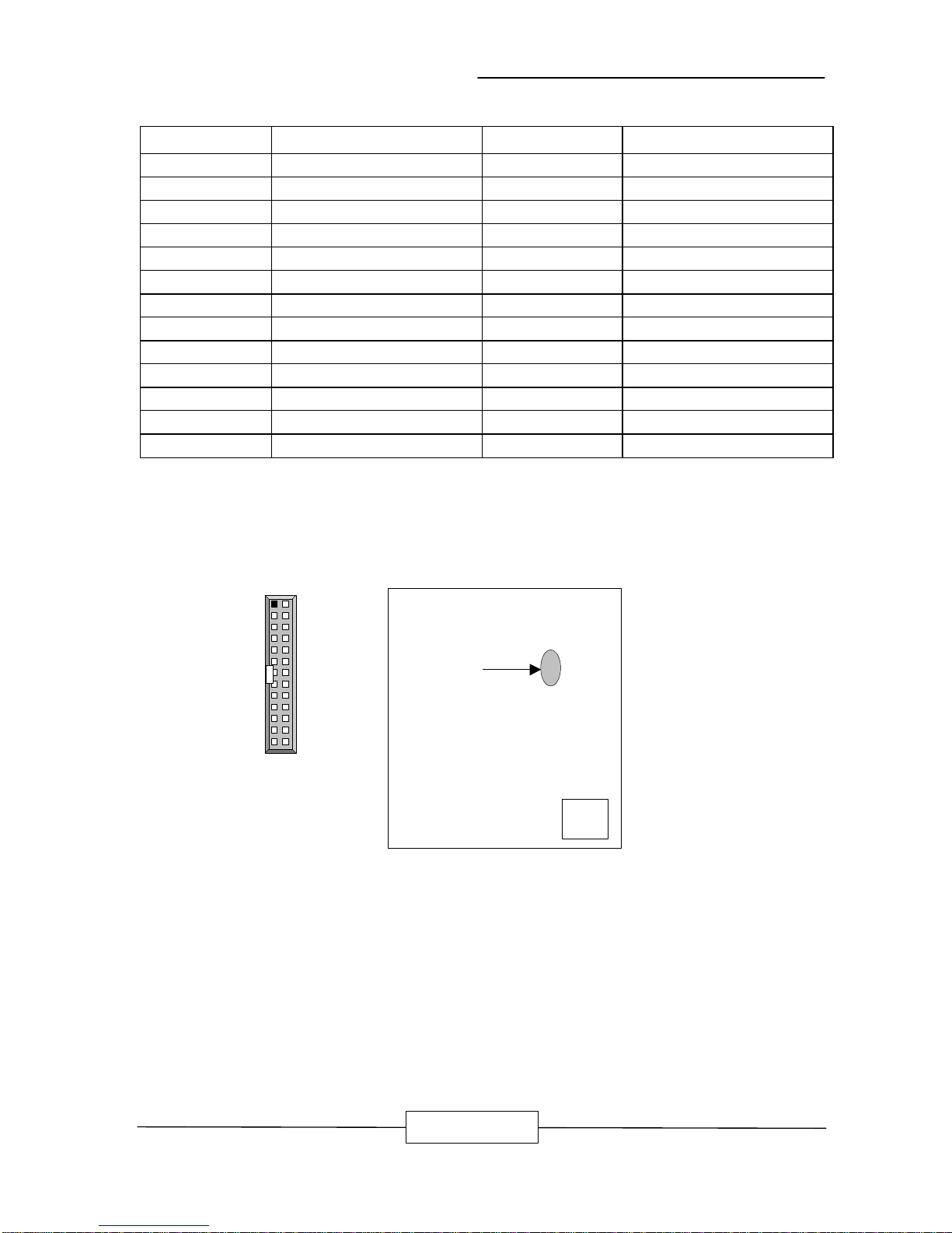
PRT1 : Parallel Port Connector ( Header )
PIN NO.
DESCRIPTION
PIN NO.
DESCRIPTION
1 Strobe # 2 Auto Form Feed
3 Data 0 4 Error #
5 Data 1 6 Initialize #
7 Data 2 8 Printer Select IN #
9 Data 3 10 Ground
11 Data 4 12 Ground
13 Data 5 14 Ground
15 Data 6 16 Ground
17 Data 7 18 Ground
19 Acknowledge # 20 Ground
21 Busy 22 Ground
23 Paper Empty 24 Ground
25 Printer Select 26 NC
PRT1
25
26
2
1
PRT1
Page 29

TF-486 / 23
CHAPTER 3.
AWARD BIOS SETUP
The Basic Input / Output System (BIOS) is a program that takes care of the basic level of
communication between the processor and peripherals. In addition, the BIOS also
contains codes for various advanced features found in the system board. Award' s ROM
BIOS provides a built-in Setup program that allows user to modify the basic system
configuration and settings. The modified data will be stored in a battery-backed CMOS
RAM so that the data will be retained even when the power is turned off. In general,
the information saved in the CMOS RAM stay unchanged unless there is configuration
change in the system, such as hard drive replacement or new equipment is installed.
3.1 RUNNING AWARD BIOS
The Setup Utility is stored in the BIOS ROM. When the power of the computer system
is turned on, a screen message appears to give you an opportunity to call up the Setup
Utility; while the BIOS will enter the Power On Self Test (POST) routines. The POST
routines perform various diagnostic checks while initializing the board hardware. If the
routines encounter an error during the tests, the error will be reported in either of the two
different ways, you may hear a series of short beeps or see an error message on the
screen display. There are two kinds of error: fatal or non-fatal. The system can
usually continue to boot up sequence with the non-fatal errors. Non-fatal error
messages usually appear on the screen along with the following instructions:
“ Press <F1> to RESUME ”
Write down the message and press the F1 key to continue the boot up sequence. After
the POST routines are completed, the following message appears:
“ Press DEL to enter SETUP ”
Entering Setup
Turn on the power of the computer system and press <Del> immediately. If you don’ t
have the chance to respond, reset the system by simultaneously typing the <Ctrl>, <Alt>
and <Delete> keys, or by pushing the ‘ Reset ’ button on the system cabinet. You can
also restart by turning the system OFF then ON.
Page 30
BIOS SETUP
TF-486 / 24
3.2 CMOS SETUP UTILITY
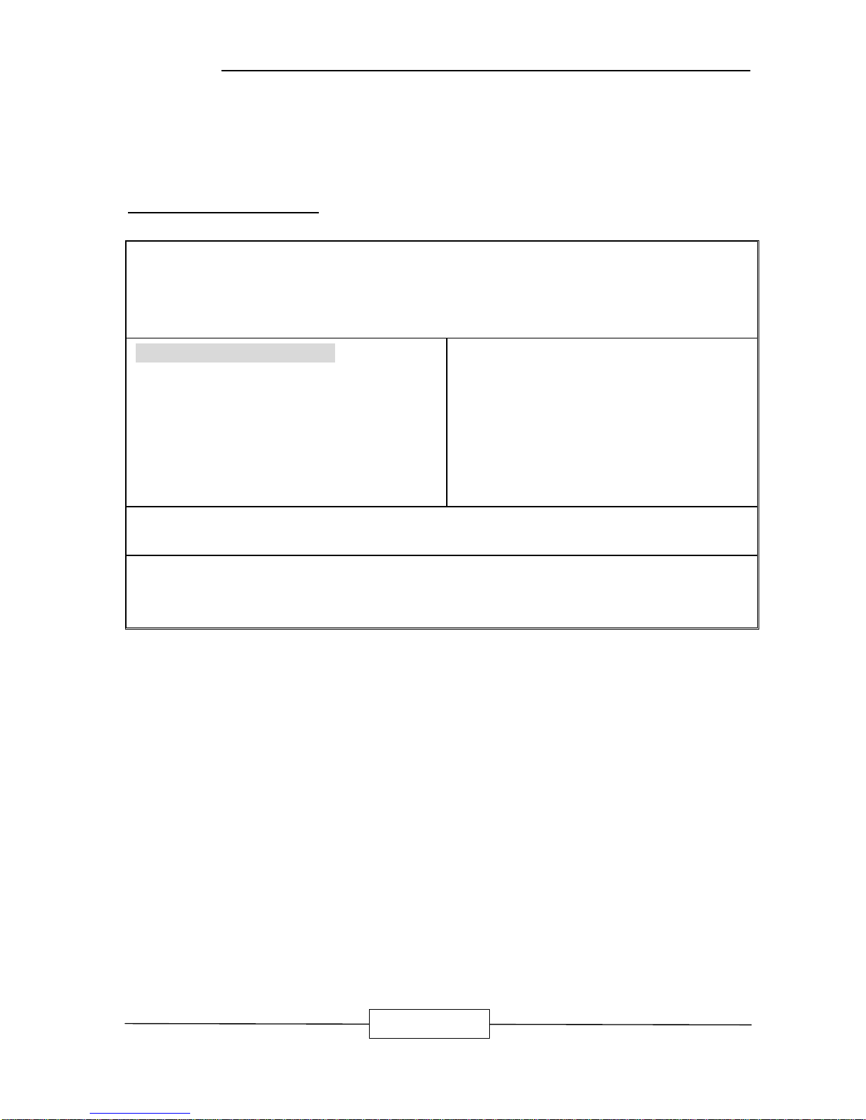
To access the AWARD BIOS SETUP program, press the <DEL> key. The screen
display will appears as :
Main Program Screen
ROM PCI / ISA BIOS (2A4KDL7F)
CMOS SETUP UTILITY
AWARD SOFTWARE, INC.
STANDARD CMOS SETUP
BIOS FEATURES SETUP
CHIPSET FEATURES SETUP
POWER MANAGEMENT SETUP
PCI CONFIGURATION SETUP
LOAD BIOS DEFAULTS
LOAD SETUP DEFAULTS
INTEGRATED PERIPHERALS
SUPERVISOR PASSWORD
USER PASSWORD
IDE HDD AUTO DETECTION
HDD LOW LEVEL FORMAT
SAVE & EXIT SETUP
EXIT WITHOUT SAVING
ESC : Quit á â à : Select Item
F10 : Save & Exit Setup (Shift) F2 : Change Color
Time, Date, Hard Disk Type...
This screen provides access to the utility‘ s various functions.
Listed below are explanations of the keys displayed at the bottom of the screen:
<ESC> : Exit the utility.
á â à
: Use arrow keys á â à to move cursor to your desired selection.
<F10> : Saves all changes made to Setup and exits program.
<Shift><F2> : Changes background and foreground colors.
Page 31

BIOS SETUP
TF-486 / 25
3.3 STANDARD CMOS SETUP
When you select the “STANDARD CMOS SETUP” on the main program, the screen
display will appears as :
Standard CMOS Setup Screen
ROM PCI / ISA BIOS(2A4KDL7F)
STANDARD CMOS SETUP
AWARD SOFTWARE, INC.
Date
Time
(mm : dd : yy)
(hh : mm : ss)
:Fri, May 21 1999
: 10 : 2 0 : 10
HARD DISKS TYPE SIZE CYLS. HEAD PRECOMP LANDZ SECTOR MODE
Primary Master : Auto 0M 0 0 0 0 0 AUTO
Primary Slave : Auto 0M 0 0 0 0 0 AUTO
Secondary Master : Auto 0M 0 0 0 0 0 AUTO
Secondary Slave : Auto 0M 0 0 0 0 0 AUTO
Drive A
Drive B
Floppy 3
: 1.44M, 3.5 in.
: None
Mode Support : Disabled
Base Memory :
Extended Memory :
Other Memory :
640K
64512K
384K
LCD&CRT
Halt On
: Auto
: All Errors
Total Memory : 65536K
ESC : Quit á â à : Select Item PU / PD / + / - : Modify
F1 : Help (Shift ) F2 : Change Color
The Standard CMOS Setup utility is used to configure the following components such as
date, time, hard disk drive, floppy drive, display, and memory. Once a field is
highlighted, on-line help information is displayed in the left bottom of the Menu screen.
Set Date : Month, Date, Year.
Set Time : Hour, Minute and Second. Use 24 Hour clock format (for p.m. time, add 12
to the hour number, you would enter 4:30p.m. as 16:30).
Page 32

BIOS SETUP
TF-486 / 26
Hard Disks : There are four hard disks listed: “Primary Master”, “Primary Slave”,
“Secondary Master” and “Secondary Slave”. For each IDE channel, the first device is
the “Master” and the second device is “Slave”. Hard disk types from 1 to 45 are the
standard ones. To select or change the configuration, move the cursor to the desired
position and press <Page Up> or <Page Down> to change the option : (1) Press “Auto”
for IDE HDD auto detection, (2) Press “User” for user definable, and Press “None” for not
installed (e.g. SCSI). There are six categories of information that you must enter for a
HDD: “CYLS.” for (number of cylinders), “HEADS” for (number of heads), “PRECOMP”
for (write pre-compensation), “LANDZ” for (landing zone), “SECTOR” for (number of
sectors) and ”MODE“ for (Normal, LBA, LARGE and AUTO). The hard disk vendor‘ s or
system manufacturer’ s documentation should provide you with the drive specifications.
For an IDE hard drive, you can set “TYPE” to “Auto” or use the “IDE HDD AUTO
DETECTION” utility in the main program screen to enter the drive specifications.
Here is a brief explanation of drive specifications:
l Type : The BIOS contains a table of pre-defined drive types. Each defined
drive type has specified number of cylinders, number of heads, write compensation
factor, landing zone, and number of sectors. Drives whose specifications do not
accommodate any pre-defined type are classified as type USER.
l Size : Disk drive capacity (approximate). Note that this size is usually slightly
greater than the size of a formatted disk given by a disk checking program.
l Cyls : Number of cylinders.
l Head : Number of heads.
l Precomp : Write pre-compensation cylinder
l Landz : Landing zone.
l Sector : Number of sectors.
l Mode : Auto, Normal, Large, or LBA.
• Auto: The BIOS automatically determines the optimal mode.
• Normal: Maximum number of cylinders, heads, and sectors supported are 1024,
16, and 63.
• Large: For drives that do not support LBA and have more than 1024 cylinders.
• LBA (Logical Block Addressing): During drive accesses, the IDE controller
transforms that data address described by sector, head, and cylinder number
into physical block address, significantly improving data transfer rates. For
drives that greater 1024 cylinders.
Page 33

BIOS SETUP
TF-486 / 27
There are four hard disks listed: “Primary Master”, “Primary Slave”, “Secondary Master”
and “Secondary Slave”. For each IDE channel, the first device is the “Master” and the
second device is “Slave”. Hard disk types from 1 to 45 are the standard one. To
select or change the configuration, move the cursor to the desired position and press
<Page Up> or <Page Down> to change the option.
The AWARD BIOS supports three HDD modes: NORMAL, LBA and LARGE.
NORMAL mode : This is a Generic Access mode in which neither the BIOS nor the IDE
controller will make any transformation during the accession. The maximum HDD size
is supported by the NORMAL mode that is 528 Megabytes.
LBA mode : This is a Logical Block Addressing mode which is a HDD accessing method
to overcome the 528 Megabytes restriction. The number of cylinders, heads and
sectors that are shown in setup may not be the physical number contained in the HDD.
During the HDD accessing, the IDE controller will transform the logical address that is
described by the cylinder, head and sector numbers into its own physical address as
contained inside the HDD. The maximum HDD size that is supported by the LBA mode
is 8.4 Gigabytes.
LARGE mode : Some IDE HDD contains more than 1024 cylinders without the LBA
support. This access mode tricks DOS (or other OS) with the number of cylinders that
is less than 1024 by dividing it by 2. At the same time, the number of heads is multiplied
by 2. A reverse transformation process will be made inside INT13H in order to access
to the right HDD address. The maximum HDD size that is supported by the LARGE
mode is 1 Gigabytes.
Note : 1. To support LBA or LARGE mode, there are softwares located in the AWARD
HD Service Routine“INT13H”. It may fail to access a HDD with LBA or
LARGE modes selected if you are running under an Operating System that
replaces the whole INT13H service routine.
2. Entering incorrect drive specifications will result in a hard disk drive that will
function improperly or no function at all.
Page 34
BIOS SETUP
TF-486 / 28
Drive A and Drive B : Select the correct specifications for the diskette drive(s) installed
in the computer.
None No diskette drive installed
360K, 5.25 in 5-1/4 inch PC-type standard drive; 360 kilobyte capacity
1.2M, 5.25 in 5-1/4 inch AT-type high-density drive; 1.2 megabyte capacity
720K, 3.5in 3 1-2 inch double-sided drive; 720 kilobyte capacity
1.44M, 3.5 in 3 1-2 inch double-sided drive; 1.44 megabyte capacity
2.88M, 3.5 in 3 1-2 inch double-sided drive; 2.88 megabyte capacity
Note : 1. Not Installed could be used as an option for diskless workstations..
2. Highlight the listing after each drive name and select the appropriate entry.
LCD&CRT : Select display type.
Auto Automatic detects display type
CGA 40 Color Graphics Adapter, power up in 40 column mode
CGA 80 Color Graphics Adapter, power up in 80 column mode
MONO Monochrome adapter, includes high resolution monochrome adapter
Halt On : During the power-on-self-test (POST), the computer stops if the BIOS detects
a hardware error. You can tell the BIOS to ignore certain errors POST and continue the
boot-up process. These are the selections:
No errors Whenever the BIOS detects a non-fatal error the system will not be
stopped and you will be prompted
All errors The system boot will be stopped for any error that may be detected.
All, But Keyboard The system boot will not stop for a keyboard error ; it will stop for all
Other errors.
All, But Diskette The system boot will not stop for a disk error ; it will stop for all other
Errors.
All, But Disk/Key The system boot will not stop for a keyboard or disk error ; it will stop
for all other errors.
Page 35

BIOS SETUP
TF-486 / 29
Memory : You cannot change any values in the Memory fields; they are only for your
information. The fields show the total installed random access memory (RAM) and
amounts allocated to base memory, extended memory, and other (high) memory. RAM
is counted in kilobytes (KB: approximately one thousand bytes) and megabytes (MB:
approximately one million bytes).
RAM is the computer’ s working memory, where the computer stores programs and data
currently being used, so they are accessible to the CPU. Modern personal computers
may contain up to 64MB, 128MB, or more.
l Base Memory : Typically 640KB. Also called conventional memory. The DOS
operating system and conventional applications use this area.
l Extended Memory : Above the 1-MB boundary. Early IBM personal computers
could not use memory above 1MB, but current PCs and their software can use
extended memory.
l Other Memory : Between 640KB and 1MB; called High memory. DOS may load
terminate-and-stay-resident (TSR) programs, such as device drivers, in this area, to
free as much conventional memory as possible for applications. Lines in your
CONFIG.SYS file that start with LOADHIGH load programs into high memory.
Page 36

BIOS SETUP
TF-486 / 30
3.4 BIOS Features Setup
When you select the “BIOS FEATURES SETUP” on the main program, the screen
display will appears as:
BIOS Features Setup Screen
ROM PCI / ISA BIOS (2A4KDL7F)
BIOS FEATURES SETUP
AWARD SOFTWARE, INC
Virus Warning :Disabled Video BIOS Shadow : Enabled
CPU Internal Cache :Enabled C8000-CFFFF Shadow : Disabled
External Cache :Enabled D0000-D7FFF Shadow : Disabled
Quick Power On Self Test :Enabled D8000-DFFFF Shadow : Disabled
Boot Sequence :A,C,SCSI
Swap Floppy Drive :Disabled
Boot Up Floppy Seek :Disabled
Boot Up NumLock Status :On
Boot Up System Speed :High
Gate A20 Option :Fast
Typematic Rate Setting :Disabled
Typematic Rate (Chars/Sec) :6
Typematic Delay (Msec) :250
Security Option :Setup
PCI/VGA Palette Snoop :Disabled ESC : Quit áâà : Select Item
OS Select For DRAM >64MB :Non-OS2 F1 : Help PU /PD /+/ - : Modify
F5 : Old Values (Shift) F2 : Color
F6 : Load BIOS Defaults
F7 : Load Setup Defaults
The following explains the options for each of the features as listed in the above menu:
Virus Warning : The default setting of the Virus Warning is “Disabled”. When it is
enabled, any attempt to write the boot sector and partition table will halt the system and
cause a warning message to appear. If this happens, you can use an anti-virus utility
on a virus free, bootable floppy diskette to reboot, to clean and to investigate your
system.
Page 37

BIOS SETUP
TF-486 / 31
CPU Internal Cache : The default setting is “Enabled”. This setting enables the CPU
internal cache.
External Cache : The default setting is “Enabled”. This setting enables the external
cache.
Quick Power On Self Test : The default setting is “Enabled”. This speeds up the
Power On Self Test (POST) by skipping some items that are normally checked during the
full POST. If your system is functioning normally, you can choose this feature to speed
the booting process.
Boot Sequence : The default setting is “A:,C SCSI”; the other options are “C,A,SCSI”;
“C,CDROM,A”; “CDROM,C,A”; “D,A,SCSI”; “E,A,SCSI”; “F,A,SCSI”; “SCSI,A,C”;
“SCSI,C,A”; “C only”; and “LS/ZIP,C”. This setting determines where the computer
looks first for an operating system, the hard disk, or the floppy disk, … or other. The
BIOS will load the operating system from the disk drives in the sequence as selected
here.
Swap Floppy Drive : The default setting is “Disabled”. This setting gives you an option
to swap A and B floppy disks. Normally, the floppy drive A is the one at the end of the
cable and drive B is at the other end. If you set this option to “Enabled”, the Drive A will
function as Drive B, and vice-versa under the DOS.
Boot Up Floppy Seek : The defaults setting is “Disabled”. When enabled, the BIOS
will check whether there is a floppy disk drive installed.
Boot Up Numlock Status : The default setting is “On”. If set “Off”, the cursor controls
will function on the numeric keypad.
Boot Up System Speed : The default setting is “High”. This sets the CPU speed at boot
up.
Gate A20 Option : The default setting is “Fast”. This is the optimal setting for the CPU
card. The other option is “Normal”.
Typematic Rate Setting : The default setting is “Disabled”. If enabled, you can set the
typematic rate and typematic delay.
Page 38

BIOS SETUP
TF-486 / 32
Typematic Rate (Chars/Sec) : This setting controls the speed at which the system
registers the repeated keystrokes. The choices range from 6 to 30 Chars/Sec. The
default setting is “6” Chars/Sec.
Typematic Delay (Msec) : This setting controls the time between the display of the first
and second characters. There are four delay choices: 250ms, 500ms, 750ms and
1000ms. The default setting is “250” ms.
Security Option : This setting controls the password in the main screen. The options
are “Setup” and “System”. Select “Setup” and it will protect the Setup Utility settings
from being tampered with. Select “System” if you want to use password feature every
time the system boots up. The default setting is “Setup”. You can create your password
by using the “SUPERVISOR/USER PASSWORD” utility on the main program screen.
PCI/VGA Palette Snoop : The default setting is “Disabled”. Set to “Enable” if any ISA
adapter card installed requires VGA palette snooping.
OS Select For DRAM > 64MB : The default setting is “Non-OS2”. Set to “OS2” if the
system memory size is greater than 64MB and the operating system is OS/2.
Video BIOS Shadow : The default setting is “Enabled” which will copy the VGA display
card BIOS into system DRAM to improve performance.
C8000-CFFFF Shadow to D8000-DFFFF Shadow : The default setting for the shadow
feature is “Disabled”. When enabled, the ROM with the specific address is copied into
system DRAM. It will also reduce the size of memory available to the system. After
you have made your selection in the BIOS FEATURES SETUP, press the <ESC> key to
go back to the main program screen.
Page 39

BIOS SETUP
TF-486 / 33
3.5 CHIPSET FEATURES SETUP
When you select the “CHIPSET FEATURES SETUP” on the main program, the screen
display will appears as:
Chipset Features Setup Screen
ROM PCI / ISA BIOS (2A4KDL7F)
CHIPSET FEATURES SETUP
AWARD SOFTWARE, INC.
AUTO Configuration : Enabled Special Functions Port : Disable
Touch Controller IRQ : Disable
AT-BUS Clock : CLK/4
DRAM Read Timing : Normal
DRAM Write Timing : Normal
SRAM Read Timing : 3-1-1-1
SRAM Write Timing : 0 Wait
Hidden Refresh : Disable
Memory Hole (15M – 16M) : Disable
ISA I/O Recovery : Enable
Fast-Back-to-Back : Enable
ESC : Quit áâà: Select Item
F1 : Help PU /PD /+/ - : Modify
F5 : Old Values (Shift) F2 : Color
F6 : Load BIOS Defaults
F7 : Load Setup Defaults
This section describes features of the board’ s chipset. All the entries on the screen are
automatically configured. However, you can change it according to your operating
environment.
Auto Configuration : The default setting is “Enabled” which will optimize DRAM timing
automatically depending on whether the DRAM used is either 70ns or 60ns. The other
option is “Disabled” which allows you to change DRAM timing manually.
Page 40

BIOS SETUP
TF-486 / 34
AT-BUS Clock : You can set the speed of the AT bus in terms of the CPU clock speed,
or at the fixed speeds of 7.16M Hz.
DRAM Read / Write Timing : Timing that the system uses when reading from and
writing to DRAM. Do not reset from the manufacturer default value.
SRAM Reading Timing : These SRAM timing numbers are the pattern of cycles the
CPU uses to read data from the cache. Do not reset this option from its default.
SRAM Writing Timing : If necessary, you can insert a wait state in the SRAM write
cycle.
Hidden Refresh : When Disabled, DRAM is refreshed by IBM AT methodology, using a
CPU cycles for each refresh. When hidden refresh is Enabled, the DRAM controller
seeks the most opportune moment for a refresh, regardless of CPU cycles, with least
disruption of system activity and least performance penalty. Hidden refresh is faster
and more efficient, and it also allows the CPU to maintain the status of the DRAM even if
the system goes into a power management “suspend” mode.
Memory Holes (15M-16M) : The default setting is “Disable”. Set to “Enable” means
that when the system memory size is equal to or greater than 16M bytes, the physical
memory address from 15M to 16M will be passed to PCI or ISA and there will be 1M
Bytes hole in your system memory. This option is designed for some OS with special
add-on cards which need 15M-16M memory space.
ISA I/O Recovery : The CPU and local bus are much faster than industry standard
architecture (ISA) input / output (I/O) bus. Select Enabled to allow additional time for
I/O devices to respond to the system. Otherwise, data could be lost. If all your I/O
devices are capable of fast I/O, selecting Disabled can speed up processing.
Fast-Back-to-Back : When Enable, consecutive write cycles targeted to the same slave
become fast back-to-back on the PCI bus.
Special Functions Port : Select Touch Screen I/O ports address.
Touch Controller IRQ : Select Touch Screen IRQ.
Page 41

BIOS SETUP
TF-486 / 35
3.6 Power Management Setup
The “Power Management Setup” controls the CPU card‘ s “Green” features.
Selecting “POWER MANAGEMENT SETUP” and the Screen appears as ...
ROM PCI / ISA BIOS (2A4KDL7F)
POWER MANAGEMENT SETUP
AWARD SOFTWARE, INC.
Power Management : User Define IRQ5 (LPT 2) : ON
PM Control by APM : Yes IRQ6 (Floppy Disk) : ON
Video Off Option : Susp, Stby -> Off IRQ7 (LPT 1) : ON
Video Off Method : V/H SYNC+ Blank IRQ8 (RTC Alarm) : OFF
MODEM Use IRQ : 3 IRQ9 (IRQ2 Redir) : ON
IRQ10 (Reserved) : OFF
** PM Timers ** IRQ11 (Reserved) : OFF
HDD Power Down : Disable IRQ12 (PS/2 Mouse) : ON
Doze Mode : 30 Sec IRQ13 (Coprocessor) : OFF
Standy Mode : 30 Sec IRQ14 (Hard Disk) : ON
Suspend Mode : 30 Sec IRQ15 (Reserved) : OFF
** PM Events **
VGA : OFF
FDD (3FXh) : ON
LPT & COM : LPT/COM ESC : Quit áâà : Select Item
HDD (1FXh) : ON F1 : Help PU /PD/+/- : Modify
NMI : OFF F5 : Old Values ( Shift ) F2 : Color
IRQ3 (COM 2) : ON F6 : Load BIOS Defaults
IRQ4 (COM 1) : ON F7 : Load Setup Defaults
Power Managemant : This setting controls the System Doze Mode, Standby Mode and
Suspend Mode Timer features. There are four options:
User Define : Allows you to customize all power saving timer features.
Optimize : This is the recommended setting for general use.
Test/Demo : This is for test/demonstration purpose.
Disable : Disable the power management features.
PM Control by APM : The default setting is “ No ”. If set to “ Yes ”, system BIOS will
wait for APM‘ s prompt before it enters any PM mode.
Note : If your system power management is controlled by APM and there is a task
running, the APM will not prompt the BIOS to enter any power saving mode after time
out.
Page 42

BIOS SETUP
TF-486 / 36
Video Off Method : This setting controls the Video off method in power saving mode.
The default setting is “ V/H SYNC+Blank ”. This setting disables V/H SYNC signals and
blanks the screen in power saving mode. Other options are “ Blank Screen ” and
“ DPMS ”.
Doze Mode : Options are from “ 1 Minute ” to “ 1 Hour ” and “ Disable ”. The system
speed will change from turbo to slow if no Power Management events occur for a
specified length of time. Full power function will return when a Wake-Up event is
detected.
Standby Mode : Options are from “ 1 Minute ” to “ 1 Hour ” and “ Disable ”. The system
speed will change from turbo to slow and the video signal will be suspended if no Power
Management events occur for a specified length of time. Full power function will return
when a Wake-Up event is detected.
Suspend Mode : Option are from “ 1 Minute ” to “ 1 Hour ” and “ Disable ”. The CPU
clock will be stopped and the video signal will be suspended if no Power Management
events occur for a specified length of time. Full power function will return when a
Wake-Up event is detected.
HDD Power Down : Options are from “ 1 Minute ” to “ 15 Minutes ” and “ Disable ”. The
IDE hard drive will spin down if it is not accessed within a specified length of time.
Wake-Up Events : When a hardware event is enabled, the occurrence of a
corresponding event will return the system to full speed.
Power Down/Resume Events : When a hardware event is enabled, the occurrence of a
corresponding event will prevent the system form entering any PM mode.
After you have made your selection in the POWER MANAGEMENT SETUP, press the
<ESC> key to go back to the main program screen.
Page 43

BIOS SETUP
TF-486 / 37
3.7 PCI Configuration
Both the ISA and PCI use on the CPU card use system IRQs & DMAs. You must set up
the IRQ and DMA assignments correctly through the PCI Configuration Setup
utility,otherwise the CPU Card will not work properly.
Selecting “PCI CONFIGURATION” and the Screen appears as ...
ROM PCI / ISA BIOS (2A4KDL7F)
PCI CONFIGURATION SETUP
AWARD SOFTWARE, INC.
PnP BIOS Auto-Config. : Enable CPU to PCI Write Buffer : Enabled
CPU to PCI Byte Merge : Enabled
Slot 1 Using INT# : Auto PCI to DRAM Buffer : Enabled
Slot 2 Using INT# : Auto
Slot 3 Using INT# : Auto
Slot 4 Using INT# : Auto
PCI IRQ Actived By : Level
PCI IDE 2nd Channel : Enable
PCI IDE IRQ Map To : PCI-AUTO
Primary IDE INT# : A
ESC : Quit áâà : Select Item
Secondary IDE INT# : B F1 : Help PU /PD/+/- : Modify
F5 : Old Values ( Shift ) F2 : Color
F6 : Load BIOS Defaults
F7 : Load Setup Defaults
Slot X Using INT# : Some PCI devices use interrupts to signal that they need to use the
PCI bus. Other devices, notably most graphics adapters, do not need interrupt service
at all. Each PCI slot can activate up to four interrupts, INT#A, INT#B, INT#C and INT#D.
By default, a PCI slot is allowed INT#A. Assigning INT#B has no meaning unless the
device in the slot requires two interrupt services rather than just one. Likewise, using
INT#C can only mean the device requires three interrupts; and using INT#D, four
interrupts. The default, AUTO, allows the PCI controller to automatically allocate the
interrupts.
PCI IRQ Activated by : Leave the IRQ trigger set at Level unless the PCI device
assigned to the interrupt specifies Edge-triggered interrupts.
PCI IDE 2nd Channel : You can use this selection to enable or disable the second IDE
channel.
Page 44

BIOS SETUP
TF-486 / 38
PCI IDE IRQ Map to : The PCI IDE interface in the chipset has two channels, it requires
two interrupt services. The primary and secondary IDE INT# fields default to values
appropriate for two IDE channels, with the primary PCI IDE channel having a lower
interrupt than the secondary.
CPU to PCI Write Buffer : When Enable, the CPU can write up to four dwords of data to
the PCI write buffer before the CPU must wait for the PCI bus cycles to finish. When
Disabled, the CPU must wait after each write cycle until the PCI bus signals that it is
ready to receive more data.
CPU to PCI Byte Merge : Byte merging permits merging of the data in consecutive
CPU-to-PCI byte / word writes with the same dword address, into the same posted write
buffer location. The merged collection of bytes is then sent over the PCI Bus as a
single dword. Byte merging is performed in the compatible VGA range only (0A00000BFFFF)
PCI to DRAM Buffer : The system supports buffered writes from the PCI bus to DRAM
for greater efficiency.
Page 45

BIOS SETUP
TF-486 / 39
3.8 Load BIOS Defaults
The BIOS defaults have been set by the manufacturer and represent settings which
provide the minimum requirements for your system to operate.
3.9 Load Setup Defaults
“LOAD SETUP DEFAULTS” loads optimal setting which are stored in BIOS ROM.
The defaults loaded only affect the BIOS Features Setup, Chipset Features Setup,
Power Management Setup, PCI configuration setup and Integrated Peripherals Setup.
There is no effect on the Standard CMOS Setup. To use this feature, highlight on the
main screen and press <Enter>. A line will appear on the screen asking if you want to
load the Setup default values. Press the <Y> key and then press the <Enter> key if you
want to load the Setup defaults. Press <N> if you don‘ t want to proceed.
3.10 Integrated Peripherals
When you select the “INTEGRATED PERIPHERALS” on the main program, the screen
display will appear as:
ROM PCI / ISA BIOS (2A4KDL7F)
INTERGRATED PERIPHERALS
AWARD SOFTWARE, INC.
On-Chip Local Bus IDE : Enabled
IDE Buffer for DOS & Win : Enabled
The 2nd channel IDE : Enabled
IDE HDD Block Mode : Enabled
IDE Primary Master PIO : Auto
IDE Primary Slave PIO : Auto
IDE Secondary Master PIO : Auto
IDE Secondary Salve PIO : Auto
Onboard FDC Controller : Enabled
Onboard Serial Port 1 : 3F8/IRQ4
Onboard Serial Port 2 : 2F8/IRQ3
Onboard Parallel Port : 378/IRQ7
Parallel Port Mode : SPP
ESC : Quit áâà : Select Item
F1 : Help PU /PD/+/- : Modify
F5 : Old Values ( Shift ) F2 : Color
F6 : Load BIOS Defaults
F7 : Load Setup Defaults
Page 46

BIOS SETUP
TF-486 / 40
On-Chip Local Bus IDE : The integrated peripheral controller contains a IDE interface
with support for two IDE channels. Select Enabled to active the IDE interface.
IDE Buffer for DOS & Win : Select Enabled to increase throughput to and from IDE
devices by using the on-chip read-ahead and posted-write IDE buffers. Note that use of
the buffers may cause some slow IDE devices to be even slower. When in doubt,
experiment with this setting for optimal performance and data integrtiy.
The 2nd channel IDE : You may separately disable the second IDE channel on the
integrated peripherals controller.
IDE HDD Block Mode : Block mode is also called block transfer, multiple commands,
or multiple commands, or multiple sector read/write. If your IDE hard drive supports
block mode (most new drives do), select Enable for automatic detection of the optimal
number of block read/writes per sector the drive can support.
IDE Primary / Secondary Master / Slave PIO : The four IDE PIO (Programmed
Input/Output) fields let you set a PIO mode (0-4) for each of the four IDE devices that the
onboard IDE interface supports. Modes 0 through 4 provide successively increased
performance. In Auto mode, the system automatically determines the best mode of
each device.
Onboard FDC Controller : The default setting is “Enabled”. This option enables the
onboard FDD controller.
Onboard Parallel Mode : There are four options “Normal” (default),“ECP”,
“ECP/EPP”and “EPP/SPP”. Change the mode from “Normal” to the enhanced mode only
if your peripheral device can support it . When set to ECP mode, the printer port always
use DMA3.
Page 47

BIOS SETUP
TF-486 / 41
3.11 Supervisor/User Password
The “SUPERVISOR/USER PASSWORD” utility sets the password. The CPU card is
shipped with the password disabled. If you want to change the password, you must first
enter the current password, then at the prompt enter your new password. The
password is case sensitive and you can use up to 8 alphanumeric characters, press
<Enter> after entering the password. At the next prompt, confirm the new password by
typing it and pressing <Enter> again.
To disable the password, press the <Enter> key instead of entering a new password
when the “Enter Password” dialog box appears. A message will appear confirming that
the password is disabled.
If you have set both supervisor and user password, only the supervisor password, only
the supervisor password allows you to enter the BIOS SETUP PROGRAM.
Note:
If you forget your password, the only way to solve this problem is to discharge the CMOS
memory by turning power off and placing a shunt on the S1 (open pad) for 5 seconds,
then removing the shunt.
3.12 IDE HDD Auto Detection
If your system has an IDE hard drive, you can use this utility to detect its parameters and
enter them into the Standard CMOS Setup automatically.
If the auto-detected parameters displayed do not match the ones that should be used for
your hard drive, do not accept them. Press the <N>key to reject the values and enter
the correct ones manually on the Standard CMOS Setup screen.
Note: If you are setting up a new hard disk drive (nothing on it) that supports LBA mode,
more than one line will appear in the parameter box, choose the line that lists LBA for an
LBA drive.
Do not choose Large or Normal if the hard disk drive is already fully formatted when you
install it, choose the mode “HDD Low Level Format” to format it.
3.13 HDD Low Level Format
Selecting this option and pressing the <Enter> key enable you to perform low level
format of hard disk drive.
Page 48
BIOS SETUP
TF-486 / 42
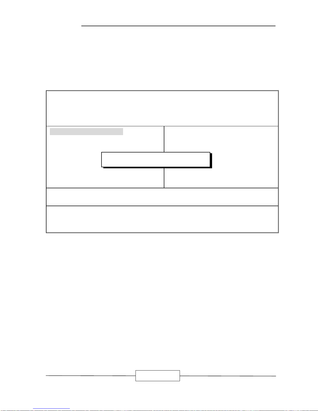
3.14 Save & Exit Setup
Selecting this option and pressing the <Enter> key to save the new setting information in
the CMOS memory and continue with the booting process.
The Screen appears as ...
ROM PCI / ISA BIOS (2A4KDL7F)
CMOS SETUP UTILITY
AWARD SOFTWARE, INC.
STANDARD CMOS SETUP
BIOS FEATURES SETUP
CHIPSET FEATURES SETUP
POWER MANAGEMENT SETUP
PCI CONFIGURATION SETUP
LOAD BIOS DEFAULTS
LOAD SETUP DEFAULTS
INTEGRATED PERIPHERALS
SUPERVISOR PASSWORD
USER PASSWORD
IDE HDD AUTO DETECTION
HDD LOW LEVEL FORMAT
SAVE & EXIT SETUP
EXIT WITHOUT SAVING
ESC : Quit á â à : Select Item
F10 : Save & Exit Setup (Shift) F2 : Change Color
Time, Date, Hard Disk Type...
Load SETUP Defaults (Y/N) ? Y
Page 49
BIOS SETUP
TF-486 / 43
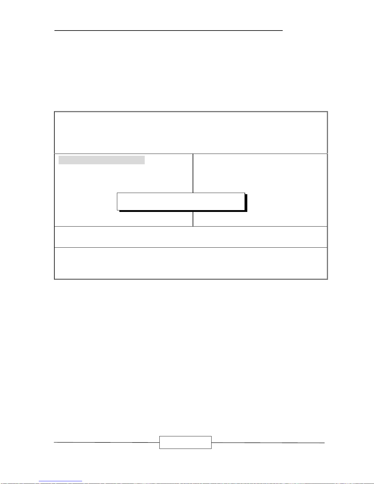
3.15 Exit Without Saving
Selecting this option and pressing the <Enter > key to exit the Setup Utility without
recording any new values or changing old ones.
The Screen appears as ...
ROM PCI / ISA BIOS (2A4KDL7F)
CMOS SETUP UTILITY
AWARD SOFTWARE, INC.
STANDARD CMOS SETUP
BIOS FEATURES SETUP
CHIPSET FEATURES SETUP
POWER MANAGEMENT SETUP
PCI CONFIGURATION SETUP
LOAD BIOS DEFAULTS
LOAD SETUP DEFAULTS
INTEGRATED PERIPHERALS
SUPERVISOR PASSWORD
USER PASSWORD
IDE HDD AUTO DETECTION
HDD LOW LEVEL FORMAT
SAVE & EXIT SETUP
EXIT WITHOUT SAVING
ESC : Quit á â à : Select Item
F10 : Save & Exit Setup (Shift) F2 : Change Color
Time, Date, Hard Disk Type...
Save to CMOS and EXIT (Y/N) ? Y
Page 50

TF-486 / 44
HOW TO USE WATCH-DOG TIMER
You could enable the watch-dog for when your application software monitors an
unexpected or not respond event, then the hardware timer generates a reset to reboot
your system. The watch-dog timer period (from enable to reset) was decided by the
jumper setting of the watch-dog time out period. Please refer the chapter of jumper
settings and connectors. During the period of enable to reset, you could still cancel
reset bt disabling the watch-dog.
EX.1: For DOS
Execute the DEBUG.EXE file under DOS, Then key-in i443. The system will reboot
automatically according to the time-out you set.
For example, if you want to Set 4 seconds for the time-out, you should set JP14: 4-8 ON
Enable
C:\DOS> DEBUG
-i443
Disable
C:\DOS>DEBUG
-i43
EX.2: For assemble Language
Enable :
:
:
MOV DX, 443H
IN AL, DX
:
:
Disable :
:
:
IN AL, 43H
:
:
APPENDIX A
Page 51
Terms and Conditions
Date:1999.07.05
Warranty Policy
1. All products are warranted against defects in materials and workmanship on a period
of one years from the date of purchase by the customer.
2. The buyer will bear the return freight charges for goods that are returned for repair
within the warranty period whereas manufacturer will bear the other way after repair.
3. The buyer will pay for repair (for the replaced materials plus service time) and
transportation charges (both ways) for items after the expiration of the warranty
period.
4. If the RMA Service Request Form does not meet the stated requirement as listed on
“RMA Service “ , RMA goods will be returned at the customer expense.
5. The following conditions are excluded from this warranty¡G
A. Improper or inadequate maintenance by the customer.
B. Unauthorized modification or misuse.
C. Operation outside of the environmental specifications for the product.
RMA Service
1. Request a RMA# :
Complete and fax to Supplier the “RMA Request Form” to obtain a RMA number.
2. Shipping:
A. The customer is requested to fill up the problem code as listed . If none of the
code is selected, please write the symptom description on the remark.
B. Ship the defective units with freight prepaid.
C. Mark the RMA # clearly on the box.
D. Shipping damage as a result of inadequate packing is the customer‘ s
responsibility.
E. Use the original packing materials whenever possible .
3. All RMA# are valid for 30 days only:
When RMA goods are received after valid RMA# period , the goods will be rejected.
Page 52
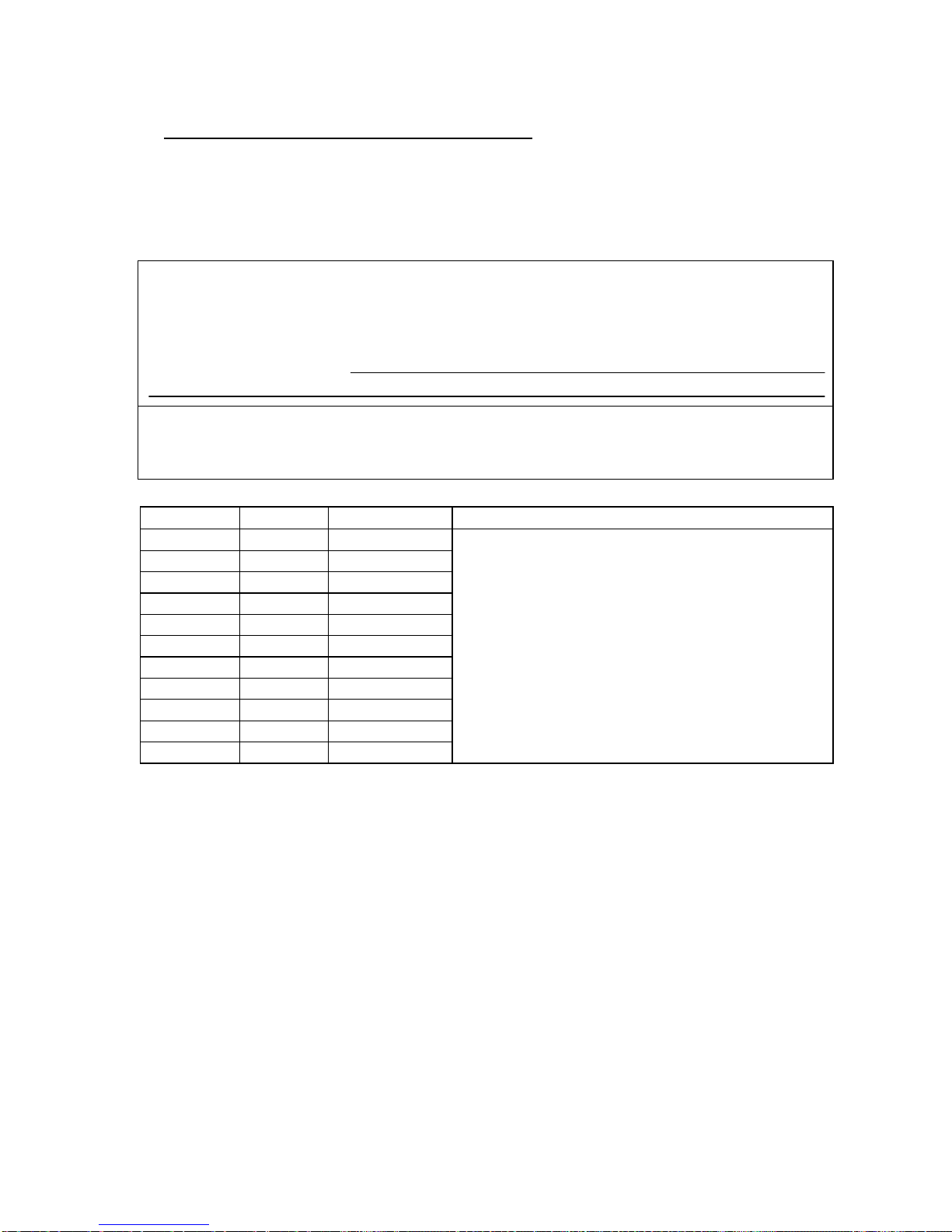
RMA Service Request Form
Date:1999.07.05
When requesting RMA service, please fill out this “RMA Service Request Form”.
This form needs to be shipped with your returns. Service cannot begin until we
have this information.
Company: Person to contact:
Phone No. Purchased Date:
Fax No.: Applied Date:
Return Shipping Address
*For Supplier only
RMA No:
Account Sales:
Model No. Serial No. Problem Code Remark
*This form could be copied for more description
*Problem Code:
01:D.O.A.
02: Second Time R.M.A.
03: No Screen
04: CMOS Data Lost
05: FDC Fail
06: HDC Fail
07: Bad Slot
08: BIOS Problem
09: Keyboard Controller Fail
10: Cache RMA Problem
11: Memory Socket Bad
12: Hang Up Hardware
13: Hang Up Software
14: Other ( Pls. Specify )
Request Party Confirmed By Supplier
Authorized Signatures Authorized Signatures
 Loading...