

Page 1

SERVICE MANUAL
21P8MDY5-A02
21T8MDY5-A01
I. Safety Instructions.........................................................................................................................2
II. Specifications..............................................................................................................................4
III. Level List of Equipments & Instruments Required for Production.................................................6
IV.Wiring Diagram...........................................................................................................................7
V. Block Diagram............................................................................................................................8
VI.Disassembly...............................................................................................................................9
VII. Input Signals & Equipments List for Alignment...........................................................................9
VIII. EEPROM Setting....................................................................................................................10
IX. Electrical Adjustment...............................................................................................................17
X. Transistor and IC Identification..................................................................................................18
XI. Schematic Diagram.................................................................................................................19
XII. Component Diagrams.............................................................................................................20
XIII. Exploded View Diagram.........................................................................................................24
This manual is the latest at the time of printing, and does not include the modification which
may be made after the printing, by the constant improvement of product.
Page 2
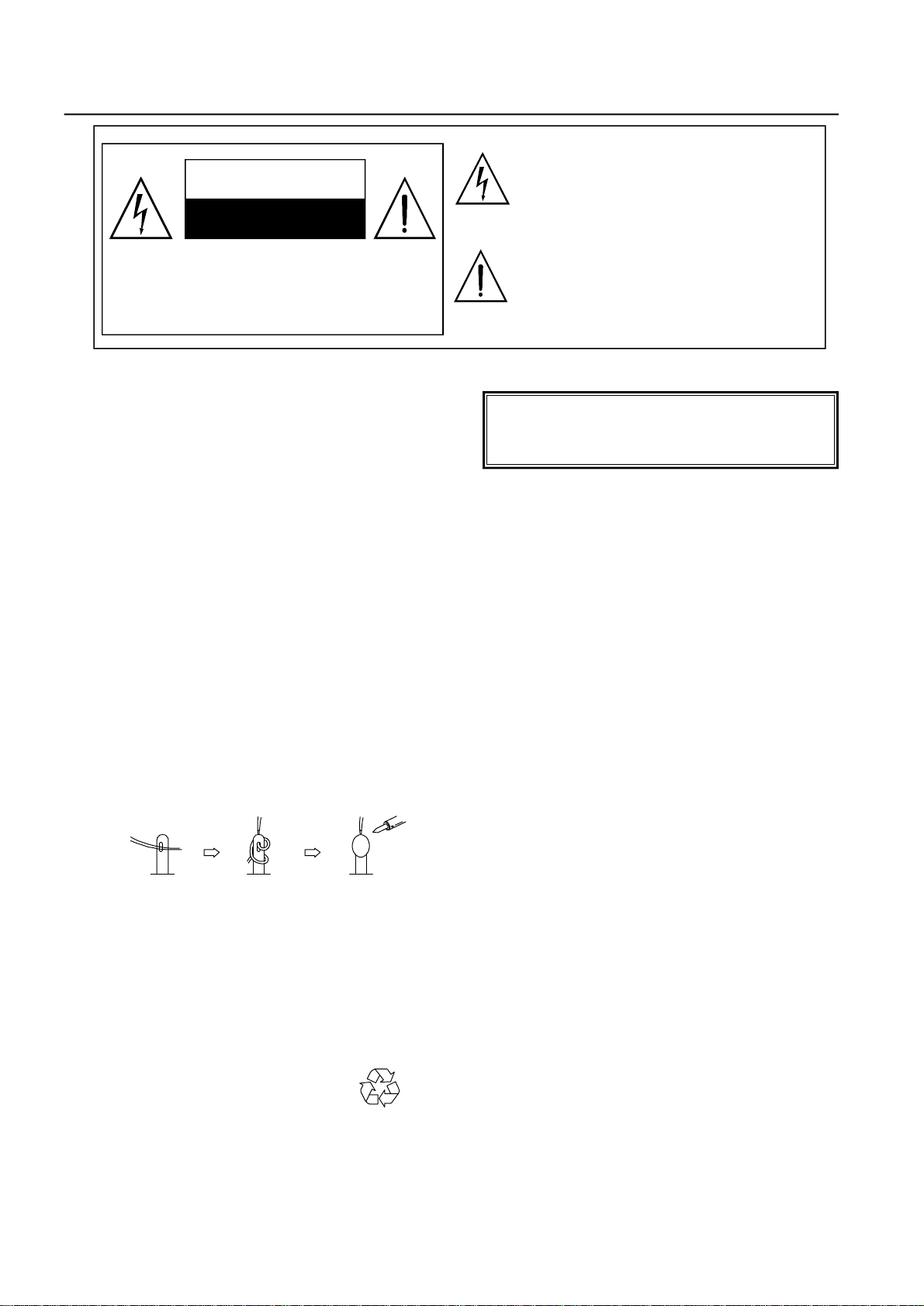
I. Safety Instructions
CAUTION
RISK OF ELECTRIC SHOCK
DO NOT OPEN
The lightning flash with arrowhead symbol,
within an equilateral triangle, is intended to alert
the user to the presence of uninsulated “dangerous
voltage” within the product’s enclosure that may
be of sufficient magnitude to constitute a risk of
electric shock to persons.
CAUTION: TO REDUCE THE RISK OF ELECTRIC
SHOCK, DO NOT REMOVE COVER (OR BACK). NO
USER-SERVICEABLE PARTS INSIDE. REFER
SERVICING TO QUALIFIED SERVICE PERSONNEL
ONLY.
PRECAUTIONS DURING SERVICING
1. In addition to safety, other parts and assemblies are
specified for conformance with such regulations as
those applying to spurious radiation. These must
also be replaced only with specified replacements.
Examples: RF converters, tuner units, antenna
selection switches, RF cables, noise-blocking
capacitors, noise-blocking filters, etc.
2. Use specified internal Wiring. Note especially:
1) Wires covered with PVC tubing
2) Double insulated wires
3) High voltage leads
3. Use specified insulating materials for hazardous
live parts. Note especially:
1) Insulating Tape
2) PVC tubing
3) Spacers (insulating barriers)
4) Insulating sheets for transistors
5) Plastic screws for fixing micro switches
4. When replacing AC primary side components
(transformers, power cords, noise blocking
capacitors, etc.), wrap ends of wires securely about
the terminals before soldering.
5. Make sure that wires do not contact heat generating
parts (heat sinks, oxide metal film resistors, fusible
resistors, etc.)
6. Check if replaced wires do not contact sharply edged
or pointed parts.
7. Make sure that foreign objects (screws, solder
droplets, etc.) do not remain inside the set.
MAKE YOUR CONTRIBUTION TO PROTECT THE
ENVIRONMENT
Used batteries with the ISO symbol
for recycling as well as small
accumulators (rechargeable batteries), mini-batteries
(cells) and starter batteries should not be thrown
into the garbage can.
Please leave them at an appropriate depot.
The exclamation point within an equilateral
triangle is intended to alert the user to the
presence of important operating and maintenance
(servicing) instructions in the literature
accompanying the appliance.
WARNING:
Before servicing this TV receiver, read the X-RAY
RADIATION PRECAUTION, SAFETY INSTRUCTION
and PRODUCT SAFETY NOTICE.
X-RAY RADIATION PRECAUTION
1. Excessively high can produce potentially hazardous
X-RAY RADIATION. To avoid such hazards, the high
voltage must not exceed the specified limit. The
normal value of the high voltage of this TV receiver
is 27 KV at zero bean current (minimum brightness).
The high voltage must not exceed 30 KV under any
circumstances. Each time when a receiver requires
servicing, the high voltage should be checked. The
reading of the high voltage is recommended to be
recorded as a part of the service record, It is
important to use an accurate and reliable high
voltage meter.
2. The only source of X-RAY RADIATION in this TV
receiver is the picture tube. For continued X-RAY
RADIATION protection, the replacement tube must be
exactly the same type as specified in the parts list.
3. Some parts in this TV receiver have special safety
related characteristics for X-RADIATION protection.
For continued safety, the parts replacement should
be under taken only after referring the PRODUCT
SAFETY NOTICE.
SAFETY INSTRUCTION
The service should not be attempted by anyone
unfamiliar with the necessary instructions on this TV
receiver. The following are the necessary instructions
to be observed before servicing.
1. An isolation transformer should be connected in the
power line between the receiver and the AC line
when a service is performed on the primary of the
converter transformer of the set.
2. Comply with all caution and safety related provided
on the back of the cabinet, inside the cabinet, on the
chassis or picture tube.
- 2 -
Page 3
3. To avoid a shock hazard, always discharge the
picture tube's anode to the chassis ground before
removing the anode cap.
4. Completely discharge the high potential voltage of the
picture tube before handling. The picture tube is a
vacuum and if broken, the glass will explode.
5. When replacing a MAIN PCB in the cabinet, always
be certain that all protective are installed properly
such as control knobs, adjustment covers or shields,
barriers, isolation resistor networks etc.
6. When servicing is required, observe the original lead
dressing. Extra precaution should be given to assure
correct lead dressing in the high voltage area.
7. Keep wires away from high voltage or high tempera
ture components.
8. Before returning the set to the customer, always
perform an AC leakage current check on the exposed
metallic parts of the cabinet, such as antennas,
terminals, screwheads, metal overlay, control shafts,
etc., to be sure the set is safe to operate without
danger of electrical shock. Plug the AC line cord
directly to the AC outlet (do not use a line isolation
transformer during this check). Use an AC voltmeter
having 5K ohms volt sensitivity or more in the
following manner.
Connect a 1.5K ohm 10 watt resistor paralleled by a
0.15µF AC type capacitor, between a good earth
ground (water pipe, conductor etc.,) and the exposed
metallic parts, one at a time.
Measure the AC voltage across the combination of
the 1.5K ohm resistor and 0.15 uF capacitor. Reverse
the AC plug at the AC outlet and repeat the AC
voltage measurements for each exposed metallic
part.
The measured voltage must not exceed 0.3V RMS.
This corresponds to 0.5mA AC. Any value exceeding
this limit constitutes a potential shock hazard and
must be corrected immediately.
The resistance measurement should be done
between accessible exposed metal parts and power
cord plug prongs with the power switch "ON". The
resistance should be more than 6M ohms.
PRODUCT SAFETY NOTICE
Many electrical and mechanical parts in this TV
receiver have special safety-related characteristics.
These characteristics are offer passed unnoticed by
visual spection and the protection afforded by them
cannot necessarily be obtained by using replacement
components rates for a higher voltage, wattage, etc.
The replacement parts which have these special
safety characteristics are identified by marks on
the schematic diagram and on the parts list.
Before replacing any of these components, read the
parts list in this manual carefully. The use of
substitute replacement parts which do not have the
same safety characteristics as specified in the parts
list may create shock, fire, X-RAY RADIATION or
other hazards.
Good earth ground
such as the water
pipe, conductor,
etc.
AC Leakage Current Check
AC VOLTMETER
Place this probe
on each exposed metallic
part
- 3 -
Page 4
II. Specifications
1. Power supply TV: AC 220-240V, 50/60Hz
Remote control battery: 3V (UM-4X2)
2. TV system RF input: PAL BG/DK/I, SECAM BG/DK, NTSC M /N
Video input: PAL/NTSC 3.58/NTSC 4.43/SECAM
3. Receiving channels 48.25MHz~588.25MHz
4. Intermediate frequencies Picture: 38.9MHz
5. Scanning Horizontal (Hz): 15625/15750
Vertical (Hz) : 50/60
6. Color picture tube : 21" 90 degree N(3) hemisphere Bv=0.5G(+0.1G/-0.15G)
7. Operating temperature Fulfil all specifications: 15°C ~ 35°C
Accept picture/tone reproduction: 5°C ~ 45°C
8. Operating relative humidity Fulfil all specifications: 45% ~ 75%
Accept picture/tone reproduction: 15% ~ 90%
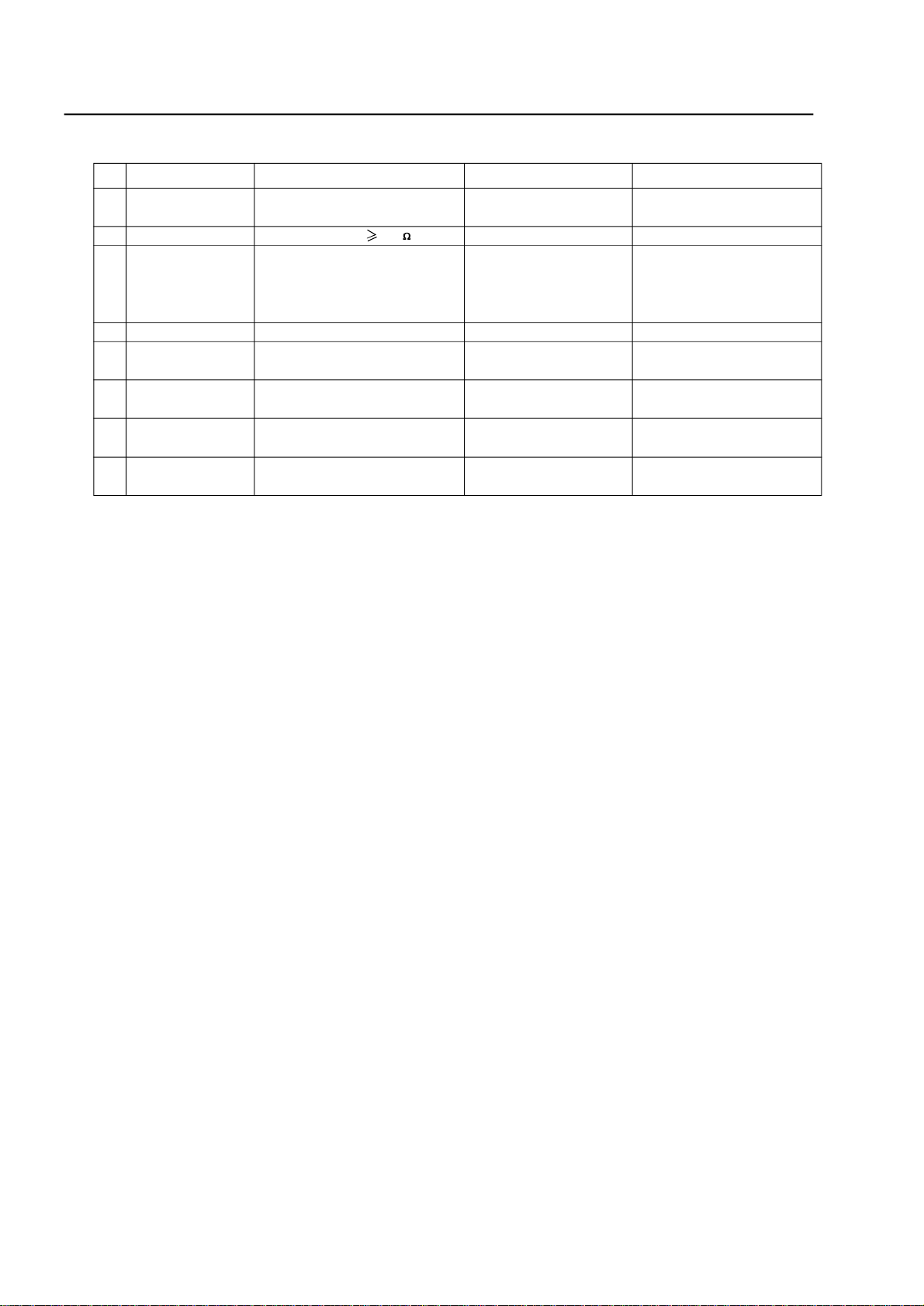
9. Electrical & Optical Specification:
No. Items Instruction Typical Limit Unit
1 Video sensitivity For 30dB S/N ≤45 ≤51 dBuV
2 FM sound sensitivity For 30dB S/N 30 ≤35 dBuV
3 Synchronizing sensitivity For RF transmission 30 ≤35 dBuV
4 Color sensitivity For RF transmission 32 ≤40 dBuV
5 Teletext sensitivity TV screen refreshes 40 times N/A N/A dBu
number of mistakes ≤8
6 Minimum NICAM threshold Without crackline noise N/A N/A dBu
7 AGC static characteristic Accept. Picture/tone repr. 103 ≥100 dBu
8 Selectivity Adjacent sound carrier 35 ≥30
Below adjacent sound carrier 35 ≥30 dB
Adjacent picture carrier 50 ≥40
Up adjacent picture carrier 45 ≥30
9 IF rejection 55 ≥50 dB
10 Image rejection VHF 55 ≥50 dB
UHF 50 ≥45
11 AFT pull-in range M/N ±1.0 ≥|±0.5| MHz
DK/I/BG +1.5 ≥|±1.0|
-1.0 ≥|±-0.75|
12 Chroma sync pull-in range ±500 ≥|±200| Hz
13 Color killer function -25 ≤-16 dB
14 DC restoration 3 ≤10 %
15 Resolution Horizontal PAL/SECAM 320 ≥300
NTSC 270 ≥250
Vertical PAL/SECAM 410 ≥400 lines
NTSC 320 ≥300
16 Overscan Cross hatch signal 93 91~97 %
17 Linearity Horizontal 7 ≤10 %
Vertical 6 ≤8 %
18 Pattern distortion 1.5 ≤3 %
19 Picture position In all direction ±3 ≤|±6| mm
20 Raster rotation In all direction 4 ≤6 mm
21 Convergence error 0.4 ≤0.6 %
22 White balance (8700°K) X 0.288 0.288±0.015
Y 0.298 0.298±0.015 /
23 Maximum full white At picture tube center 140 ≥100 cd/m
24 H sync pull-in range ±500 ≥|±200| Hz
25 V sync pull-in range 7 ≥6 Hz
26 Anode voltage 26.5 ≤27.5 KV
27 Audio frequence response ±3dB ref. to 1KHz 0.1~8.2 0.18~7.1 KHz
2
- 4 -
Page 5
No. Items Instruction Typical Limit Unit
28 Audio output power 1KHz 10% THD N/A N/A W
50KHz DEV. (BG/DK/I)
25KHz DEV. (M/N)
29 THD Po=0.5W 1KHz 1 ≤3 %
30 Signal to buzz ratio TV/AV 42 ≥40 dB
31 Minimum volume hum 6 ≤10 mVrms
32 Maximum woofer output power N/A N/A W
33 Woofer audio freqency response ±3dB ref. to 80Hz AV mode N/A N/A Hz
34 Bass control range 100Hz ref. to 1KHz AV mode N/A N/A dB
35 Treble control range 10KHz ref. to 1KHz AV mode N/A N/A dB
36 Balance Center 0 ≥|±2| dB
Max. 3 >2 dB
Min. -35 <−30 dB
37 Video input level 1.0 1±0.2 Vpp
38 Audio input level 0.5 0.5±0.3 Vrms
39 Video output level 1.0 1±0.2 Vpp
40 Audio output level 0.5 0.5±0.3 Vrms
41 Power consumpution Operating 75 ≤80 W
Stand by 6 ≤10 W
42 IR receiving distance ±30° 6 ≥4 m
43 X-ray radiation <0.1 ≤0.5 mR/h
44 Dielectric strength AC 3KVrms 1min. 3 ≤5 mArms
45 Y input level N/A N/A Vpp
46 Cr input level N/A N/A Vpp
47 Cb input level N/A N/A Vpp
48 White uniformity L edge or angle/L center 47 ≥45 %
49 Cross modulation Receiving Kawa central No visible interference at 80dBuv
interference system signals
50 The vibration noise from The distance between the No obvious vibration noise can be heard
electromagnetic devices in tester and the TV set is four
TV set times as many as the screen height
Test Condition
1 Picture Modulation 87.5%
2 Sound Modulation 27KHz Dev. For DK/I/BG
15KHz Dev. For M/N
3 Picture to Sound Ration 10dB
4 Sound Artificial Load Resistor 16 ohm
5 Video signal White and black
(three white & two black)
6 Audio signal 1KHz sine wave 0.5Vrms Convergence error test point on screen
7 Conditions of the TV setting:
A.Switch TV on and let it warm up for more than 30 minutes.
B.Connect RMS volt meter to speaker terminals and adjust theTV volume to get 500mW RMS power at each terminal.
C.Place the MINOLTA CA-100 test probe to white part of the screen,adjust the contrast until a reading of 80cd/m
D.Place the MINOLTA CA-100 test probe to black part of the screen,adjust the brightness until a reading of 2cd/m
E.Repeat step C & D until the exact luminance values is obtained or the nearest possible values you can get.then record the
luminance values & R.G.B gun voltage values at the same time. and take the largest values for measurement referenct.
F.Input standard color bar(100/0/75/0),then adjust the colour.until the waveforms at the blue gun of same level is obtained.
+P8 P5+
+P1
+P4 P2++P0
+P7 P6+
+P3
W
1/9H
1/9W
H
2
is obtained.
2
is obtained.
- 5 -
Page 6
III. Level List of Equipments & Instruments Required for Production
No. Designation Requirement Reference Model Remark
1 Pattern Generator System of output signal: PHILIPS
PAL DK/I., NTSC 3.58/4.43 PM5518-TN/ PM5418-TN
2 Digital voltmeter Input Resistance 10M FLUKE 45
3 Withstanding Withstanding Voltage:AC 1.5KV, KIKUSUI TOS 8650 For Irresistible Voltage
Voltage Tester 5KV/0-5KV±3% measurement
Cut-off current:AC 0-2mA,20mA/
Continuously Adjustable
4 Insulation Tester Test voltage:1000V. 500V KIKUSUI TOS 7100L
5 Oscilloscope Max Frequency of input signal:
20MHz or above
6 CRT Color MINOLTA CA-100 For White Balance
Analyzer Adjustment
7 Oscillator Frequency range of output KENWOOD AG-203A For generating Audio Signal
signal: 20Hz-20kHz
8 HV Probe FLUKE For screen voltage
adjustment
- 6 -
Page 7
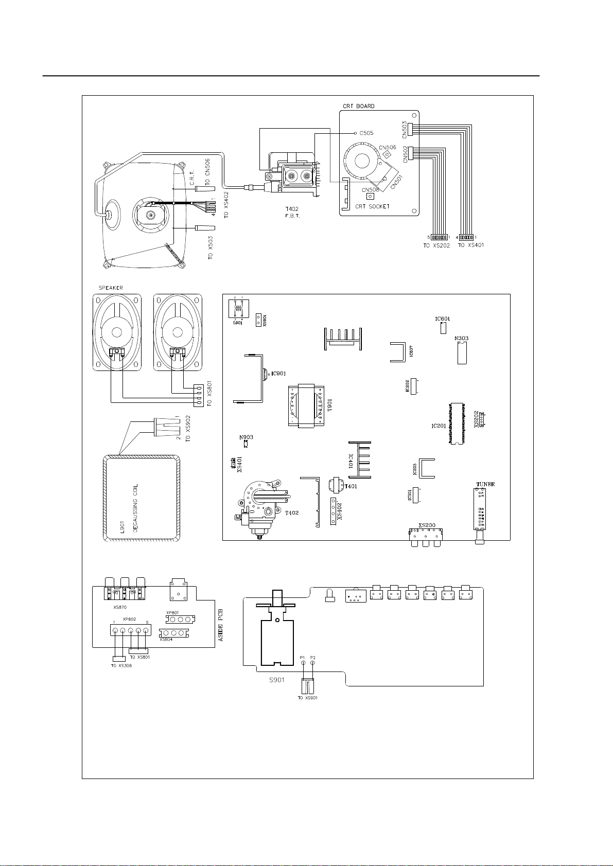
IV. Wiring Diagram
- 7 -
Page 8
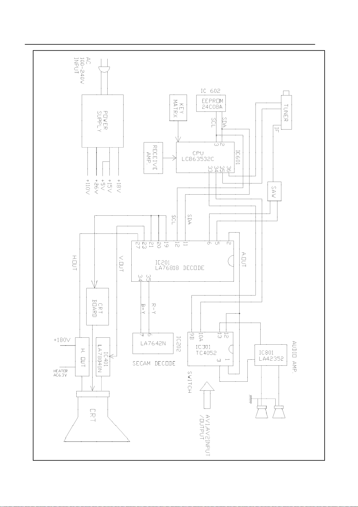
V. Block Diagram
- 8 -
Page 9

VI. Disassembly
In case of trouble, etc., necessitating disassemble, please disassemble in the order shown in the illustrations.
Reassemble in the reverse order.
1. Removal of the Back Cover
2. Removal of the MAIN PCB
a.Remove the screws.
b.Slide out the TV chassis slightly; pull up the connector of AC cord from PCB; pull up the CRT PCB from
CRT.
c. Remove the anode cap from the picture tube. To avaid a shock hazard, be sure to discharge the picture
tube’s anode to the chassis ground before removal.
d.Take out the TV chassis.
VII. Input Signals & Equipments List for Alignment
1. Equipments for adjustment
a. Pattern generator(PHILIPS PM 5518) b. Digital voltmeter
c. High voltage meter d. Demagnetiser
e. Personal computer (486) f. CRT colour analyzer (MINOLTA CA-100)
g. High voltage probe
2. Input signals
a. Color bar b.Cross hatch
c. Grey scale bar d. Monoscope pattern
e. Circle cross pattern
- 9 -
Page 10

VIII. EEPROM Setting
A. Factory debugging description
1. Enter/Exit factory debugging menu.
★ working keys
☆ Factory
* It can be enter to the factory menu directly.
* It can be turned over page after entering the factory debugging menu.
The content can be saved and exit the factory menu if pressing the key at the last pages of the factory
debugging menu.
☆ MENU
* Save the content and exit.
☆ ENTER WITH PASSWORD
* Press “2483” to enter the factory menu at “system menu” and “channel exchange” items.
2. Turn over pages of the factory debugging menu
★ working keys
☆ MUTE, FACTORY: turn over page backward
☆ CH.REV: turn over page forward
3. Change settings
★ working keys
☆ CH+/CH-: choose the items which going to be changed.
☆ VOL+/VOL-: to change the items which selected.
4. TV/AV switch
★ working keys
☆ TV/AV: press this button to switch the horizontal brightness line to adjust the G2 voltage.
B.Data Setting
Following data should be preset into the E2PROM IC before they are inserted to PCB.
P1
Name Adjust Range Advise value
*H.PHASE 0~31 13
*V.SIZE 0~127 52
*V.POS 0~63 27
*V.LIN 0~31 14
*V.SC 0~31 12
*NT.H.PHASE 0~7 6
*NT.V.SIZE 0~31 17
*NT.V.POS 0~31 25
*NT.V.LIN 0~7 4
1. Prss ‘ DISP ’ button to display the internal signal
2. When the “ + ” singal active
★ If select 50HZ of the item, the displaying frequence will force to 50HZ.
★ If select 60HZ of the item, the displaying frequence will force to 60HZ.
P2
Name Adjust Range Advise value
*R.B 0~255 100
*G.B 0~255 100
*B.B 0~255 100
*R.D 0~127 52
*G.D 0~15 12
*B.D 0~127 88
*S.B 0~127 63
V.K 0~1 0
1. While balance brightness line
★ Special working keys
☆ TV/AV button can turn on/off the white balance brightness line
2. Red, Green, Blue deflection voltage
★ Special working keys
☆ ‘1’/’4’: key can change the data of red deflection voltage.
☆ ‘2’/’5’: key can change the data of green deflection voltage.
☆ ‘3’/’6’: key can change the data of blue deflection voltage.
☆ ‘7’/’8’: key can change the data of accessory brightness.
- 10 -
Page 11

3. Auto while balance debugging
★ Enter to the debugging mode.
☆ Connect the MCU pin 25 to 0V under the factory menu.
★ After entering to the debugging mode, MCU will not control the IIC general line. Auto while balancecontrol program
can change the data of ‘ picture decode COMS chip ’ and ‘ 24C04/24C08’ freely.
★ About the while balance data’s relative address of the ‘ picture decode COMS chip ’ and 24C04/24C08.
Name Picture decode COMS Location 24C04/24C08 Location
chip address(HEX) address(HEX)
RED BIAS 07 7~0 1E 7~0
GREEN BIAS 08 7~0 1F 7~0
BLUE BIAS 09 7~0 20 7~0
RED DRIVE 0A 6~0 21 6~0
GREEN DRIVE 0B 3~0 22 3~0
BLUE DRIVE 0C 6~0 23 6~0
R-Y DC 1B 3~0 2C 3~0
B-Y DC 1B 7~4 2C 7~4
YUV R-Y DC 1B 3~0 2A 3~0
YUV B-Y DC 1B 7~4 2A 7~4
SECAM R-Y DC 1B 3~0 0D 5~2
SECAM B-Y DC 1B 7~4 09 6~3
P3
Name Adjust Range Advise value
SUB.CONT 0~31 10
SUB.COL 0~3 1
SUB.SHP 0~15 8
OSD.CONT 0~127 30
*OSD.POS 0~127 26
H.BLK.L 0~7 7
H.BLK.R 0~7 2
VIDEO.LVL 0~7 4
P4
Name Adjust Range Description Advise value
ENGLISH 0~1 ENGLISH OSD 1
0: NO; 1: YES
RUSSIAN 0~1 RUSSIAN OSD 1
0: NO; 1: YES
TURKISH 0~1 TURKISH OSD 0
0: NO; 1; YES
FRENCH 0~1 FRENCH OSD 0
0: NO; 1: YES
ARABIC 0~1 ARABIC OSD 1
0: NO; 1: YES
PERSIAN 0~1 PERSIAN OSD 0
0: NO; 1: YES
SPANISH 0~1 SPANISH OSD 0
0: NO; 1: YES
GERMAN 0~1 GERMAN OSD 0
0: NO; 1: YES
ITALIAN 0~1 ITALIAN OSD 0
0: NO; 1: YES
- 11 -
Page 12

P5
Name Adjust Range Description Advise value
VS/FS 0~1 0:Voltage synthesize high frequence cobbra 0
1:Frequence synthesize high frequence cobbra
VL/VH FREQ 0~255 Frequence: [(VL/VH FREQ.) + 100.25] MHZ 64
VH/UHF FREQ 0~255 Frequence: [(VH/UHF FREQ.) + 300.25] MHZ 164
AT.SCH.SIF 0~3 0: 6.5MHZ
1: 4.5MHZ 0
2: 5.5MHZ
3: 6.0MHZ
WOOFER 0~1 0: OFF 1: ON 0
INT.DVD 0~1 0: OFF 1: ON 0
DVD BLK. TIME 0~1 DVD and black screen time switch control 1
*VOL.CHANGE 0~1 0
*SEARCH SPEED 0~3 2
*Because of the port conflict, you can only select one between WOOFER and INT.DVD function, when one of it set to 1, another
will be set to 0 compulsively.
P6
Name Adjust Range Description Advise value
1-CHIP LA76818 Select decode IC LA76818
E2 CLEAR 0~1 1: Power on time, E2PROM data rewrite. 0
V-L 0~7 2
V-H 0~7 1
UHF 0~7 3
P.ON RESET 0~1 0: OFF mode 1
1: The mode before power off
H.TONE.MENU 0~1 1: Translucent user menu 1
V. MUTE.P.OFF 0~1 1: Turn off discharge 0
TEXT MENU 0~1 0: Picture menu title 1
1: teletext menu title
P7
Name Adjust Range Advise value
TV 0~1 1
AV1 0~1 1
AV2 0~1 1
DVD 0~1 0
TV.VLT 0~3 0
AV1.VLT 0~3 1
AV2.VLT 0~3 2
DVD.VLT 0~3 3
*INT.DVD.CH 0~2 0
P8
Name Adjust Range Advise value
ST.BRI 0~15 9
ST.CONT 0~15 9
ST.COL 0~15 7
ST.SHP 0~15 7
L.BRI 0~15 10
L.CONT 0~15 11
L.COL 0~15 9
L.SHP 0~15 7
- 12 -
Page 13

P9
Name Adjust Range Advise value
V.BRI 0~15 10
V.CONT 0~15 13
V.COL 0~15 11
V.SHP 0~15 7
SO.BRI 0~15 5
SO.CONT 0~15 7
SO.COL 0~15 5
SO.SHP 0~15 1
* P8, P9 for debugging each preparing value of four special picture mode, you can press P.P button directly at this two
pages toswitch different picture mode and observe the effect.
P10
Name Adjust Range Description Advise value
VIF.SYS 0~3 0=38.0MHZ 1
1=38.9MHZ
2=45.75MHZ
3=39.5MHZ
PAL 0~1 0:NO PAL COLOR DEMODULATION 1
1:PAL COLOR DEMODULATION
N3.58 0~1 0: NO NTSC3.58 COLOR DEMODULATION 1
1:NTSC3.58 COLOR DEMODULATION
N4.43 0~1 0: NO NTSC4.43 COLOR DEMODULATION 1
1:NTSC4.43 COLOR DEMODULATION
SECAM 0~1 0: NO SECAM COLOR DEMODULATION 1
1: SECAM COLOR DEMODULATION
DK 0~1 0:NO 6.5M SOUND DEMODULATION 1
1: 6.5M SOUND DEMODULATION
BG 0~1 0: NO 5.5M SOUND DEMODULATION 1
1: 5.5M SOUND DEMODULATION
I 0~1 0: NO 6.0M SOUND DEMODULATION 1
1: 6.0M SOUND DEMODULATION
MN 0~1 0: NO 4.5M SOUND DEMODULATION 1
1: 4.5M SOUND DEMODULATION
P11
Name Adjust Range Description Advise value
BG 0~3 No singal background
0: bule 0
1: black
2: red
3: yellow
BG.BRI 0~15 No singal background brightness 8
LOGO 0~1 0: No logo 1
1: personal logo
M.SCR.POS 0~31 openning center adjustment 0
M.SCR.TIME 0~3 0: 4s 2: 6s 1
1: 5s 3: 7s
TV ON EFF 0~2 0: Black screen > turn on
1: Black screen> opening>turn on 1
2: Black screen> logo> turn on
TV. OFF.SCR 0~1 TV OFF SCREEN 1
0:No TV off screen; 1:TV off screen
* When the cursor mark stay at item ‘BG’, ‘BG.BRI’, the ‘no singal backgroud’ effect which you have selected would
open automatically, the ‘ no singal backgroud brightness’ will also active at the same time.
- 13 -
Page 14

P12
Name Adjust Range Advise value
BY 0~15 8
RY 0~15 9
YUV.BY 0~15 8
YUV.RY 0~15 8
SCM.BY 0~15 5
SCM.RY 0~15 6
P13
Name Adjust Range Description Advise value
PWM. VOL 0~1 PWM volume control
0: no PWM volume control 1
1: pin 29,30 PWM volume control
PWM.2CH 0~1 0: pin29, 30 PWM volume can not 0
control single.
1: pin29, 30 PWM volume can control
single
1- CHIP VOL 0~127 PWM volume control, bring to front 127
and zoom in output control
RF.AGC 0~31 loudspeaker AGC 24
AV.OUT.OPT 0~1 AV output singal selection
0: AV output watching picture 0
1: AV output the TV signal
CH.OSD.BLACK 0~1 1: Channel exchange OSD black 1
screen
CH. TURN.MUTE 0~1 0: No black screen 1
1: Black screen
A.PMUTE 0~1 MCU 24pin exchange channel mute
0: Mute ; 1: No mute 0
P14
Name Adjust Range Description Advise value
AFC.G.G 0~1 AFC Stronger 0
VSEPUP 0~1 0: Normal; 1: Stronger 0
CD. MODE 0~7 3
DIGITAL. OSD 0~1 0: simulate; 1: Digital 0
V.OFFSET 0~3 0: min.; 3: max. 3
FM.LVL 0~31 31
P15
Name Adjust Range Description Advise value
BRT.ABL.DEF 0~1 0: ON; 1: OFF 0
MID.STP.DEF 0~1 0: ON; 1: OFF 0
BRT.ABL.TH 0~5 3
RB. GAIN.BAL 0~15 8
RB.ANG 0~15 8
AT. FLESH 0~1 0
VOL. FIL 0~1 0
- 14 -
Page 15

-Factory debugging menu 818/828 P1
Name Adjust Range Description Advise value
V.R.TIME 0~1 0: Normal; 1:0.25 horizontal windage 0
A.M.SW 0~1 0: Normal; 1: External sound 1
WPL 0~3 0
Y.APF 0~1 1
Y.GAM.ST 0~3 0
VCO.SW 0~1 0: debugging backward; 0
1: debugging forward
VCO.ADJ 0~3 0: 0HZ
1: 30HZ 2
2: 60HZ
3: 90HZ
PAL.COL.SW 0~1 1
PAL.COL 0~15 7
-Factory debugging menu 818/828 P2
Name Adjust Range Description Advise value
H.TONE 0~3 0: Darkness; 3: lightness 3
GRAY. MODE 0~1 0:100% White singal 0
1: 60% White singal
CROSS 0~3 Internal singal
0: undisplay the internal signal 0
1: Black singal
2: While singal
3: Cross singal
GY.ANG 0~1 0: 240 angle; 1:253 angle 1
C.KILL.OPE 0~7 0: -30dB
7: -40Db 7
-Factory debugging menu 818/828 P3
Name Adjust Range Description Advise value
VBLK.SW 0~1 0: Normal; 1: stronger 0
FBPBLK.SW 0~1 0: LA76818 control 1
1: Internal/External control
P/O.SW 0~3 0: Debugging forward 1
1: Debugging backward
P/O.SHOOT 0~1 Signal forward and backward debugging 3
DC.REST 0~3 0: 100%
1: 107% 0
2: 113%
3:129%
BLK.STR.ST 0~3 0: black electricity extend=OFF
1:black electricity extend=ON(40IRE)
2:black electricity extend=ON(60IRE) 1
3: black electricity extend=OFF
BLK.STR.GN 0~3 0: Min.; 2: Max. 2
RGB.TEMP.SW 0~1 0: -1VBE
1: Normal 0
CORING.GN 0~3 0: Min. ; 3: Max. 2
* When the cursor mark stay at ‘ BLK.STR.ST’, ‘BLK.STR.GN’ , the customer ‘ picture stronger’ function will open automatically in
order to adjust the function effect expediently.
* when the cursor mark stay at ‘ CORING.GN’ , the custormer’ decrease noise’ function will open automatically in
order to adjust the function effect expediently.
- 15 -
Page 16

- Input the LOGO: “ERISSON”
★ This page will not appear unless the E2PROM set to 24C08
★ working key:
☆ ‘0’ / ‘1’: LOGO up/move down
☆ ‘2’ / ‘3’: LOGO left/move right
☆ ‘4’: to change the LOGO color
☆ ‘5’: to change the LOGO size
☆ ‘6’: to switch the rows of the LOGO
☆ ‘7’: reset
★ MENU: save and exit
★ CH+ / CH-: to change the letter position which need to be changed.
★ VOL+ / VOL-: to change the letter
★ aging debugging page
★ The TV will not Off automatically without signal
The chassis address which require from the white balance debugging as below:
LA76818 Sub Address AT24C08 Sub Address
Device Address BAH A0H Bit Map
Red Bias 07H 16H+08H=1EH 0FFH
Green Bias 08H 17H+08H=1FH 0FFH
Blue Bias 09H 18H+08H=20H 0FFH
Red Drive 0AH 19H+08H=21H 07FH
Green Drive 0BH 1AH+08H=22H 00FH
Blue Drive 0CH 1BH+08H=23H 07FH
Sub Bright 0DH 1CH+08H=24H 07FH
“ * ” means that the data can be changed during the production or debugging.
- 16 -
Page 17

IX. Electrical Adjustment
A. +B Voltage Alignment
a. Preparation Procedure
1).Receive standard colour bar signal.
2).Press key "P.MODE." to select “STANDARD” mode.
3).Connect digital voltmeter between of C917 and GND.
4).Adjustment Step
Adjust RP901 to make the read-out on the Voltmeter to be as follows:
MODEL CRT CRT TYPE NO +B
21P8/T8MDY5 E6120-027006 A51MAT70X5S(C) N3 SEG 110V
B. Adjustment for AFC
a.Preparation procedure
1.Turn on the main power switch.
2.Set digital voltmeter at DC, then connect it’s probe across of IC201 PIN47 and GND.
3.
a. To set the pattern generator under the color bar and pal system. Apply 100dBµV 38.9 MHz
IF signal between IF input pin and GND of the TUNER on main PCB board
21P8/T8MDY5
b. (see Fig.1).
C212
(Fig.1)
IF
C101
b. Adjust the IFT coil T202 until the meter indicates 3.6V±0.05V.
DIGITAL VOLTMETER
Output
Pattern
Generator
- 17 -
Page 18

X. Transistor and IC Identification
A. Main Unit:
- 18 -
Page 19

XI. Schematic Diagram
i.(Please refer to A315-004.pdf)
- 19 -
Page 20

XII. Component Diagrams
i. Main & CRT PCB component diagram (Top/Bottom view)
(Please refer to E3701-054080A/B pdf)
- 20 -
Page 21

ii. CRT ERISSON PCB component diagram (Top/Bottom view)
(Please refer to E3701-021080-10 pdf)
- 21 -
Page 22

iii. KEY&POWER&ASIDE PCB component diagram (Top/Bottom view)
(For 21P8MDY5 model)
(Please refer to E3701-054100A/B/C .pdf)
iii. KEY&POWER&ASIDE PCB component diagram (Top/Bottom view)
(For 21T8MDY5 model)
(Please refer to E3701-054130A/B/C .pdf)
- 22 -
Page 23

XIII. Exploded View Diagram
Main Unit
i. For 21P8MDY6-A02 model
Item Part No. Description Qty.
1 200-21P801-XXR Cabinet Front 1
2 612-300310-10 S-TAP.Scerw Flt 3x10 3
3 279-21P801-XXS Power Knob 1
4 E3701-022070C LED PCB 1
5 E3701-022070A Power PCB 1
6 615-400214-10 Screw 4x14 2
7 254-871401-01R CLP CRD PER 8714 1
8 376-391501-01Y Pubber Ring (T=3.0mm) 4
9 21” Colour CRT 1
10 639-382802-01 Special WasherCRT 4
11 614-500430-10 S-TAP. Screw Bid 4x30 4
12 249-922002-01F Special Plastic Part 2
13 E3701-XXXXXX CRT PCB 1
14 202-21T80X-0XX Back Cabinet Black HI-PS 1
15 614-500425-00 S-TAP. Screw B/T 5x25mm Black 6
Item Part No. Description Qty.
16 387-21T801-XXH Model Plate 1
17 614-400414-10 S-TAP. Screw B/T 4x14mm White 1
18 389-21B8XX-0XH RCA Plate 1
19 611-300310-00 S-TAP. Screw Flt 3x10 2
20 389-21T80X-XXH RCA Cover Plate 1
21 477-371601-01 Spring + CRT 1
22 E3701-XXXXXX Main PCB Ass’y 1
23 E3701-022070B AV PCB Ass’y 1
24 615-400414-10 S-TAP. Screw Bwh 4x14 8
25 379-972501-01Y Special Rubber Parts 8
26 379-972502-01Y Special Rubber Parts 8
27 E4801-XXXXXX Speaker 2
28 486- Name Plate 1
29 269-25P801-01L Sensor Lens 1
30 277-21P801-XXS Func Keys 1
- 23 -
Page 24

ii. For 21T9MDY5-A01 model
Item Part No. Description Qty.
1 200-21T801-XXR Cabinet Front 1
2 612-300310-10 S-TAP.Scerw Flt 3x10 3
3 279-21T801-XXS Power Knob 1
4 E3701-022060C LED PCB 1
5 E3701-022060A Power PCB 1
6 615-400214-10 Screw 4x14 2
7 254-871401-01R CLP CRD PER 8714 1
8 376-391501-01Y Pubber Ring (T=3.0mm) 4
9 E6101-XXXXXX21” Pure Flat CRT or Nomal Flat CRT 1
10 639-382802-01 Special WasherCRT 4
11 614-500430-10 S-TAP. Screw Bid 4x30 4
12 249-922002-01F Special Plastic Part 2
13 E3701-XXXXXXCRT PCB 1
14 202-21T80X-0XX Back Cabinet Black HI-PS 1
15 614-500425-00 S-TAP. Screw B/T 5x25mm Black 6
Item Part No. Description Qty.
16 387-21T801-XXH Model Plate 1
17 614-400414-10 S-TAP. Screw B/T 4x14mm White 1
18 389-21B8XX-0XH RCA Plate 1
19 611-300310-00S-TAP. Screw Flt 3x10 2
20 389-21T80X-XXH RCA Cover Plate 1
21 477-371601-01 Spring + CRT 1
22 E3701-XXXXXXMain PCB Ass’y 1
23 E3701-022060B AV PCB Ass’y 1
24 615-400414-10 S-TAP. Screw Bwh 4x14 8
25 379-972501-01Y Special Rubber Parts 8
26 379-972502-01Y Special Rubber Parts 8
27 E4801-XXXXXXSpeaker 2
28 486- Name Plate 1
29 277-21P801-XXS Func Keys 1
30 269-210801-01L Sensor Lens 1
- 24 -
 Loading...