

Page 1
LC D-T V Ser vic e Man ual
15”19”22” LCD COLOR TV
15”19”22” LCD COLOR TV
Service Manual
Service Manual
MODEL NO.:
L15372E2800/15LJ18
L19372E2800/19LJ08
L22372E2801/22LDJ08
Page 2

LC D-T V Ser vic e Man ual
Contents
Safety Notice … ………………………………………………………………......03
Supported Operating Modes ………………………………………………..…...04
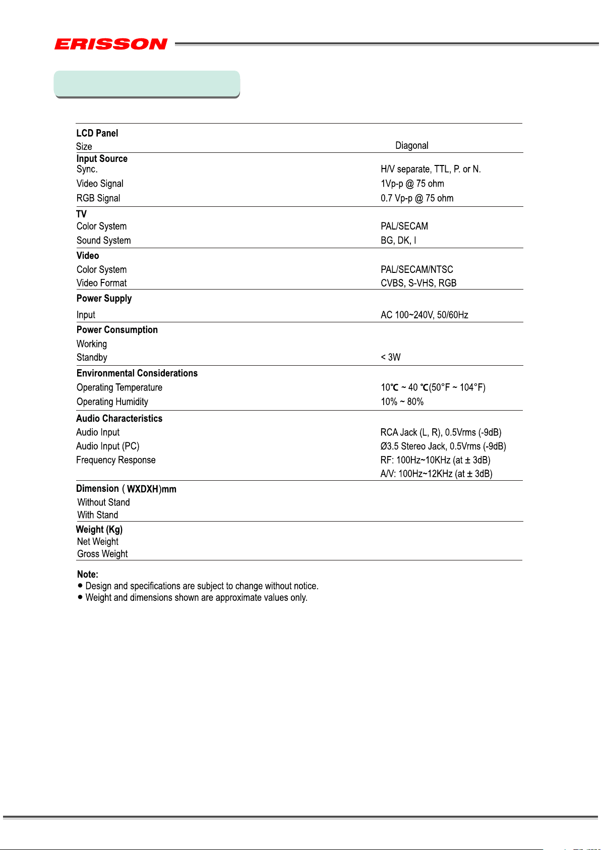
Specifications …………………………………………………………………..…06
Location and Function of Controls...........................................................09
Disassembly the Framework ……………………………………………….……12
Illustration of actual object ………………………………………….……………18
.
Driver PCB Principle Diagram ………………………………………….…..…...26
DVD PCB Principle Diagram ………………………………………….…..….....35
Power PCB Circuit Diagram…………………………………………….…………36
Block Diagram......................................................................................40
Trouble Shooting Charts ……...…………………………………...……………43
(02)
Page 3
LC D-T V Ser vic e Man ual
Safety Notice
Warning
Be sure to read this manual before servicing .To assure safety from fire ,electric
shock ,injury ,harmful radiation and
materials, various measures are provided in this liquid crystal television/monitor.
Be sure to read the cautionary items described in the manual to maintain safety
before servicing.
TO REDUCE THE RISK OF
CA UT ION
RISK OF ELECTRIC
SHOCK DO NOT
OPEN
This symbol indicates
“dangerous voltage”
inside the product that
presents a risk of electric
shock or personal injury.
ELECTRIC SHOCK DO NOT
REMOVE COVER.NO
USER-SERVICEABLE
PARTS INSIDE. REFER
SERVICING TO QUALIFIED
SERVICE PERSONNEL.
This symbol indicates
important instructions
accompanying the
product.
Service Warning
.The LCD Panel Module is made of glass. When handling broken LCD Panel
Module ,take special care not to be injured.
.Replacement work should only start after the LCD Panel Module and the AC/DC
Power Supply has become sufficiently cool.
.Take special care of the LCD display panel and do not damage its surface.
.Do not touch the LCD Panel Module with your bare hands and protect its surface
from stains.
.It is recommended to use clean soft gloves during servicing in order to protect
the LCD display panel and the
(03)
Page 4
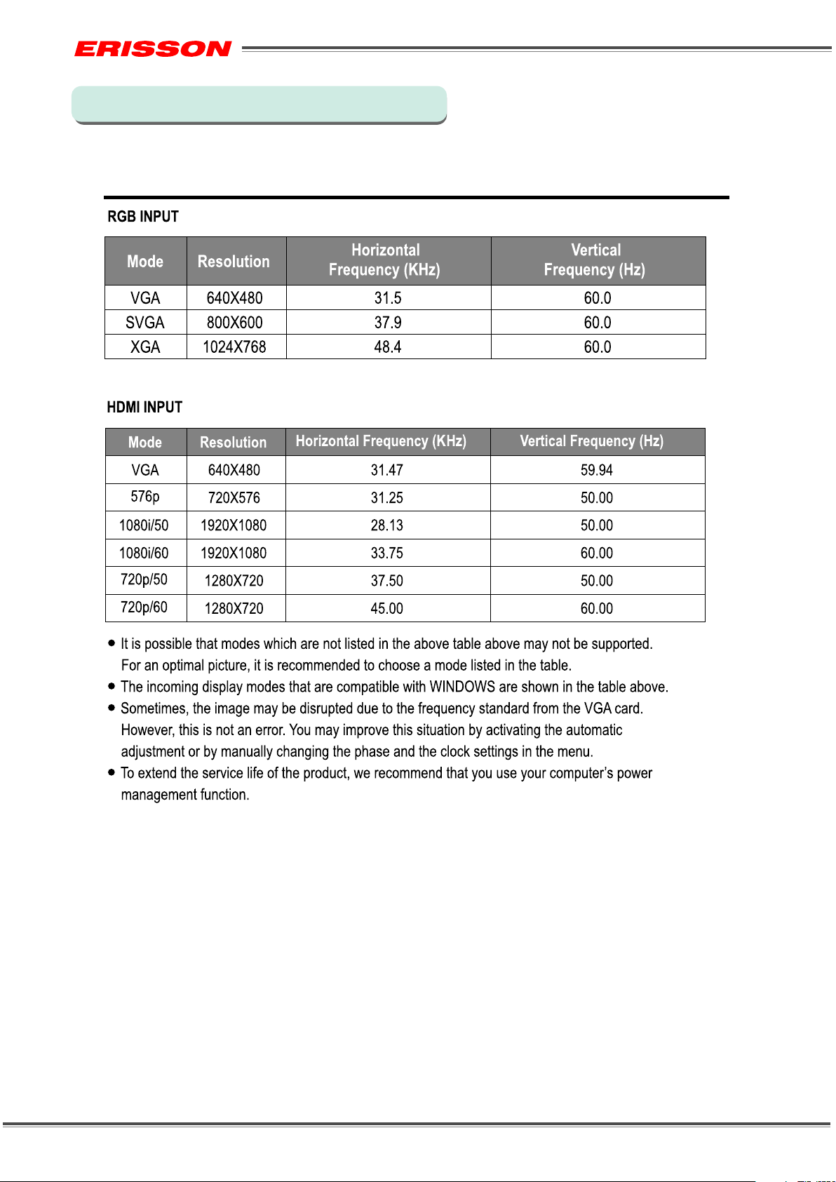
Supported Operating Modes(1)
L15372E2800/15LJ18
LC D-T V Ser vic e Man ual
(04)
Page 5
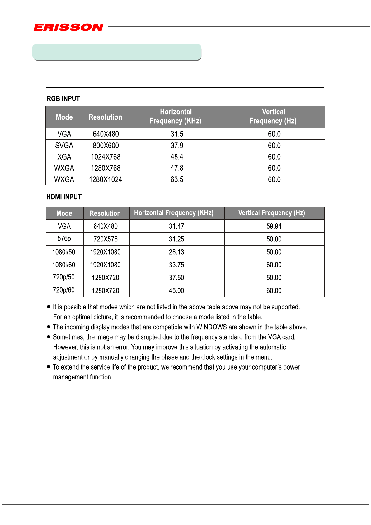
Supported Operating Modes(2)
L19372E2800/19LJ08
L22372E2801/22LDJ08
LC D-T V Ser vic e Man ual
(04)
Page 6
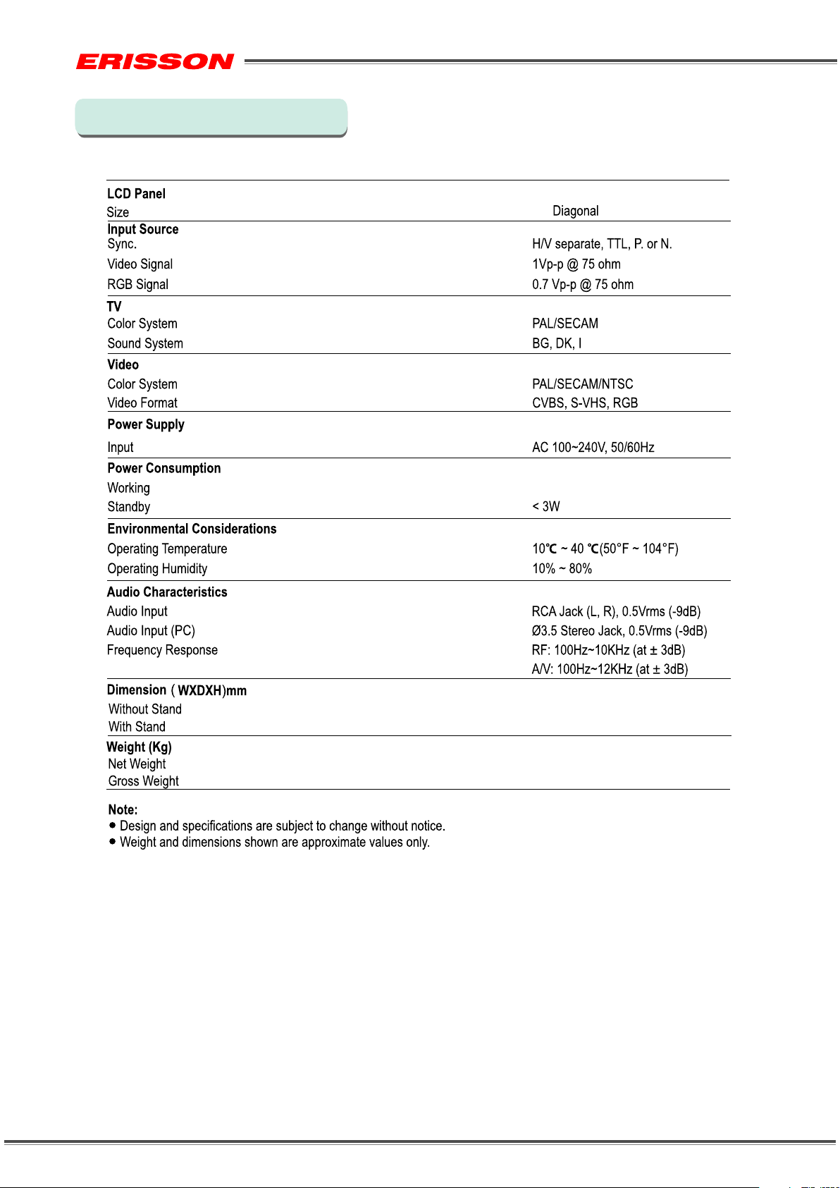
Specifications(1)
L15372E2800/15LJ18
LC D-T V Ser vic e Man ual
15’’
45W
380 X70X315
380 X135X364
2.7
3.8
(06)
Page 7
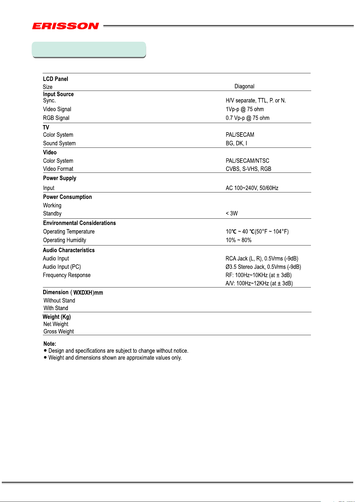
Specifications(2)
L19372E2800/19LJ08
LC D-T V Ser vic e Man ual
19’’
60W
480 X84X360
480 X175X392
4.6
5.7
(07)
Page 8
Specifications(3)
L22372E2801/22LDJ08
LC D-T V Ser vic e Man ual
22’’
70W
550X82X411
550X175X443
5.5
7
(08)
Page 9
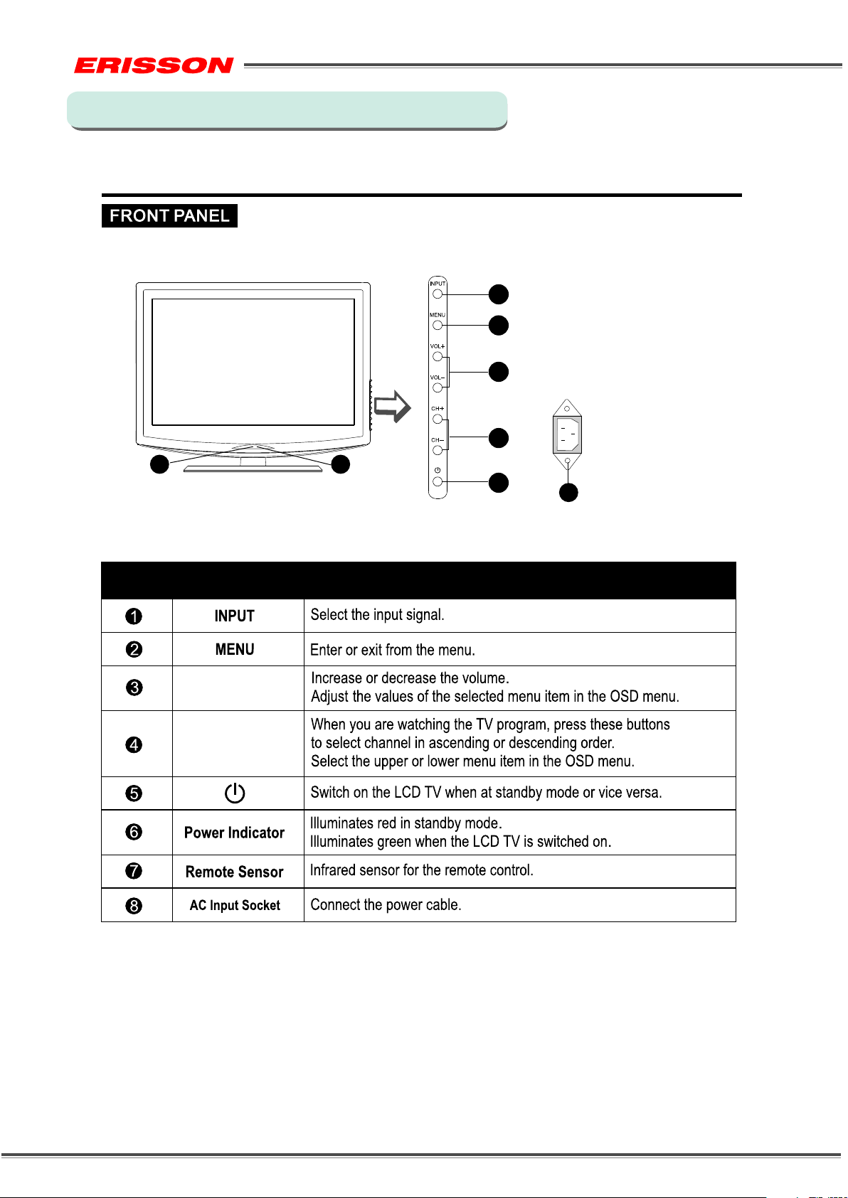
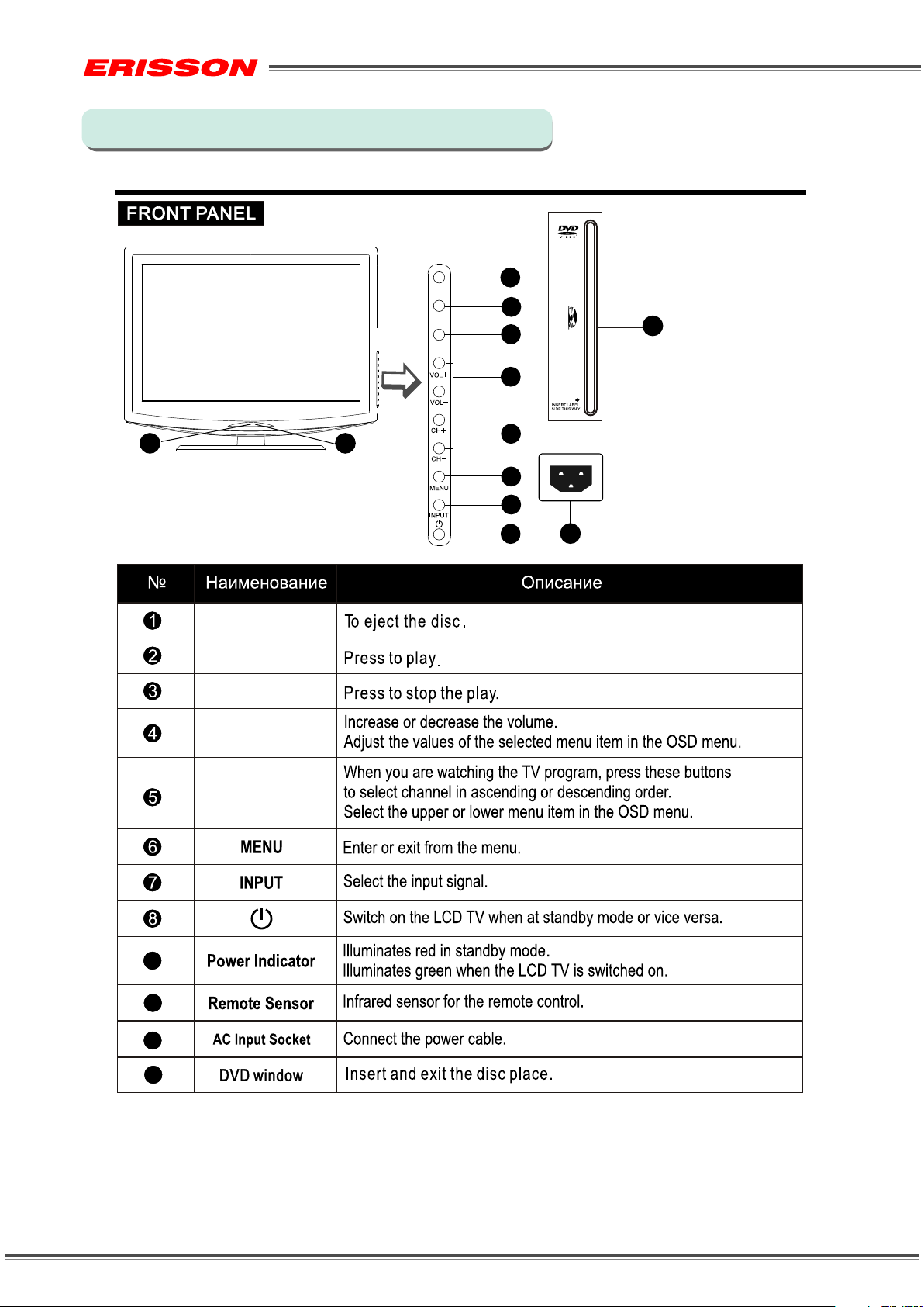
Location and Function of Controls(1)
L15372E2800/15LJ18
L19372E2800/19LJ08
LC D-T V Ser vic e Man ual
11
22
33
44
NO.
66
Button Name
VOL+/-
CH+/-
77
55
Description
88
Note:
If there is no signal input for 5 minutes, the LCD TV will switch to standby automatically. The power
indicator will light up in red.
(09)
Page 10
Location and Function of Controls(2)
L22372E2801/22LDJ08
LC D-T V Ser vic e Man ual
OPE N
PLAY
STOP
11
22
33
1212
44
99
1010
55
66
77
88
OPEN
PLAY
STOP
1111
VOL+/-
CH+/-
9
10
11
12
Note:
If there is no signal input for 5 minutes, the LCD TV will switch to standby automatically. The power
indicator will light up in red.
(10)
Page 11
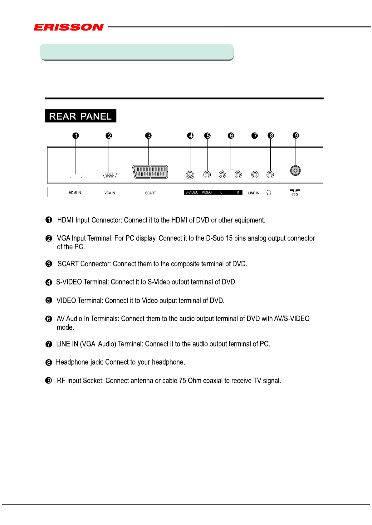
Location and Function of Controls(3)
L15372E2800/15LJ18
L19372E2800/19LJ08
L22372E2801/22LDJ08
LC D-T V Ser vic e Man ual
(11)
Page 12
LC D-T V Ser vic e Man ual
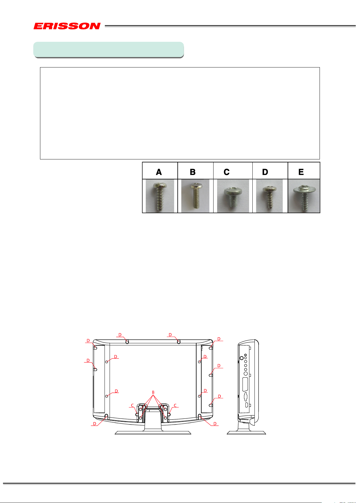
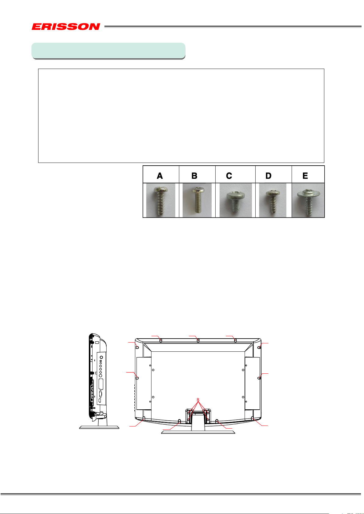
Disassembly the Framework(1)
Please follow the following stops to disassemble the unit :
Warning:
All material parts and screws must be installed on its corresponding position
correctly ,otherwise it may cause damage.
All the connection cable must be disconnected otherwise it may cause damage.
Warning :
Disassemble the unit only should be handled by qualified service personnel !
Assembly and disassembly must be noted to protect cabinet to avoid scratch
and damage.
L15372E2800/15LJ18
1、 Disassemble the rear cabinet:
1.1、Unfasten the 4 screws B(BM4×10 ), take out the stand from the TV;
1.2、Unfasten the 9 screws D( BST3×10),2screws C(BM3X6), and the 4
screws D(BST3X6 ), uninstalling the back cover .
Warning:
When remove the stand bracket, please be careful of the LCD panel should
not be contacted any edge and firm or corrosive object, they may case
scratch and damage.
(12)
Page 13
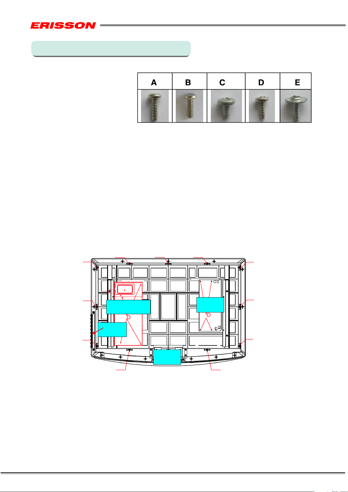
Disassembly the Framework(1-1)
L15372E2800/15LJ18
2、Disassemble PCB assembly and rear cabinet:
2.1、Uninstall the Connection cable with Drive PCB1、Power PCB2、
Key PCB3、Remote PCB4 ;
2.2、Unfasten 4 Screws of D(BST3×10 ), and take out the Drive PCB1;
2.3、Unfasten 4 screws of D(BST3×10 ) ,and take out the Power PCB2;
2.4、Unfasten 4 screws of D(BST3×10 ) ,and take out the LCD Panel.;
LC D-T V Ser vic e Man ual
Drive PCB(1)
key
PCB(3)
Remote
PCB(4)
Power
PCB(2)
LCD Panel
(02)
Warning:When Disassemble the Drive PCB and Power PCB ,
please be careful of avoiding the connector pins to be flexed.
(01)
(13)
Page 14
LC D-T V Ser vic e Man ual
Disassembly the Framework(2)
Please follow the following stops to disassemble the unit :
Warning:
All material parts and screws must be installed on its corresponding position
correctly ,otherwise it may cause damage.
All the connection cable must be disconnected otherwise it may cause damage.
Warning :
Disassemble the unit only should be handled by qualified service personnel !
Assembly and disassembly must be noted to protect cabinet to avoid scratch
and damage.
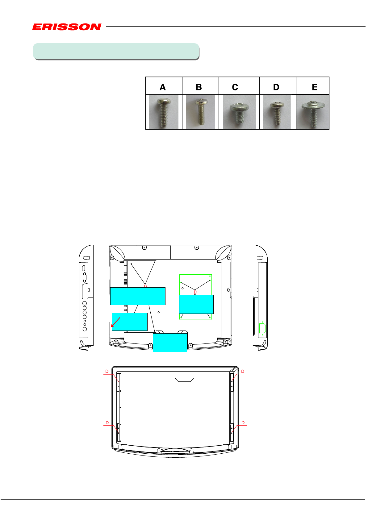
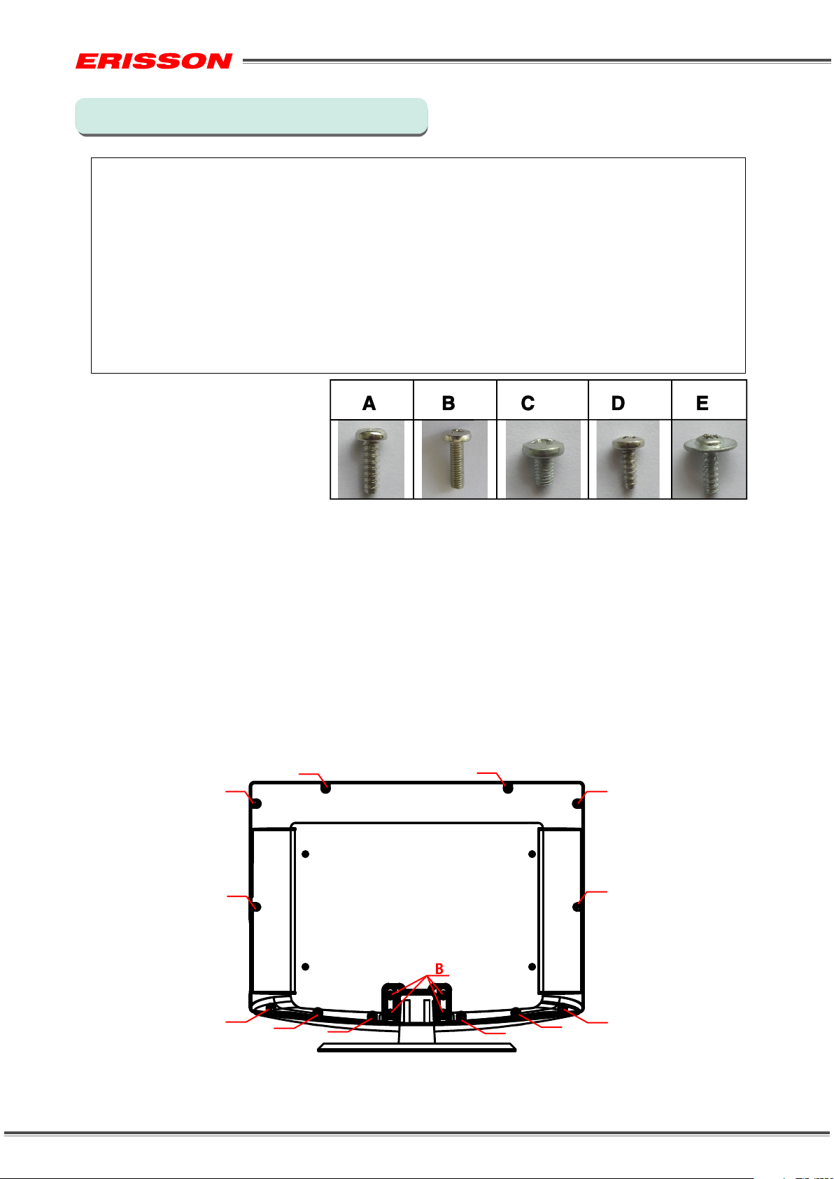
L19372E2800/19LJ08
1、 Disassemble the rear cabinet:
1.1、Unfasten the 4 screws B(BM4×12 ), take out the stand from the TV;
1.2、 11
uninstalling the back cover .
Warning:
When remove the stand bracket, please be careful of the LCD panel should
not be contacted any edge and firm or corrosive object, they may case
scratch and damage.
Unfasten the screws D( BST3×10), and the 4 screws D(BST3X8 ),
D
D
D
D
D
D D
D
D
D
D
D
D
D
D
(14)
Page 15
LC D-T V Ser vic e Man ual
Disassembly the Framework(2-1)
L19372E2800/19LJ08
2、Disassemble PCB assembly and rear cabinet:
2.1、Uninstall the Connection cable with Drive PCB1、Power PCB2、
Key PCB3、Remote PCB4;
2.2、Unfasten 11 Screws of D(BST3×10), and take out the Cabinet Front and LCD Panel;
2.3、Unfasten 4 Screws of D(BST3×10 ), and take out the Drive PCB1;
2.4、Unfasten 4 screws of D(BST3×10 ) ,and take out the Power PCB2;
D
D
D
D
Drive PCB(1)
key
PCB(3)
D
D
Remote
PCB(4)
D
Power
PCB(2)
D
D
D
D
Warning:When Disassemble the Drive PCB and Power PCB ,
Warning:When Disassemble the Drive PCB and Power PCB ,
please be careful of avoiding the connector pins to be flexed.
please be careful of avoiding the connector pins to be flexed.
(15)
Page 16
LC D-T V Ser vic e Man ual
Disassembly the Framework(3)
Please follow the following stops to disassemble the unit :
Warning:
All material parts and screws must be installed on its corresponding position
correctly ,otherwise it may cause damage.
All the connection cable must be disconnected otherwise it may cause damage.
Warning :
Disassemble the unit only should be handled by qualified service personnel !
Assembly and disassembly must be noted to protect cabinet to avoid scratch
and damage.
L22372E2801/22LDJ08
1、 Disassemble the rear cabinet:
1.1、Unfasten the 4 screws B(BM4×12 ), take out the stand from the TV;
1.2、Unfasten the 12 screws D( BST3×10), and the 4 screws D(BST3X8),
uninstalling the back cover .
Warning:
When remove the stand bracket, please be careful of the LCD panel should
not be contacted any edge and firm or corrosive object, they may case
scratch and damage.
D
D
D
D
D
D
D
D
D D
D
D
D
D
D
D
(16)
Page 17

LC D-T V Ser vic e Man ual
Disassembly the Framework(3-1)
L22372E2801/22LDJ08
2、Disassemble PCB assembly and rear cabinet:
2.1、Uninstall the Connection cable with Drive PCB1、Power PCB2、
Key PCB3、Remote PCB4、 DVD Loader、INVERTER;
2.2、Unfasten 10 Screws of D(BST3×10 ), and take out the Cabinet Front and LCD Panel;
2.3、Unfasten 2 Screws of D(BST3×10 ), and take out the INVERTER PCB5;
2.4、Unfasten 4 Screws of D(BST3×10 ), and take out the Drive PCB1;
2.5、Unfasten 4 screws of D(BST3×10 ) ,and take out the Power PCB2;
2.6、Unfasten 4 screws of D(BST3×10 ), and take out the DVD Loader;
D
D
D
D
D
D
key
PCB(3)
INVER TER
D
PCB(5 )
D
D
D
D
D
D
Power
PCB(2)
D
D
Remote
PCB(4)
D
D
Drive PCB(1)
D
D
D
D
D
D
D
Warning:When Disassemble the Drive PCB and Power PCB ,
Warning:When Disassemble the Drive PCB and Power PCB ,
please be careful of avoiding the connector pins to be flexed.
please be careful of avoiding the connector pins to be flexed.
(17)
Page 18

Illustration of actual object(1)
PCB name:Drive PCB( obverse )
Drive PCB Model No.:RC719DU-F10
Function: HDMI、VGA、YUV/SCART、S-VIDEO、AV 、TV.
Signal decode processed:
1、TV、 AV 、SCART 、VGA、HDMI、S-VIDEO→ IC U12( decode CPU)
→ Display
2 AUDIO U SPEAKER
、 → IC U12( decode CPU)→ 18→
LC D-T V Ser vic e Man ual
CN4:
(INVERT ER INTERFA CE)
U5
0818EL
U4
0818HL
U1
BM1410A
U8
ATMLH8 08
Cn14:
CN14:
(LVDS I NTERF ACE )
(LVDS IN TE RFACE)
U13
U12
MST719
U7
ATMLH8 08
F40- 10 06CP
Cn19:
(IR&L ED&KE Y BOA RD INTE RFAC E)
Cn3:
(DVD PO WER INT ERFA CE)
U3
78M05
U14
ATMEL7 48
U16
344C
U20
MSP3415
Cn17:
(SPEAKER OU T INTER FAC E)
U18
TDA1517 P
U24
TDA9885
U6
74HC4052D
Cn16:
(UPDATE I NT ERFACE)
HD MI VG A
IC n27:
(DVD SIGN AL I NTERFAC E )
S-VIDEO
(18)
VIDEO L R
LINE
IN
Page 19

Illustration of actual object(2)
L15372E2800/15LJ18
PCB Name: Power PCB (obverse)
POWER PCB Model No.:AYL150205X
FUNCTION:Supply direct voltage and current. Adopt controling IC
to supply voltage12V separately.
Ac power be commutated →T1 12V voltage insulating transformer→12V
LC D-T V Ser vic e Man ual
Lamp backli ght
T2
(Invert er Tr ansform er )
C102
(12V Rectif ier)
AC IN
F1( FUSE
T3.15A/ 25 0V)
Ec1( AC 400V FI LTER
CAPACI TANCE)
(19)
Q101
SWITH
T1
(12V Transfo rmer)
Ic2
(12V feed ba ck)
DC OUTPUT
Page 20

Illustration of actual object(2-1)
L15372E2800/15LJ18
PCB Name: Power PCB (Rear)
POWER PCB Model No.:AYL150205X
LC D-T V Ser vic e Man ual
U3
Back Light Drive IC
(20)
U4
Pulse Modulate IC
Page 21

Illustration of actual object(3)
L19372E2800/19LJ08
PCB Name: Power PCB (obverse)
POWER PCB Model No.:LP220401
FUNCTION:Supply direct voltage and current. Adopt controling IC
to supply voltage12V separately.
Ac power be commutated →T1 12V voltage insulating transformer→12V
T2
(Invert er Tr ansform er )
LC D-T V Ser vic e Man ual
Lamp backli ght
AC IN
F1( FUSE
T3.15A/ 25 0V)
Ec1( AC 400V FI LTER
CAPACI TANCE)
Q102
SWITH
(21)
T1P
(12V Transfo rmer)
IC2
(12V feed ba ck)
D101
(12V Rectif ier)
DC OUTPUT
Page 22

Illustration of actual object(3-1)
L19372E2800/19LJ08
PCB Name: Power PCB (Rear)
POWER PCB Model No.:LP220401
LC D-T V Ser vic e Man ual
U3
Back Light Drive IC
(22)
U1
Pulse Modulate IC
Page 23

Illustration of actual object(4)
L22372E2801/22LDJ08
PCB Name: Power PCB (obverse)
POWER PCB Model No.:LK1060-007B
FUNCTION:Supply direct voltage and current. Adopt controling IC
to supply voltage12V separately.
Ac power be commutated →T1F12V voltage insulating transformer→12V
D4
12V Rec tifier
J4
12V Dri ve F ield ef fect
Tra nsist ors
LC D-T V Ser vic e Man ual
D3
12V Rec tifier
(23)
T1F
12V Tran sf ormer
Page 24

Illustration of actual object(4-1)
L22372E2801/22LDJ08
PCB Name: Power PCB (Rear)
POWER PCB Model No.:LK1060-007B
LC D-T V Ser vic e Man ual
12V Control IC
(24)
Page 25
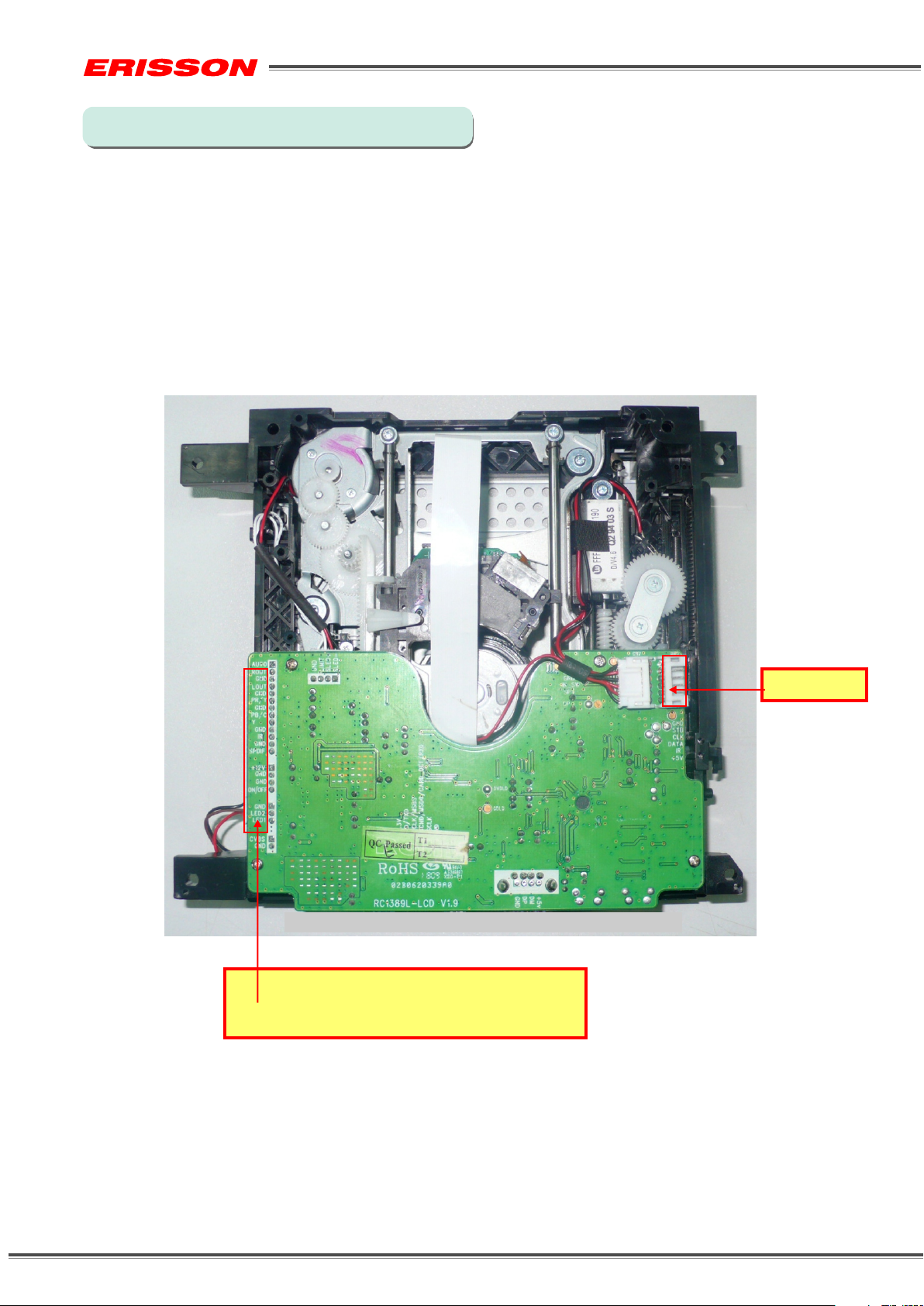
Illustration of actual object(5)
L22372E2801/22LDJ08
Name: DVD LOADER
Model No.:RC1389L-LCD V1.9
LC D-T V Ser vic e Man ual
CN3/CN8:
Motor Driver and Control Connector
KEY OUT
(25)
Page 26

Driver PCB Principle Diagram
LC D-T V Ser vic e Man ual
o
(26)
Page 27

2.AV-IN
LC D-T V Ser vic e Man ual
(27)
Page 28
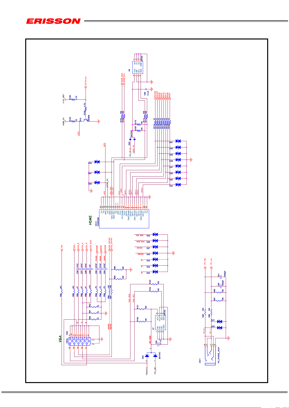
3.VGA&HDMI
LC D-T V Ser vic e Man ual
(28)
Page 29

4.TUNER
LC D-T V Ser vic e Man ual
(29)
Page 30
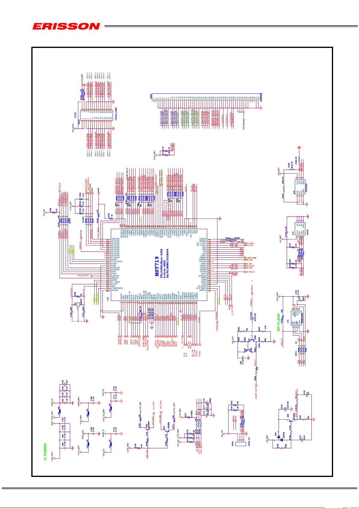
5.MST 719
LC D-T V Ser vic e Man ual
(30)
Page 31

6.SC7314
LC D-T V Ser vic e Man ual
(31)
Page 32

7.AUDIO AMP
LC D-T V Ser vic e Man ual
(32)
Page 33

8.KEY & IR
LC D-T V Ser vic e Man ual
(33)
Page 34

DVD PCB Principle Diagram
L22372E2801/22LDJ08
4
123
LIMIT_SW
SLED+
SLED-
220U/10V
EC1
104
C8
104
C4
+5V
NC/4.7K
R21
NC/4.7K
NC/2N3904
Q2
NC/2N3904
Q5
䝨
NC/10UF/10V
EC13
RESET
1 2
TS-6032ZJH
TS-6032ZJH
4P/P=2.0MM 90D
CN2
NC/15K
R33
132
_ꪘ
던
132
_ƈ
NC/22K
NC/4148
SW1
12
SW2
R20
NC/4.7K
R60
D3
H20
H21
H22
11223344556
IN_SW
SP+
SP-
R32
10K
R98
6P/P=2.0MM 90D
CN10
H19
47U/10V
104
10K
dെa
H18
LOAD+
EC11
C17
oa_fò
12345
H17
6P/P=2.0MM 90D
CN7
6
SPINDLE
FOCUS
LOAD-
R28
10K
VREF2
1
FOCUS_IN2TRB_13FB24SLED_IN5FB16CLOSE7OPEN8VCC9LOAD-10LOAD+11SLED+12SLED-13FOCUS-14FOCUS+
MUTE/STBY
TRACK_IN
TRB_325TRB_2
BIAS
24
26
27
28
100K
R36
TRACK
R37
10K
STANDBY
809S
_᎑
믘
1
+3.3V
2
RESET
RESET
R30
1K
C51
224
KEY1
KEY2
R97
+3.3V
paহa
pa됭ih
HPKPs
paM
6
CARD+3.3V
OPEN
CLOSE/DVD/CD
SPINDLE_IN
GND
22
23
SLED
U12
3
29
GND1
GND2
30
+3.3V
VFD_CLK
VFD_DATA
IR
M_D0
M_D1
M_D2
M_D3
M_D4
M_D5
M_D6
M_D7
M_DQM0
M_D15
M_D14
M_D13
M_D12
M_D11
M_D10
M_D9
M_D8
SP-
SP+
LOAD-
LOAD+
1R/0603
R2
10K
10K
FOCUS+
FOCUS-
R1
104C2104
C5
CD5888
U2
OP+
OP-
SPINDLE+18SPINDLE-
TRACK+16TRACK-
VCC1
VCTL
FB3
20
21
+5V+5V
1 1 TRAY BRAKE MODE
1 0 TRAY CLOSE MODE
0 1 TRAY OPEN MODE
PIN6(CLOSE) PIN7(OPEN) MODE
OPEN
LIMIT_SW
+3.3V
0 0 NO CONNECT MODE
+3.3V
IO_MUTE
R29
10K
33
GPIO3_/_INT#
34
GPIO4
35
GPIO6
36
SF_CS_
37
SF_DO
38
SF_DI
39
SF_CK
40
UP1_6_/_SCL
41
UP1_7_/_SDA
42
ICE
43
PRST#
44
IR
45
RD0
46
RD1
47
RD2
48
RD3
49
RD4
50
DVDD33
51
RD5
52
RD6
53
RD7
54
DVDD18
55
DQM0
56
RD15
57
RD14
58
RD13
59
RD12
60
DVSS33
61
RD11
62
RD10
63
RD9
64
RD8
+1.8V
15
17
19
TRACK-
TRACK+
SLED-
SLED+
SPI_CS
SPI_D0
SPI_D1
SPI_CLK
104
C22
100P
C16
100P
C13
100P
C11
R3
100P
C50
PIN6=PIN7=0 OR 1 when swap DVD/CD for OPU.
PIN6=PIN7=1 when reading CD DISC.
PIN6=PIN7=0 when reading DVD DISC.
+1.8V
5.1K
32
USB_V18
DQM166RCLK67RA11
65
TRACK
FOCUS
R38
R40
27K
27K
+3.3V
LED1_IN
CLOSE/DVD/CD
STANDBY
USB_DP
USB_DM
R52
23
24
GPIO_B/CLOSE/DVD/CD
TRO25FOO26FG_/_GPIO227GPIOK0/USB_DP28GPIOK1/USB_DM29USB_V3330USB_GND31GPIOK2/PAD_VRT
DVDD33
RA970RA8
RA4
RA572RA671RA7
69
74
68
73
H16
6
SLED
SPINDLE
153
C26
104
C24
330P
C23
330P
C25
R41
R39
10K
15K
+3.3V
DVDLDO
CDLDO
MT1389L
DVSS18
RA10
RAS#76CAS#75RWE#
BA178BA0
79
80
77
H13
H14
H15
VFD_STB
VFD_CLK
VREF2
MD
R48
15K
U6
81
H12
100R
R64
VFD_DATA
VREF2
13
V14
DVDD33
84
H11
12345
IR_IN
IR
VREF1
RA3
RA283RA182RA0
85
6P/P=2.0MM 90D
R25
R19
R14
R27
R43
R34
75R
75R
GPIO7_/_CKE
86
87
R95 33R
R94 33R
CN8
0R/0603
R15
10K
10K
10K
10K
C18
33P
27MHz
Y1
R35
1M
C28
33P
CBADFE+1.8V
+3.3V
5
4
1
RFE6RFF7AVDD188AVDD339XTALI10XTALO11AGND12V2014REXT15MDI116MDI217LDO118LDO219AVDD3320DMO21FMO22GPIO_A/STANDBY
RFD3RFC2RFB
RFA
RFH__/__OPINN
RFG_/__OPINP
RFIN_/_OPOUT
ADACVDD2
ADACVDD1
ALF_/_GPIO
ALS_/_GPIO
AL_/_GPIO1
AR_/_GPIO0
ARS_/_GPIO
ARF_/_GPIO
ADACVSS1
ADACVSS2
APLLCAP
APLLVDD
AKIN1_/_GPIO21_/_AUDIO_MUTE
ADVCM_/_GPIO20
AKIN2_/_GPIO19_/_AUDIO_MUTE
DACVDDA
DACVDDB
SPDIF_/_GPIO12
DACVSSC
DACVDDC
GPIO1390DVDD18
GPIO1191GPIO10
GPIO988GPIO8
VREF
94
93
92
89
96
95
C65
102
NC/0R/0603
RFIP
AGND18
AVDD18
AVCM
AADVDD
AADVSS
CVBS
R71
+3.3V
+5V
128
127
126
125
124
123
122
121
120
119
118
117
116
115
114
113
112
111
110
109
108
107
106
105
104
R
103
B
102
G
101
100
99
98
97
FS
DVDLD
Vdvd_ld:2.35V
10UH
L6
8550
Q9
베
_೬
132
Vr65:0.2V
5.1R/0603
47U/10V
R65
EC19
2.4V
DVDLDO
C37
104
RFO
OP+
OP-
C44
C47
105
220P
EC20
10U/25V
152
C57
A+3.3V
A+3.3V
560R
R90
1389L:VIDEO DAC
H-Impedance Mode:Rfs=2.2K Rload=150R
L-Impedance Mode:Rfs=560R Rload=37.5R
1389R:VIDEO DAC
L-Impedance Mode:Rfs=140R Rload=37.5R
V+3.3V
LC D-T V Ser vic e Man ual
104
CN4
OPU+5V
3P/P=2.0MM 90D
LED2_IN
U5 SPI FLASH-SOP8
C93
+5V
47U/10V
10UH
L3
EC12
OPU+5V
C27
104
C92
104
47U/10V
EC5
VREF1
104
C33
CN5
3.3V/0.5W
D5
104
C87
R82
10K
R87
10K
1K/0603
R9
P+12V
SPI_D0
SPI_CS
R61
1
10K
CE_B2DQ03WP#4GND
HOLD#
DQ16SCK
VDD
5
7
8
SPI_CLK
SPI_D1
+3.3V
FPC-24PIN(FOR HD65)
14F15B16A17RF18
F
GS
132
箸
1234567891011121314151617181920212223
CD/DVD
F-
19D20C21T-22T+23F+24
FOCUS-
FOCUS+
TRACK-
TRACK+
RFO
CDA
B
2SK3018
Q8
100K
R63
10K
R49
123
104
C89
104
C88
R76
1K
104
C7
LED1_IN
DVD_DET
+3.3V
SPI_CS
SPI_D0
1
CE_B2DQ03WP#4GND
U4
SPI FLASH-DIP8
HOLD#
DQ16SCK
VDD
5
7
8
SPI_CLK
SPI_D1
24
GND-LD2DVD-LD
VR-DVD
GND-PD
(N.C)
CD-LD
VR-CD
HFM
N.C
VCC
1
3
4
5MD6
7
8
9
10E11
12VC13
OPU+5V
Vmd:0.18V
CDLD
VREF1
0R
R62
MD
10UH
L7
_
132
47U/10V
EC21
CDLDO
+1.8V
+3.3V
FL
FR
KEY2
PR/R
PB/B
Y/G
CVBS
E
R58
0R
2SK3018
8550
Q11
Q7
R75
(RF+3.3V)
D
+3.3V
LED2_IN
IN_SW
D
GS
132
100K
R54
2N3904
Q6
_
132
R55
10K
CLOSE/DVD/CD:CD=1,DVD=0.
CLOSE/DVD/CD
R11
10K
壈
5.1R/0603
C72
104
SDCMD/MSD0/CARD_DET
SDCLK/MSBS
MSCLK
SD0
SD0
SDCLK/MSBS
SDCMD/MSD0/CARD_DET
MSCLK
CARD_DET=1,SD CARD
CARD_DET=0,MS CARD
+5V
USB_DM
USB_DP
0R/(FB 100M/100R)
1
2
D8
1
2
USB-A-06
1N4148
JK1
0R
R930RR92
L10
NC/BAV99
NC/10P
D7
C79
3
NC/10P
104
0R/1M
R96
NC/10P
C83
RQp
C80
3
RQp
C78
NC/BAV99
47U/10V
EC27
1
4
VBUS2DM3DP
GND
5
6
4P/P=2.0MM 90D
123
4
CN9
1
CD_SD
2
WP_SD
5
WP_GND_SD
4
DAT0_SD
3
DAT1_SD
22
DAT2_SD
20
CD/DAT3_SD
9
CLK_SD
17
CMD_SD
12
VDD_SD
14
VSS_SD
6
VSS_SD
23
CD_GND_SD
24
CD_GND_SD
25
CD_GND_SD
26
CD_GND_SD
7
VSS_MS
8
D9
10K
R78
10K
R77
47U/10V
104
104
BS_MS
10
MS_D1
11
SDIO_MS/MS_D0
13
MS_D2
15
INS_MS
16
MS_D3
18
SCLK_MS
19
VCC_MS
21
VSS_MS
27
28
EC24
C58
CARD+3.3V +3.3V
C59
10R/0603
R81
M_DQM1
NC/10P
C71
RAM_CLK
MSD-019-20-1090(PROCONN 3 IN 1)
JK2
ƈpN
ƈpO
ƈpP
ƈpQ
솈pR
ƈpS
쉈pU
枸pV
蜠pNM
M_A11
M_CAS
M_RAS
M_BA0
M_BA1
M_A9
M_A8
R89
33R
M_A10
M_A7
M_A6
M_A5
M_A4
M_WE
M_A0
M_A1
SDRAM 1Mx16x4
U7
10P
10P
M_A2
M_A3
C76
C77
SDCMD/MSD0/CARD_DET
SDCLK/MSBS
MSCLK
6
VSSQ12VSSQ46VSSQ52VSSQ
VDDQ9VDDQ43VDDQ49VDDQ
3
SD0
M_BA1
21
BA1
VDD27VDD28VSS41VSS
1
VFD_STB
SPDIF
KEY1
+3.3V
M_A11
RAM_CLK
M_RAS
M_WE
M_BA0
M_CAS
20
CAS18RAS15LDQM16WE19CS37CKE38CLK39UDQM
BA0
NC/RFU
VSS14VDD
NC
36
40
54
+3.3V
M_D14
M_D15
M_A2
M_A9
M_A8
M_A5
M_DQM1
M_DQM0
M_A10
M_A6
M_A4
M_A3
M_A0
M_A7
23A024A125A226A329A430A531A632A733A834A917
22
35
A10/AP
A11
D1047D1148D1250D1351D1453D15
2D04D15D27D38D410D511D613D742D844D945
M_D12
M_D13
M_D11
M_D10
M_D7
M_D1M_A1
M_D8
M_D3
M_D2
M_D0
M_D5
M_D4
M_D9
M_D6
26
50
SDRAM 16M-6(512Kx16x2)
VSS
VSS
U9
VSSQ
VSSQ
VSSQ
41
47
M_DQM1
M_DQM0
33
36
14
NC
DQMH37NC
DQML15WE
VCCQ
VCCQ
VSSQ
VCCQ
VCCQ
38
44
4
7
10
13
M_RAS
M_WE
M_CAS
16
34
CAS17RAS18CS19BA/A1120A10
CKE35CLK
DQ1449DQ15
VCC
VCC
25
48
1
M_D14
M_D15
+3.3V
RAM_CLK
M_D13
+3.3V
M_BA0
M_A2
M_A7
M_A9
M_A8
M_A5
M_A10
M_A6
M_A4
M_A3
M_A0
21A022A123A224
27A428A529A630A731A832
A3
A9
DQ1043DQ11
DQ1246DQ13
DQ840DQ9
DQ03DQ1
DQ26DQ3
DQ49DQ5
DQ612DQ7
39
42
45
M_D12
M_D11
2
5
8
11
M_D10
M_D7
M_D3
M_D2
M_D4
M_D9
M_D6
M_D1M_A1
M_D8
M_D0
M_D5
(34)
Page 35

LC D-T V Ser vic e Man ual
12V:500mA ,700mA MAX.
104
100K
NC/10K
NC/223
C6
R7
NC/100P
C9
910R
R6
SS14
D1
R60:51R
R59:3K
TD1410:VFB=1.22V
104
C86
104
C81
104
C82
220U/10V
EC4
C62
R8
51R
R5
4P/P=2.0MM 90D
CN1
4
R101
10K
7
EN
6
COMP
4
GND
FB
5
3K
R4
VIN
NC/TD1410
U1
SW
3
123
2
NC
47uH/CD75
NC/100K
104
104
100U/16V
EC2
104
BS
1
NC/103
L1
R100
C91
C55
104
100U/16V
EC29
C3
C90
8
C1
4.7uH/CD43 1A
L11
NC/0R/0805
P+12V
NC/FB 120R/0805
L9
R16
+5V
730MV
FR
10U/25V
EC15
8.2K
R50
C39
102
2.2K
R44
AVREF
150P
C29
2
3
U3-A
4558
R45
22K
1
10U/25V
EC8
AMUTE
R12
R101KR17
1K
2N3904
Q1
1
3
ƈ
2
ꇨ_
C10
102
1.85V
R13
47K
ROUT
75R
R74
100P
C45
1uH
100P
C41
75R
R72
100P
C15
PB/B_OUT
PR/R_OUT
10P
C19
1uH
L2
100P
C21
PR/R_OUTPR/R
ROUT
LOUT
DVD_DET
10P
C43
L5
Y/G_OUTY/G
Y/G_OUT
IR_IN
COAX
P+12V
104
100R/0603
100K
R23
C42
R59
47U/16V
EC9
100K
R57
104
C14
A+12V
AVREF
+5V
100K
R26
1N4148D41N4148
47U/10V
EC6
D2
220U/10V
EC14
132
10K
R31
2N3906
Q4
뾠_
꜠
10K
R22
SPDIF COAX
100R
R70
100R
R68
330P
C53
C49
0R
CVBS
75R
R91
100P
C74
10P
C67
1uH
L8
100P
C68
CVBS_OUT
2P/2.0MM
N
O
CN6
47U/10V
2N3906
FL
10U/25V
EC17
EC16
8.2K
R51
C40
102
2.2K
R46
AVREF
150P
C30
6
5
U3-B
4558
R47
22K
7
10U/25V
EC10
IO_MUTE
R24
1K
1K
+3.3V
2N3904
R69
1K
Q3
1
ƈ
3
軨_
132
2
Q10
C12
102
ᘀ_
ƈ
AMUTE
R18
47K
LOUT
75R
R73
100P
C34
10P
C31
1uH
L4
100P
C20
PB/B_OUTPB/B
13P/P=2.0MM 90D
1
DVD_DET2RO3GND4LO5GND6R/PR7GND8B9G/Y/SY10GND11IR12GND13COAX
CN3
RES0805:1/10W
RES0603:1/16W
RES0402:1/32W
RES1206:1/8W
C52
104
C54
104
C48
C63
104
C70
104
C60
104
C73
104
C75
104
104
104
104
47U/10V
EC22
C85
C84
C61
104
C64
104
C66
104
FB1
2R/0603
V+3.3V
47U/10V
104
104
EC18
C36
C69
47U/10V
(RF+3.3V)
+3.3V
+1.8V+1.8V +1.8V
C46
104
RF+1.8V
C38
104
+3.3V
15R/0603
R88
EC23
H6
22mA
A+3.3V
C56
104
FOR 12CM DISC FOR 8CM DISC
1.3V 1.3V50MA 50MA
H7
P+12V
1 2
LED1
470R/0603
R67
470R/0603
R66
1 2
LED2
H5
H4
H9
H8
4001
D11
4001
D10
P
sf䔐
1117-1.8V
ꁘag
U10
N
slrŎ
slr
220U/10V
EC26
O
Q
+1.8V
104
C35
47UF/10V
EC3
H1
H10
H3
H2
220U/10V
EC25
104
C32
47UF/10V
P
sf璘
1117-3.3V
饘ag
U8
N
slrŎ
slrŎ
O
Q
+3.3V
EC28
M1M2M3M4
(35)
Page 36
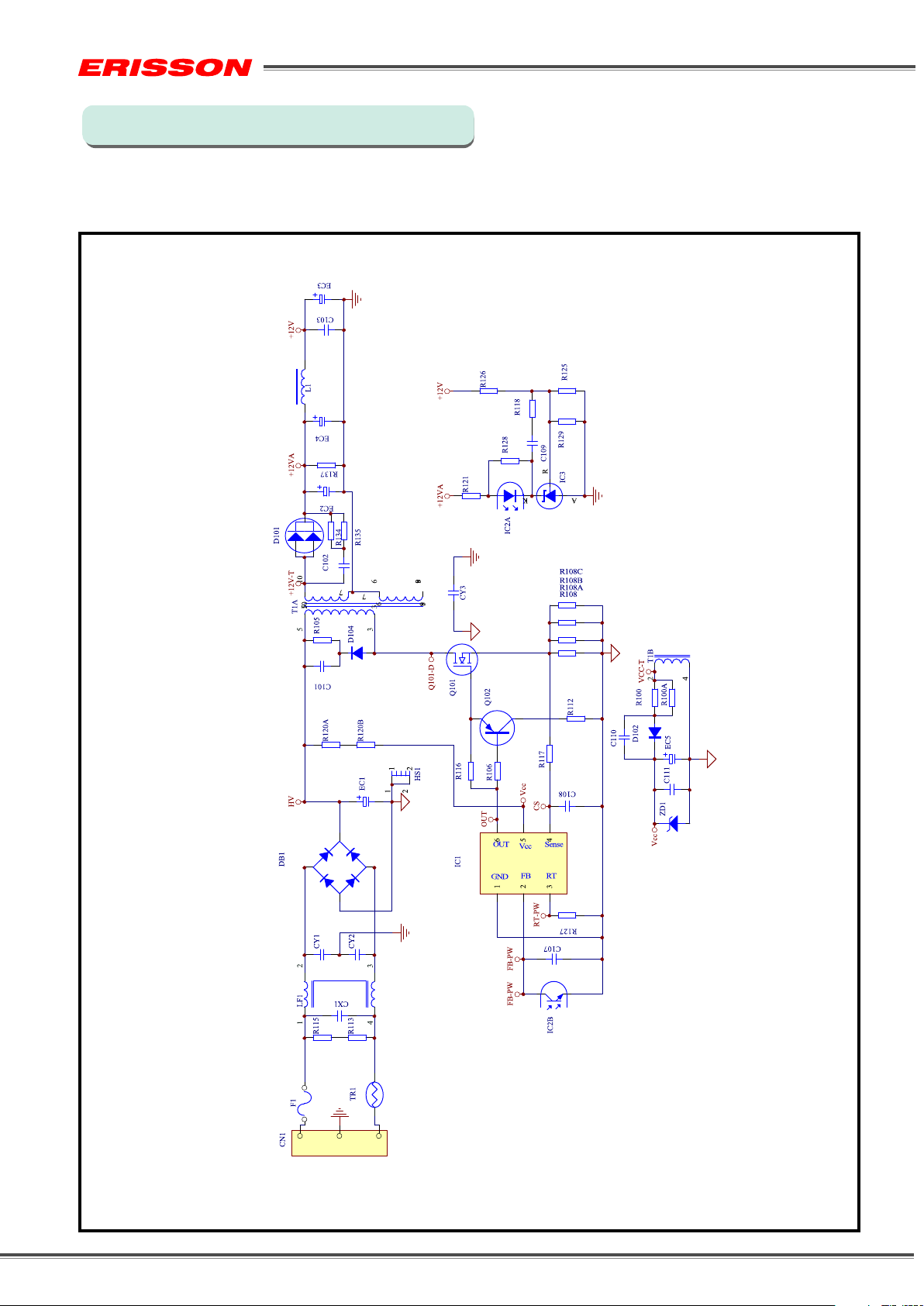
Power PCB Circuit Diagram(1)
L15372E2800/15LJ18
PCB Name: Power PCB
Power PCB Model No.:AYL150205X
Schematic(1)
LC D-T V Ser vic e Man ual
(36)
Page 37
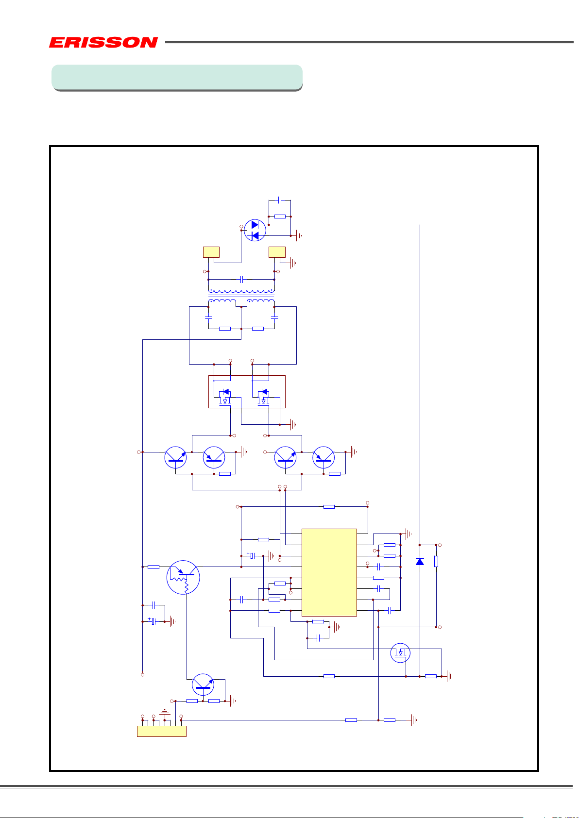
Power PCB Circuit Diagram(1-1)
L15372E2800/15LJ18
PCB Name: Power PCB
Power PCB Model No.:AYL150205X
Schematic(2)
D3
L1
3
1
2
CON2
H1
H
8 1
C19
C16
6
5
R25R24
LC D-T V Ser vic e Man ual
C6
R14
2
1
1
2
CON3
H2
2
L
T2
4
C18
5
D2
G2
4 6
Q6
+12VB
R15
C17C2
Q8
R5
VCC-INV
Q2
C3
S2
3
G1
7
D1D2D1
C4
8
U3
S1
G1
1
2
G2
Q5
CCE
+12VB
B
B
E2
E1
R16
C2
R18
Q7
E
R4
R26
E1
9
E2
10
C2
11
12
13
14
15
R10
Vref
16
U1
VCC
OUTPUTC
R6
VREF
A2-
A2+
R7
C13
C1
C1
8
GND
RT
CT
DTC
COMP
A1-
A1+
R12
7
Rt
6
Ct
R8
5
4
3
2
1
D1
C10
R9
C9
C20
Q4
CS-INV
R19
FB-INV
D1
D2
+12V
+12V1
+5V
2345678
Q1
R2
On/Off
R22
Adj
R23
R1
R13
R17
(37)
Page 38

Power PCB Circuit Diagram(2)
L19372E2800/19LJ08
PCB Name: Power PCB
Power PCB Model No.:LP220401
Schematic
LC D-T V Ser vic e Man ual
(38)
Page 39

Power PCB Circuit Diagram(3)
L22372E2801/22LDJ08
PCB Name: Power PCB
Power PCB Model No.:LK1060
LC D-T V Ser vic e Man ual
(39)
Page 40

Block Diagram(1)
L15372E2800/15LJ18
LC D-T V Ser vic e Man ual
REM OTE KEY B OAR D
DC
CON 2
CN1
AC IN
CON 2
(40)
Page 41
Block Diagram(2)
L19372E2800/19LJ08
LC D-T V Ser vic e Man ual
REMOTE K EY BO ARD
DC
CON 1
CN2
CN3
CON 2
AC IN
CON 4
CON 5
(41)
Page 42

Block Diagram(3)
L22372E2801/22LDJ08
LC D-T V Ser vic e Man ual
(42)
Page 43

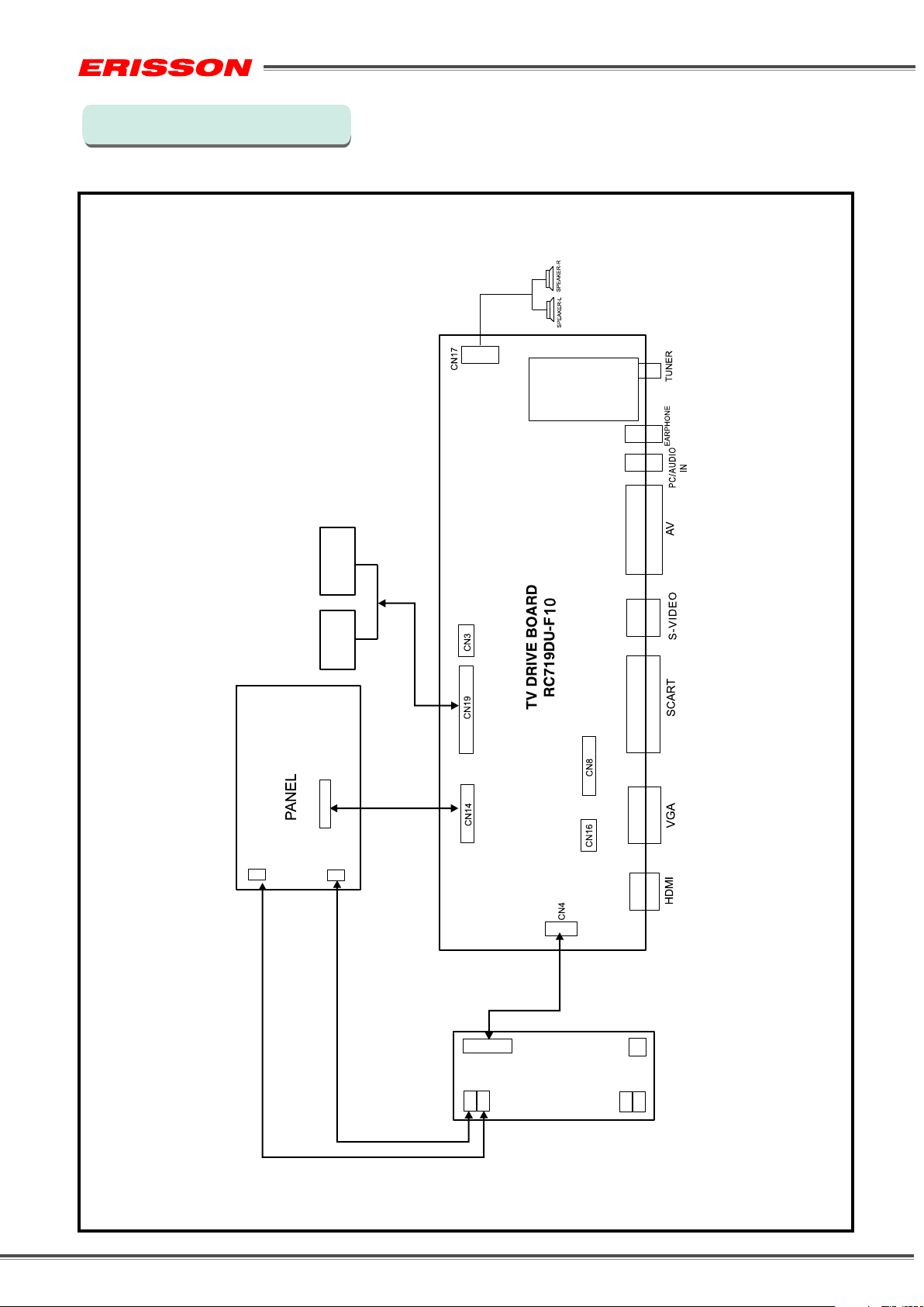
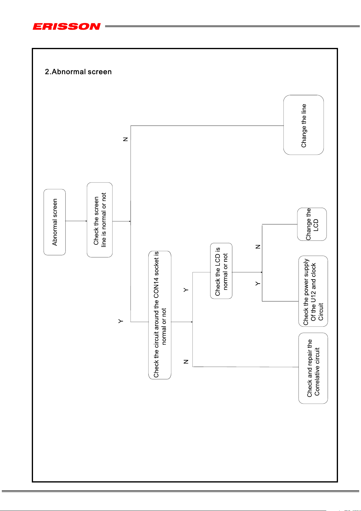
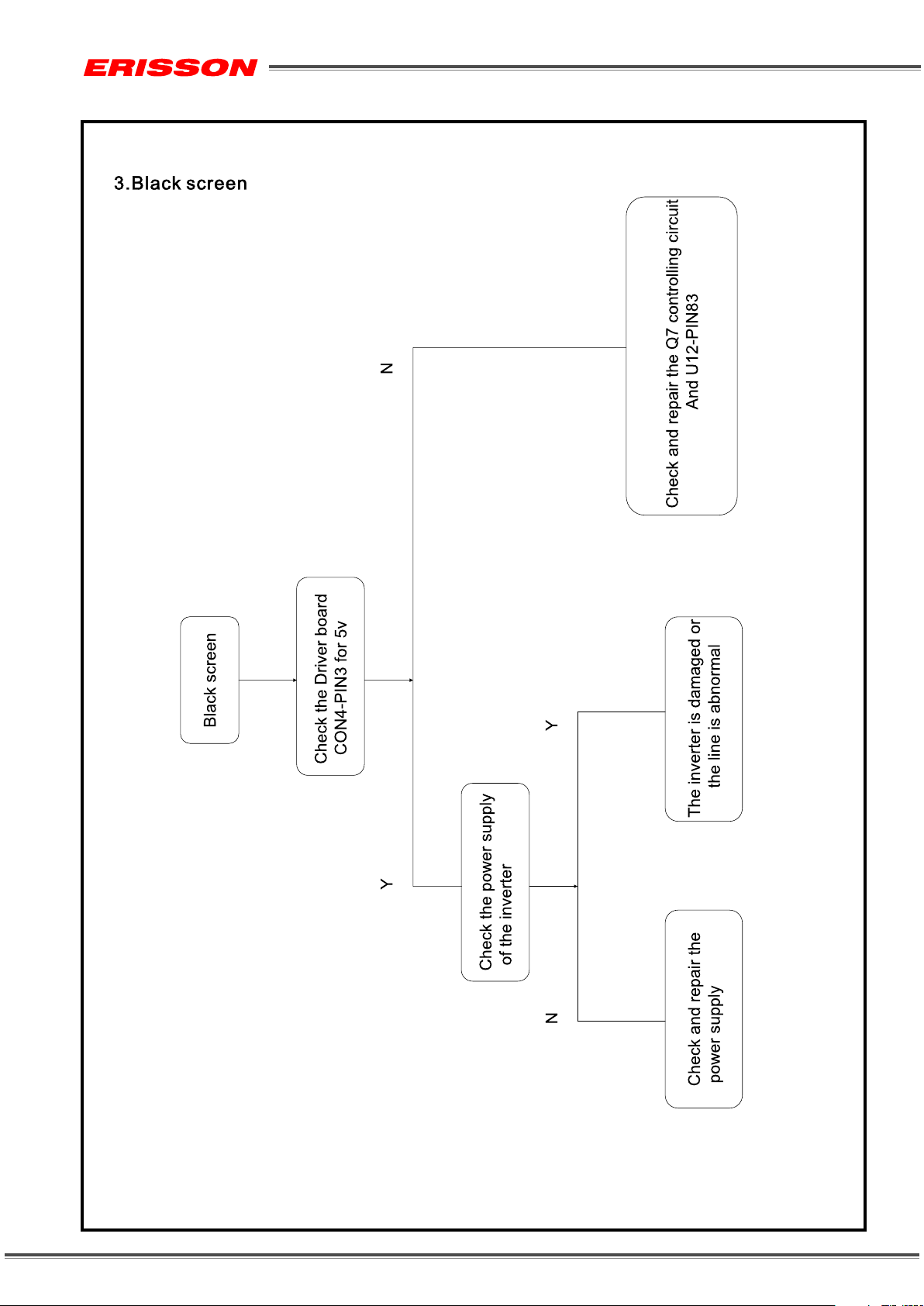
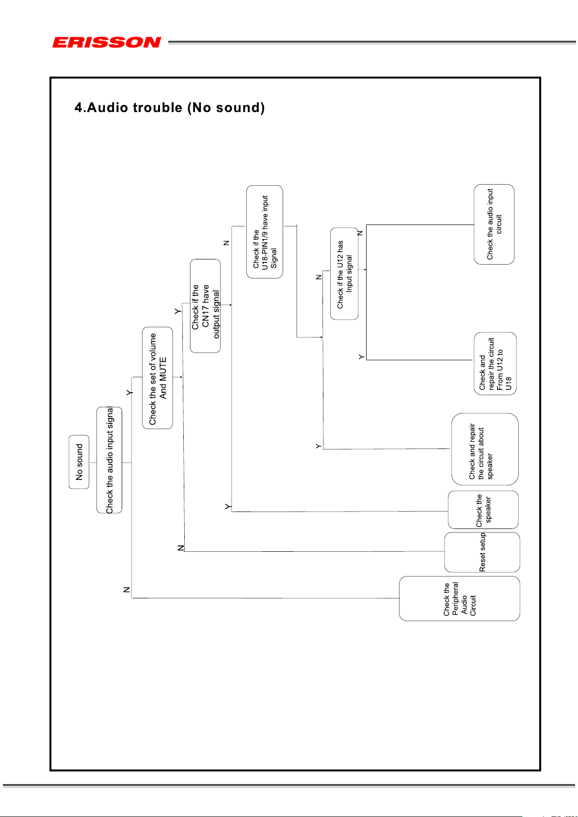
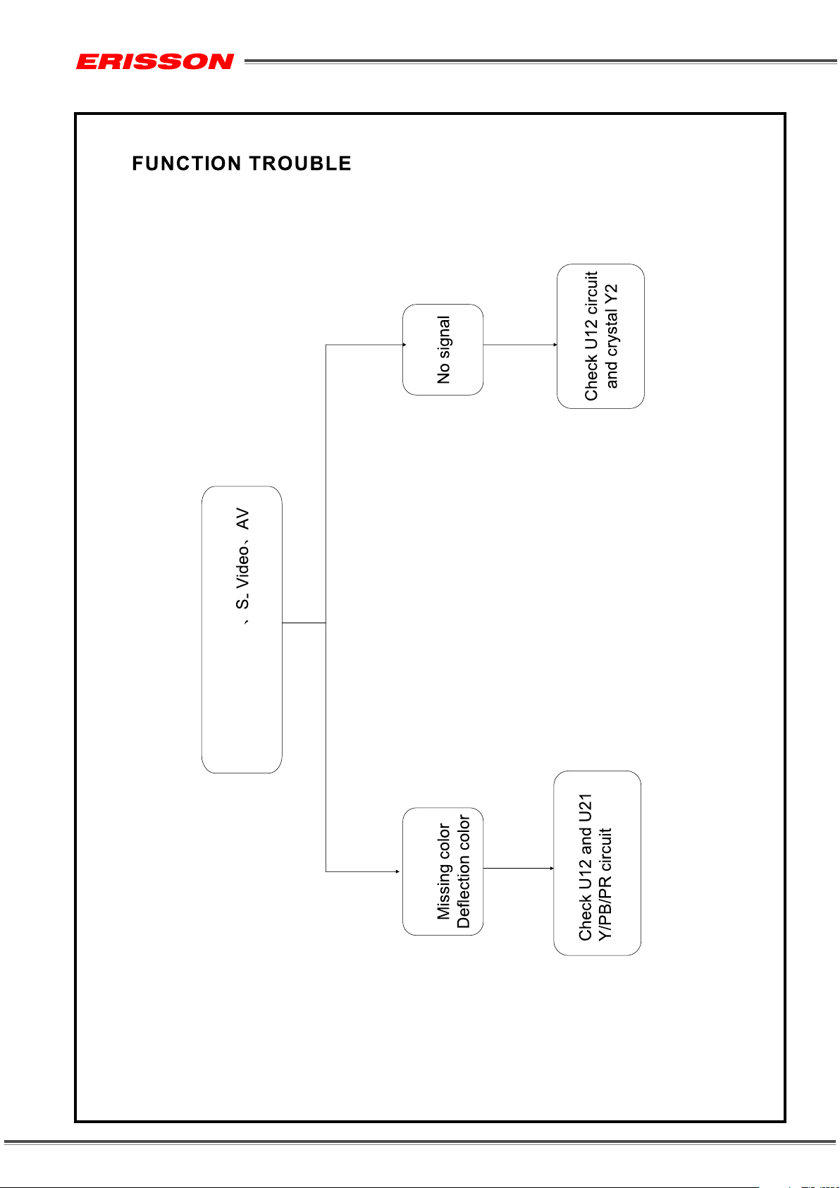
Trouble Shooting Charts
LC D-T V Ser vic e Man ual
(43)
Page 44
LC D-T V Ser vic e Man ual
(44)
Page 45
LC D-T V Ser vic e Man ual
(45)
Page 46
LC D-T V Ser vic e Man ual
(46)
Page 47

LC D-T V Ser vic e Man ual
(47)
Page 48

LC D-T V Ser vic e Man ual
(48)
Page 49

7.
LC D-T V Ser vic e Man ual
(49)
Page 50
LC D-T V Ser vic e Man ual
8.
(SCART/ YPbPr 、AV 、S-VIDEO)
SCART/YPbPr
SCART/YPbPr
(50)
Page 51

9.
LC D-T V Ser vic e Man ual
(51)
 Loading...