

Page 1

COLOR TELEVISION
SERVICE MANUAL
CHASSIS NO. ETA-1/ETA-1R
Please read this manual carefully before service.
Page 2

TABLE OF CONTENTS
SAFETY INSTRUCTIONS AND MAINTENANCE .......................................1
X-RAY RADIATION PRECAUTION.............................................................................…..........1
SAFETY PRECAUTION ...............................................................................................….........1
PRODUCT SAFETY NOTICE......................................................................................…..........2
SAFETY SYMBOL DESCRIPTION .............................................................................…..........3
MAINTENANCE............................................................................................................….........3
ADJUSTMENTS .......................................................................................................….......4
SET-UP ADJUSTMENTS .............................................................................................….........4
CIRCUIT ADJUSTMENTS............................................................................................….........7
STRUCTURE AND CHASSIS FUNCTION DESCRIPTION.............…..13
STRUCTURE BLOCK DIAGRAM ..................................................................................…......13
CHASSIS DESCRIPTION..........................................................................................……......14
SERVICE DATA.................................................................................................….....…....15
TECHNICAL DATA OF KEY ICS ............................................................................…....….....15
SERVICE DATA OF KEY ICS.................................................................................…....….....38
APPENDIX
CIRCUIT DIAGRAM
Page 3

SERVICE MANUAL
SAFETY INSTRUCTIONS AND MAINTENANCE
WARNING: BEFORE SERVICING THIS CHASSIS, READ THE “X-RAY RADIATION
PRECAUTION”, “SAFETY PRECAUTION”AND “PRODUCT SAFETY NOTICE”INSTRUCTION
BELOW.
X-RAY RADIATION PRECAUTION
1. The EHT must be checked every time the TV is serviced to ensure that the CRT does not emit
X-ray radiation as result of excessive EHT voltage. The maximum EHT voltage permissible in any
operating circumstances must not exceed the rated value. When checking the EHT, use the High
Voltage Check procedure in this manual using an accurate EHT voltmeter.
2. The only source of X-RAY radiation in this TV is the CRT. The TV minimizes X-RAY radiation,
which ensures safety during normal operation. To prevent X-ray radiation, the replacement CRT
must be
3. Some components used in this TV have safety related characteristics preventing the CRT from
emitting X-ray radiation. For continued safety, replacement component should be made after
referring the PRODUCT SAFETY NOTICE below.
4. Service and adjustment of the TV may result in changes in the nominal EHT voltage of the CRT
anode. So ensure that the maximum EHT voltage does not exceed the rated value after service
and adjustment.
identical to the original fitted as specified in the parts list.
SAFETY PRECAUTION
WARNING: REFER SERVICING TO QUALIFIED SERVICE PERSONNEL ONLY.
1. The TV has a nominal working EHT voltage. Extreme caution should be exercised when working
on the TV with the back removed.
1.1 Do not attempt to service this TV if you are not conversant with the precautions and procedures for
working on high voltage equipment.
1.2 When handling or working on the CRT, always discharge the anode to the TV chassis before
removing the anode cap in case of electric shock.
1.3 The CRT, if broken, will violently expel glass fragments. Use shatterproof goggles and take
extreme care while handling.
1.4 Do not hold the CRT by the neck as this is a very dangerous practice.
2. It is essential that to maintain the safety of the customer all power cord forms be replaced exactly
as supplied from factory.
3. Voltage exists between the hot and cold ground when the TV is in operation. Install a suitable
isolating transformer of beyond rated overall power when servicing or connecting any test
equipment for the sake of safety.
1
Page 4

SERVICE MANUAL
4. When replacing ICs, use specific tools or a static-proof electric iron with small power (below 35W).
5. Do not use a magnetized screwdriver when tightening or loosing the deflection yoke assembly to
avoid electronic gun magnetized and decrement in convergence of the CRT.
6. When remounting the TV chassis, ensure that all guard devices, such as nonmetal control buttons,
switch, insulating sleeve, shielding cover, isolating resistors and capacitors, are installed on the
original place.
7. Replace blown fuses within the TV with the fuse specified in the parts list.
8. When replacing wires or components to terminals or tags, wind the leads around the terminal
before soldering. When replacing safety components identified by the international hazard symbols
on the circuit diagram and parts list, it must be the company-approved type and must be mounted
as the original.
9. Keep wires away from high temperature components.
PRODUCT SAFETY NOTICE
CAUTION: FOR YOUR PROTECTION, THE FOLLOWING PRODUCT SAFETY NOTICE
SHOULD BE READ CAREFULLY BEFORE OPERATING AND SERVICING THIS TV SET.
1. Many electrical and mechanical components in this chassis have special safety-related
characteristics. These characteristics are often passed unnoticed by a visual inspection and the
X-ray radiation protection afforded by them cannot necessarily be obtained by using replacements
rated at higher voltages or wattage, etc. Components which have these special safety
characteristics in this manual and its supplements are identified by the international hazard
symbols on the circuit diagram and parts list. Before replacing any of these components read the
parts list in this manual carefully. Substitute replacement components which do not have the same
safety characteristics as specified in the parts list may create X-ray radiation.
2. Do not slap or beat the cabinet or CRT, since this may result in fire or explosion.
3. Never allow the TV sharing a plug or socket with other large-power equipment. Doing so may result
in too large load, causing fire.
4. Do not allow anything to rest on or roll over the power cord. Protect the power cord from being
walked on, modified, cut or pinched, particularly at plugs.
5. Do not place any objects, especially heavy objects and lightings, on top of the TV set. Do not install
the TV near any heat sources such as radiators, heat registers, stove, or other apparatus that
produce heat.
6. Service personnel should observe the SAFETY INSTRUCTIONS in this manual during use and
servicing of this TV set. Otherwise, the resulted damage is not protected by the manufacturer.
2
Page 5

SERVICE MANUAL
SAFETY SYMBOL DESCRIPTION
The lightning symbol in the triangle tells you that the voltage inside this product may
be strong enough to cause an electric shock. Extreme caution should be exercised
when working on the TV with the back removed.
This is an international hazard symbol, telling you that the components identified by
the symbol have special safety-related characteristics.
FDA This symbol tells you that the critical components identified by the FDA marking have
special safety-related characteristics.
UL This symbol tells you that the critical components identified by the UL marking have
special safety-related characteristics.
C UL This symbol tells you that the critical components identified by the C-UL marking
have been evaluated to the UL and C-UL standards and have special safety-related
VDE
characteristics.
This symbol tells you that the critical components identified by the VDE marking have
special safety-related characteristics.
MAINTENANCE
1. Place the TV set on a stable stand or base that is of adequate size and strength to prevent it from
being accidentally tipped over, pushed off, or pulled off. Do not place the set near or over a
radiator or heat register, or where it is exposed to direct sunlight.
2. Do not install the TV set in a place exposed to rain, water, excessive dust, mechanical vibrations or
impacts.
3. Allow enough space (at least 10cm) between the TV and wall or enclosures for proper ventilation.
4. Slots and openings in the cabinet should never be blocked by clothes or other objects.
5. Please power off the TV set and disconnect it from the wall immediately if any abnormal condition
are met, such as bad smell, belching smoke, sparkling, abnormal sound, no picture/sound/raster.
Hold the plug firmly when disconnecting the power cord.
6. Unplug the TV set from the wall outlet before cleaning or polishing it. Use a dry soft cloth for
cleaning the exterior of the TV set or CRT screen. Do not use liquid cleaners or aerosol cleaners.
3
Page 6

SERVICE MANUAL
ADJUSTMENTS
SET-UP ADJUSTMENTS
The following adjustments should be made when a complete realignment is required or a new picture
tube is installed.
Perform the adjustments in the following order:
1. Color purity
2. Convergence
3. White balance
Notes:
① The purity/convergence magnet assembly and rubber wedges need mechanical positioning.
② For some picture tubes, purity/ convergence adjustments are not required.
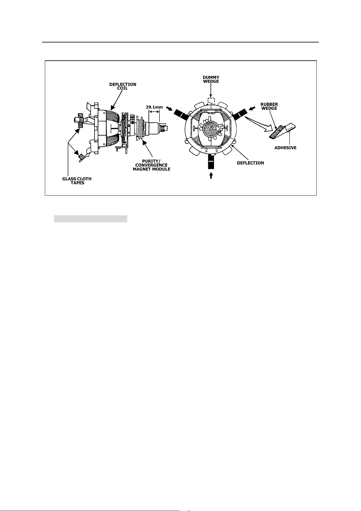
1. Color Purity Adjustment
Preparation:
Before starting this adjustment, adjust the vertical sync, horizontal sync, vertical amplitude and
focus.
1.1 Face the TV set north or south.
1.2 Connect the power plug into the wall outlet and turn on the main power switch of the TV set.
1.3 Operate the TV for at least 15 minutes.
1.4 Degauss the TV set using a specific degaussing coil.
1.5 Set the brightness and contrast to maximum.
1.6 Counter clockwise rotate the R /B low brightness potentiometers to the end and rotate the green
low brightness potentiometer to center.
1.7 Receive green raster pattern signals.
1.8 Loosen the clamp screw holding the deflection yoke assembly and slide it forward or backward to
display a vertical green zone on the screen. Rotate and spread the tabs of the purity magnet
around the neck of the CRT until the green zone is located vertically at the center of the screen.
1.9 Slowly move the deflection yoke assembly forward or backward until a uniform green screen is
obtained.
1.10 Tighten the clamp screw of the assembly temporarily. Check purity of the red raster and blue
raster until purities of the three rasters meet the requirement.
4
Page 7
SERVICE MANUAL
Yok
Fig. 1
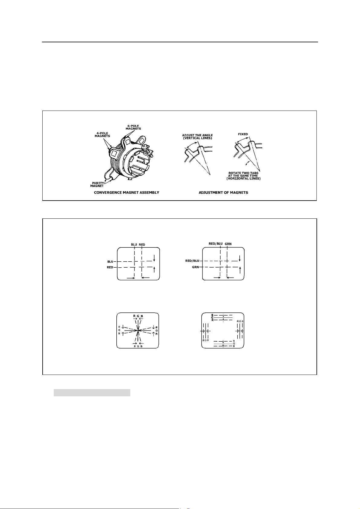
2. Convergence Adjustment
Preparation:
Before attempting any convergence adjustment, the TV should be operated for at least 15 minutes.
2.1 Center convergence adjustment
2.1.1 Receive dot pattern.
2.1.2 Adjust the brightness/contrast controls to obtain a sharp picture.
2.1.3 Adjust two tabs of the 4-pole magnet to change the angle between them and red and blue
vertical lines are superimposed each other on the center of the screen.
2.1.4 Turn both tabs at the same time keeping the angle constant to superimpose red and blue
horizontal on the center of the screen.
2.1.5 Adjust two tabs of the 6-pole magnet to superimpose red/blue line and green line.
2.1.6 Remember red and blue movement. Repeat steps 2.1.3~2.1.5 until optimal convergence is
obtained.
2.2 Circumference convergence adjustment
2.2.1 Loosen the clamp screw holding the deflection yoke assembly and allow it tilting.
2.2.2 Temporarily put the first wedge between the picture tube and deflection yoke assembly. Move
front of the deflection yoke up or down to obtain better convergence in circumference. Push the
mounted wedge in to fix the yoke temporarily.
2.2.3 Put the second wedge into bottom.
2.2.4 Move front of the deflection yoke to the left or right to obtain better convergence in
circumference.
2.2.5 Fix the deflection yoke position and put the third wedge in either upper space. Fasten the
5
Page 8
SERVICE MANUAL
deflection yoke assembly on the picture tube.
2.2.6 Detach the temporarily mounted wedge and put it in either upper space. Fasten the deflection
yoke assembly on the picture tube.
2.2.7 After fastening the three wedges, recheck overall convergence and ensure to get optimal
convergence. Tighten the lamp screw holding the deflection yoke assembly.
Fig. 2
4-pole Magnet Movement 6-pole Magnet Movement
Center Convergence by Convergence Magnets
Incline the Yoke Up (or Down) Incline the Yoke Right (or Left)
Circumference Convergence by DEF Yoke
3. White Balance Adjustment
Fig.3
Generally, white balance adjustment is made with professional equipment. It’s not practical to get
good white balance only through manual adjustment. For TVs with I
data to adjust white balance.
2
C bus control, change the bus
6
Page 9
SERVICE MANUAL
CIRCUIT ADJUSTMENTS
Preparation:
Circuit adjustments should be made only after completion of set-up adjustments.
Circuit adjustments can be performed using the adjustable components inside the TV set. For TVs with
2
C bus control, first change the bus data.
I
1. Degaussing
A degaussing coil is built inside the TV set. Each time the TV is powered on, the degaussing coil
will automatically degauss the TV. If the TV is magnetized by external strong magnetic field,
causing color spot on the screen, use a specific degausser to demagnetize the TV in the following
ways. Otherwise, color distortion will be shown on the screen.
1.1 Power on the TV set and operate it for at least 15 minutes.
1.2 Receive red full-field pattern.
1.3 Power on the specific degausser and face it to the TV screen.
1.4 Turn on the degausser. Slowly move it around the screen and slowly take it away from the TV.
1.5 Repeat the above steps until the TV is degaussed completely.
2. Confirmation and Adjustment for Voltage
Caution: +B voltage has close relation to high voltage. To prevent X-ray radiation, set +B voltage to
the rated value.
2.1 Make sure that the supply voltage is within the range of the rated value.
2.2 Connect a digital voltmeter to the voltage output terminal of the main PCB. Power on the TV and set
the brightness and sub-brightness to minimum. Ensure that the voltage from the main PCB reads as
follows.
2.3 Regulate voltage adjustment components on the power section until the +B the voltage reaches the
rated value.
Table 1
Test Point Voltage (V) Test Point Voltage (V)
TP-130V
TP-17V
TP-5V-1
TP-11V
TP-200V
130V±1.5V
17V±1V
5V±0.3V
11V±1V
190V±5V
TP-18V
TP-5V-2
TP-8V
TP-26V
20V±1V
5V±0.3V
8V±0.5V
26V±1V
Note:
It’s impossible to check the power part separately from the main chassis board as the part is
mounted on the main chassis board. The power components, etc. should be checked for
burnout when power-on. If burned out, do not power on the TV again until the cause is found
out.
7
Page 10
3. High Voltage Inspection
Measure voltages of test points on the main PCB with the digital voltmeter. Measure the CRT
high voltage with the high-voltage testing equipment and heater voltage with the high-frequency
effective voltmeter. The rated values are shown as below.
Table 2
Test Point Voltage (V)
Negative of VD461 26±1V
Negative of VD485 190±5V
CRT anode 27±1.5KV
Heater 6.3±0.3Vrms
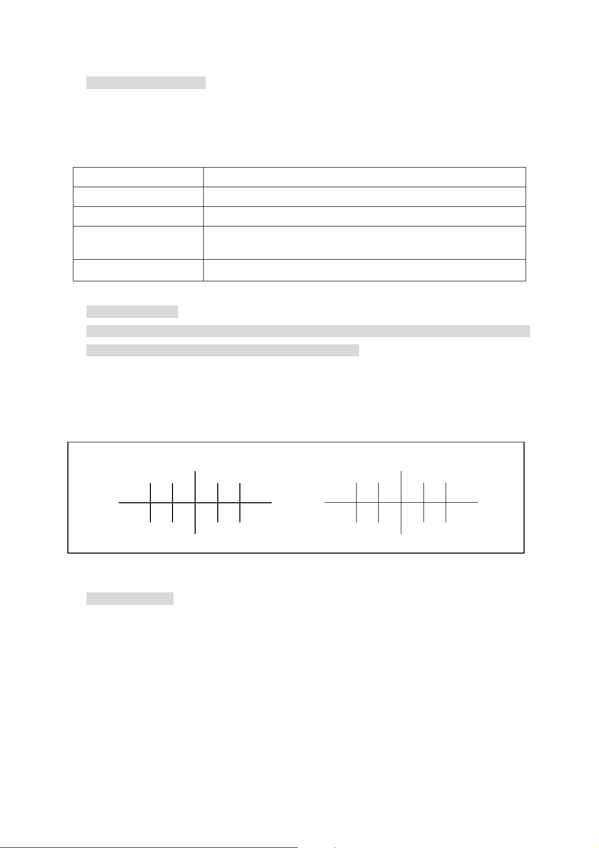
4. Focus Adjustment
Caution: Dangerously high voltages are present inside the TV. Extreme caution should be
exercised when working on the TV with the back removed.
4.1 After removing the back cover, look for the FBT on the main PCB. There should be a FCB on
the FBT.
4.2 Power on the TV and preheat it for 15 min.
4.3 Receive a normal TV signal. Rotate knob of the FCB until you get a sharp picture.
Before Adjusting After Adjusting
Fig. 4
5. Safety Inspection
5.1 Inspection for insulation and voltage-resistant
Perform safety test for all naked metal of the TV. Supply high voltage of 3000V AC, 50Hz (limit
current of 10mA) between all naked metal and cold ground. Test every point for 3 sec. and
ensure no arcing and sparking.
5.2 Requirements for insulation resistance
Measure resistance between naked metal of the TV and feed end of the power cord to be
infinity with a DC-500 high resistance meter and insulation resistance between the naked metal and
8
Page 11
SERVICE MANUAL
degaussing coil to be over 20MΩ.
6. SERVICE mode
6.1 To enter the DESIGN/SERVICE mode
Set the volume to 0. Then press and hold the MUTE button on the remote control, and press the
MENU button on the TV to enter the SERVICE mode. In this case, red “s” is displayed on the
upper center of the screen. To exit from the S mode, turn off the TV set by the POWER button
on the remote control.
Caution: The user service mode adjustment can be changed only when service personnel adjust
the whole set data during servicing. As the control data have dramatic effects on functions and
performance of the TV, service personnel should not tell user how to enter the SERVICE mode
to avoid improper data settings.
6.2 Adjustments and bus data (GDET0101-07 for ETA-1/GDET0102-02 for ETA-1R)
Table 3 Function Description for Bus Data
Symbol Description Data
OSD OSD Horizontal Position 29
OPT Optional Setting B3
RCUT R CUT OFF OPT
PAGE1
PAGE2
PAGE3
PAGE4
GCUT G CUT OFF OPT
BCUT B CUT OFF OPT
GDRV G DRIVE OPT
BDRV B DRIVE OPT
SCNT SUB CONTRAST 05
CNTN CONTRAST MIN 0A
CNTC CONTRAST CENTER 3B
CNTX CONTRAST MAX 7A
CNTD CONTRAST MAX IN DVD F7
BRTN BRIGHT MIN.(difference from center) 20
BRTC BRIGHT CENTER 40
BRTX BRIGHT MAX.(difference from center) 20
BRTS SUB BRIGHT FB
COLC COLOR CENTER NTSC 33
COLP
COLD COLOR CENTER DVD 05
COLN COLOR MIN. 0D
COLX COLOR MAX.(difference from center) 45
TNTN TINT MIN.(difference from center) 28
TNTC TINT CENTER 40
TNTX TINT MAX.(difference from center) 28
ST3 SHARP CENTER 3.58NTSC TV 19
ST4 SHARP CENTER OTHER TV 19
SV3 SHARP CENTER 3.58NTSC VIDEO 1D
SV4 SHARP CENTER OTHER VIDEO 1D
SVD SHARP CENTER DVD 1B
ASSH ASYMMETRY-SHARPNESS 05
COLOR CENTER PAL(difference from
COLC)
02
(continued)
9
Page 12
PAGE5
PAGE6
PAGE7
PAGE8
PAGE9
PAGE10
SERVICE MANUAL
SHPN SHARP MIN(difference from center) 10
SHPX SHARP MAX(difference from center) 16
ABCL ABL date in detail 0C
DCBS A part of Video date in detail 15
CLTB
CLTD
CLTM
CLVO
CLVD
OSDA OSD ABL and OSD CONTRAST 01
HPOS Horizontal Position OPT
HPS
VP50 Vertical Position 50Hz OPT
VP60 Vertical Position 60Hz OPT
HIT Hight 50Hz OPT
HITS Hight 60Hz(difference from HIT) OPT
VLIN V Linearity 50Hz OPT
VLIS V Linearity 60Hz(difference from VLIN) OPT
VSC VS Correction 50Hz OPT
VSS VS Correction 60Hz OPT
HBOW OPT
HPARA OPT
UBLACK 0B
VBLACK 0B
AGC RF AGC 30
HAFC AFC GAIN 86
NOIS 0F
NDTC Noise detection count test 1F
MUTT Y-MUTE FOR SOFT START 00
STAT CONTRAST UP FOR SOFT START 00
VL1 ALC off volume control level 09
VL25 No use 3D
VL50 No use 57
VLX No use 7F
VA1
VA12 No use 25
VA25 No use 3D
VA50 No use 57
VAX No use 7F
SVM MON/SVM CO MAX SVM DL SVM GAIN 10
VBLK V BLK start V BLK stop 00
VCEN V CENTERING 17
VB1
VB25 No use 3D
VB50 No use 57
VBX No use 7F
FLG0 FLAGS for IF 44
FLG1 FLAGS 00
UCOM Miciom control 00
The date when TV mode & SOUND SYS
= B/G
The date when TV mode & SOUND SYS
= D/K
The date when TV mode & SOUND SYS
= M
The date when YUV mode & SOUND
SYS != M
The date when YUV mode & SOUND
SYS = M
Horizontal Position 60Hz(difference from
HPOS)
volume level when ALC on(IC
VER1.2_old)
volume level when ALC on(IC
VER1.2_new)
8A
86
AC
AD
88
OPT
19
09
(continued)
10
Page 13
SERVICE MANUAL
OSDF OSD PLL DATE 6A
TB_COL Menu top OSD area plane color set 9B
BB_COL Menu itmes OSD area plane color set BD
CL_COL1 Calendar OSD color 02
PAGE11
PAGE12
PAGE13
PAGE14
PAGE15
PAGE16
PAGE17
CL_COL2 Calendar OSD color 02
PYNX Normal H.SYNC max 33
PYNN Normal H.SYNC min 11
PYXS Search H.SYNC max
PYNS Search H.SYNC min 1E
RCUTS R cut offset in DVD 00
GCUTS G cut offset in DVD 00
BCUTS B cut offset in DVD 00
GDRVS 00
BDRVS 00
AUSTP 04
BBCT 04
STBG S TRAP B/G 06
STI S TRAP I 08
STDK S TRAP D/K 08
STM S TRAP M 01
SSBG S TRAP HP/LP B/G 08
SSI S TRAP HP/LP I 08
SSDK S TRAP HP/LP D/K 08
SSM S TRAP HP/LP M 09
SYNC 04
SYBBN BB judgement 00
SYBBF BB judgement 00
SYSR Set WIN Pulse and HLOCK Pulse 20
VCD0 00
VCD1 00
BL25 Balance 25 1E
BL49 Balance 49 50
MODE0 29
MODE1 0F
OV50 00
OV60 00
HOTEL 00
FM RADIO 01
SOUND M 01
SCR SAV 01
ENGLISH 01
FRENCH 01
GERMAN 01
RUSSIAN 00
INDONESIAN 01
MALAY 01
KOREA 01
ARABIC 00
INITIAL 00
LOCK MENU 01
CALENDAR 01
INFOMENU 01
DEMOKEY 01
SVIDEO 01
DVDVIDEO 01
LOGO 00
22
(continued)
11
Page 14
SERVICE MANUAL
LOGO1COLOR OPT
LOGO2COLOR OPT
LOGO1LINE OPT
PAGE18
PAGE19
Notes:
LOGO2LINE OPT
LOGO1SIZE OPT
LOGO2SIZE OPT
LG1 OPT
LG2 OPT
SBY 08
SRY 08
SECD 10
SEC29 00
ZOOMOFFSET OPT
① The data sheet may differ dependent on different models.
② The data sheet may differ dependent on different CRTs for the same model.
③ PAGE19 for ETA-1R Chassis Series only.
12
Page 15

Page 16

SERVICE MANUAL
2. CHASSIS DESCRIPTION
General Description
ETA-1 chassis is applied in SF21GA63 series.
By use of Toshiba V/C/D-MCU 2IN1 IC for TV small signal processing and bus control,
the chassis enables TV tuning, adjustment, control and picture correction, featuring
high-integration, high-performance-to-price ratio and high-reliability and compact circuit
with fewer external components. The chassis, widely used in small and medium TVs,
provides much more convenience for manufacturing and technical service. It includes:
● 2IN1 IC TMPA88xxPSANG-4VB6 for PAL/NTSC small signal processing and bus control
● EEPROM AT24C16 for data memory
● LA78040 for vertical output power amplifying
● TFA9842AJ for audio power amplifying
● Thick-film IC STR-G5653 for power circuit adjustment and control
The following features are available in the chassis:
● Color systems: PAL, NTSC
● Sound systems: D/K B/G I M
● 236 programs preset
● AV stereo
● I2C bus control
● Electronic program table
● Intelligent lock
● Biorhythm
● Calendar inquiry
The chassis mainly uses the following ICs and assemblies.
Table 5 Key ICs and Assemblies
Serial
No.
Position Type Description
1 N201 AT24C16 EERPOM
2 N202
GDET0101-07/0102-02
(TMPA88xxPSANG)
2IN1 IC (Small signal processor +
micro control unit (MCU))
3 N603 TFA9842AJ Audio power amplifier
4 N301 LA78040 Vertical scan output stage circuit
5 N801 STR-G5653
Switch-mode power supply
control
6 A001 TAF5-C4I21 Tuner
14
Page 17

SERVICE MANUAL
SERVICE DATA
TECHNICAL DATA OF KEY ICS
1.MCU and Signal Processor for a PAL/NTSC TV
TMPA88xxCMANG /CPANG/CRANG /CSANG
1.General Description
The TMPA88xxCPANG is an integrated circuit for a PAL/NTSC TV. A MCU and a TV signal processor are
integrated in a 64-pin shrink DIP package. The MCU contains 8-bit CPU, ROM, RAM, I/O ports,
timer/counters, A/D converters, an on-screen display controller, remote control interfaces, IIC bus interfaces
and the Closed Caption decoder. The TV signal processor contains PIF, SIF, Video, multi-standard chroma,
Sync, RGB processors.
Mask ROM: TMPA88xxCMANG (ROM size: 32k)
Mask ROM: TMPA88
Mask ROM: TMPA88xxCRANG (ROM size: 56k)
Mask ROM: TMPA88xxCSANG (ROM size: 64k)
OTP ROM: TMPA88xxPSANG (ROM size: 64k)
Weight: 8.85 g (typ.)
xxCPANG (ROM size: 48k)
15
Page 18

SERVICE MANUAL
2.Features
MCU CCD Decoder
●High speed 8-bit CPU (TLCS-870/X series) ●Digital data slicer for NTSC
●Instruction execution time: 0.5 s (at 8 MHz)
●(TMPA88xxCPANG) ●Clock generation for OSD display
48-Kbytes ROM, 2-Kbytes RAM
●ROM correction ●Font ROM characters: 384 characters
●12 I/O ports ●Characters display: 32 columns ×12 lines
●14-bit PWM output 1 ch for a voltage synthesizer ●Composition: 16 ×18 dots
●7-bit PWM output 1 channel ●Size of character: 3 (line by line)
●8-bit A/D converter 3 ch for a touch-key input with ●Color of character: 8 (character by character)
key ON wake-up CIRCUIT
●Remote control signal preprocessor ●BOX function
●Two 16-bit internal timer/counter 2 ch ●Fringing, smoothing, Italic, underline function
●Two 8-bit internal timer/counter 2 ch ●Conform to CCD REGULATION
OSD
●Clock generation for OSD display
●Display position: H 256/V 512 steps
●Time base timer, watchdog timer ●Jitter elimination
●16 interrupt sources: external 5, internal 11
IIC bus interface (multi-master)
●STOP and IDLE power saving modes
TV Processor
IF RGB/Base-Band
●Integrated PIF VCO aligned automatically ●Integrated 1 H base-band delay line
●Negative demodulation PIF ●Base-band TINT control
●Multi-frequency SIF demodulator without external ●Internal OSD interface
Tank-coil
●SIF BPF built-in ●External YCbCr interface for DVD
●SIF Trap filter built in ●RGB cut-off/drive controls by bus
Video
●Integrated chroma traps
●Black stretch ●Integrated fH ×640 VCO
●Y-gamma ●DC coupled vertical ramp output (single)
●Half-tone and transparent for OSD
●ABCL (ABL and ACL combined)
Sync.
Chroma
●Integrated chroma BPFs
●PAL/NTSC demodulation ●2 for video
or 1 for audio (Stereo, 2ch ATT), controlled by IIC bus
●Sync output
AV Switch
●2 for audio(mono)
●ALC (Auto-Audio Level Control)
16
Page 19

3.Block Diagram
SERVICE MANUAL
17
Page 20

SERVICE MANUAL
4.Basic Structure
1. Internal Connections
TMPA88xx has two pieces of IC chip in one package, using Multi-Chip-Package (MCP) technology.
One is a micro controller (MCU) and the other one is a signal processor (SP) for a color TV. There
are some internal connections between these two ICs for handling below signals.
Signal Name Direction Description
1 SCL M to S Internal IIC bus SCL
2 SDA Bi-direction Internal IIC bus SDA
3 OSD R M to S OSD signal connection
4 OSD G M to S OSD signal connection
5 OSD B M to S OSD signal connection
6 OSD Y/BL M to S OSD display control
7 OSD I, CS OUT M to S OSD half-tone control/Test pattern signal
8 C-Video S to M Composite video signal from internal video switch, for CCD
9 C-Sync S to M Composite sync. signal from sync. Separator, for CCD
10 HD S to M Horizontal timing pulse regenerated from FBP, for OSD
11 VD S to M Vertical timing pulse from sync. Separator, for OSD
12 CLK M to S 8 MHz clock
13 AVDD M to S Reference voltage for C-Video interface
14 ADC S to M A/D converter monitoring RF-AGC, R-Y and B-Y
Functions of SP from MCU are controllable through the IIC bus of the internal connections.
2. Power Supply
TMPA88xx has some power supplies and GND pins. Power supplies related MCU must be applied at
the first. Power supplies for H.VCC and TV D.VCC are the second with at least 100 ms delay after
MCU power ON. The other power supplies are the last, which are recommended to be supplied from a
regulator circuit using FBP.
3. Crystal Resonator
TMPA88xx requires only one crystal resonator, in stead that a conventional two-chip solution
requires two resonators at least, one for MCU and the other one for SP. An oscillation clock with the
crystal resonator of TMPA88xx is supplied for MCU operation, PIF VCO automatic alignment,
alignment free AFT, chroma demodulation and horizontal oscillation. The oscillation frequency is
very important so that those of functions work properly, so that designing the oscillation frequency
accurately is required. The spec of crystal is recommended to be within
fosc: 8 MHz +/−20 ppm
ftemp: 8 MHz +/−40 ppm (−20°C to +65°C)
While RESET of MCU is active, the MCU function stops. Hardware and software initialization
sequence including power supplies control is required, because status of any hardware after the
RESET period is unknown especially horizontal oscillator which is a very basic timing generator of SP
operation.
18
Page 21

5.TERMINAL INTERFACE
SERVICE MANUAL
19
Page 22

SERVICE MANUAL
20
Page 23

SERVICE MANUAL
21
Page 24

SERVICE MANUAL
22
Page 25

SIGNAL PROCESSOR BLOCK
SERVICE MANUAL
23
Page 26

SERVICE MANUAL
24
Page 27

SERVICE MANUAL
25
Page 28

SERVICE MANUAL
26
Page 29

SERVICE MANUAL
27
Page 30

SERVICE MANUAL
Microcontrollers Descriptions (MROM version: TMPA88xxCMANG /CPANG /CRANG /CSANG)
28
Page 31

SERVICE MANUAL
2. TFA9842AJ
2-channel audio amplifier with volume control (SE: 1 W to 7.5 W)
1. General description
The TFA9842AJ contains two identical audio power amplifiers. The TFA9842AJ can be used as two
Single-Ended (SE) channels with a volume control. The maximum gain is 26 dB.
The TFA9842AJ comes in a 9-pin DIL-bent-SIL (DBS9P) power package. The TFA9842AJ is pin compatible
with the TFA9843AJ, TFA9843(B)J, TFA9842(B)J and TFA9841J. The difference between the TFA9843AJ
and the TFA9843(B)J,TFA9842(B)J, TFA9841J is the functionality of pin 7. The TFA9843AJ has a Volume
Control (VC) on pin 7. The TFA9843(B)J, TFA9842(B)J and TFA9841J have a mode select (Mode) on pin 7.
The TFA9842AJ contains a unique protection circuit that is solely based on multiple temperature
measurements inside the chip. This gives maximum output power for all supply voltages and load conditions
with no unnecessary audio holes. Almost any supply voltage and load impedance combination can be made
as long as thermal boundary conditions (number of channels used, external heatsink and ambient
temperature) allow it.
2. Features
■ 2 Channel SE: 1 W to 7.5 W operation possibility
■ Soft clipping
■ Input clamps
■ Volume control
■ Standby and mute mode
■ No on/off switching plops
■ Low standby current
■ High supply voltage ripple rejection
■ Outputs short-circuit protected to ground, supply and across the load
■ Thermally protected
■ Pin compatible with the TFA9843AJ, TFA9843(B)J, TFA9842(B)J, TFA9841J.
3. Applications
■ CRT TV, LCD TV
■ Monitors
■ PC speakers
■ Boom box
■ Mini and micro audio receivers.
29
Page 32

3. Block diagram
SERVICE MANUAL
4. Pinning information
4.1 Pinning
30
Page 33

4.2 Pin description
SERVICE MANUAL
31
Page 34

SERVICE MANUAL
4. VERTICAL SCAN OUTPUT STAGE CIRCUIT LA78040/LA78041
Both LA78040/LA78041 are vertical scan output stage power amplifiers. But there is a little
bit difference between the two amplifiers, that is, LA78040 has supply voltage of 24V and output
current of 1.8AP-P while LA78041 has supply voltage of 30V and output current of 2.2AP-P.
LA78040/LA78041 (N602)
Vertical Deflection Output Circuit
1) Features
Low power dissipation due to built-in pump-up circuit
Vertical output circuit
Thermal protection circuit built in
Excellent crossover characteristics
DC coupling possible
Package Type:TO-220-7H
Fig.12
2) Block Diagram
Fig.1 3 Block diagram
32
Page 35

SERVICE MANUAL
5. EEPROM AT24C04/08/16
1) Features
Low-voltage and Standard-voltage Operation
-2.7 (Vcc=2.7V to 5.5V)
-1.8 (Vcc=1.8V to 5.5V)
Internally Organized 128x8(1K), 256x8 (2K), 512x8 (4K),
1024x8 (8K) or 2048x8 (16K)
2-wire Serial Interface
Schmitt Trigger, Filtered Inputs for Noise Suppression
Bi-directional Data Transfer Protocol
100kHz (1.8V, 2.5V, 2.7V) and 400 kHz (5V) Compatibility
Write Protect Pin for Hardware Data Protection
8-byte Page (1K, 2K), 16-byte Page (4K, 8K, 16K) Write Modes
Partial Page Writes are Allowed
Self-timed Write Cycle (10 ms max)
High-reliability
-Endurance: 1 Million Write Cycles
- Data Retention: 100 Years
Automotive Grade and Extended Temperature Devices Available
8-lead PDIP, 8-lead JEDEC SOIC, 8-lead MAP and 8-lead TSSOP Package
2-wire
Serial EEPROM
AT24C01A 1K (128 x 8)
AT24C02 2K (256 x 8)
AT24C04 4K (512 x 8)
AT24C08 8K (1024 x 8)
AT24C16 6K (2048 x 8)
2) Description
The AT24C01A/02/04/08/16 provides 1024/2048/4096/8192/16384 bits of serial electrically erasable
and programmable read-only memory (EEPROM) organized as 128/256/512/1024/2048 words of 8 bits
each. The device is optimized for use in many industrial and commercial applications where low-power
and low-voltage operations are essential. The AT24C01A/02/04/08/16 is available in space-saving
8-pin PDIP, 8-lead JEDEC SOIC, 8-lead MAP and 8-lead TSSOP packages and is accessed via a
2-wire serial interface. In addition, the entire family is available in 2.7V (2.7V to 5.5V) and 1.8V (1.8V to
5.5V) versions.
33
Page 36

SERVICE MANUAL
A
A
A
A
A
A
A
A
A
A
A
A
3) Pin Configuration
Table 12
8-lead TSSOP
8-lead MAP
Pin Name Function
A0-A2 Address Inputs
SDA Serial Data
SCL Serial Clock Input
WP Write Protect
0
1
2
GND
VCC
WP
SCL
SDA
1
2
3
4
VCC
1
2
3
4
8
WP
7
SCL
6
SDA
5
0
8
1
7
2
6
GND
5
NC No Connect
Bottom View
Fig. 14
8-pin PDIP
8-lead SOIC
VCC
0
GND
1
1
2
2
3
4
8
WP
7
SCL
6
SDA
5
0
1
2
GND
1
2
3
4
VCC
8
WP
7
SCL
6
SDA
5
Fig. 15
4) Pin Description
SERIAL CLOCK (SCL): The SCL input is used to positive edge clock data into each EEPROM device
and negative edge clock data out of each device.
SERIAL DATA (SDA): The SDA pin is bi-directional for serial data transfer. This pin is open-drain
driven and may be wire-ORed with any number of other open-drain or open-collector devices.
DEVICE/PAGE ADDRESSES (A2, A1, A0): The A2, A1 and A0 pins are device address inputs that are
hard wired for the AT24C01A and the AT24C02. As many as eight 1K/2K devices may be addressed
on a single bus system (device addressing is discussed in detail under the Device Addressing section).
The AT24C04 uses the A2 and A1 inputs for hard wire addressing and a total of four 4K devices may
be addressed on a single bus system. The A0 pin is a no connect.
The AT24C08 only uses the A2 input for hardwire addressing and a total of two 8K devices may be
addressed on a single bus system. The A0 and A1 pins are no connects.
The AT24C16 does not use the device address pins, which limits the number of devices on a single bus
to one. The A0, A1 and A2 pins are no connects.
WRITE PROTECT (WP): The AT24C01A/02/04/16 has a Write Protect pin that provides hardware data
34
Page 37

SERVICE MANUAL
protection. The Write Protect pin allows normal read/write operations when connected to ground (GND).
When the Write Protect pin is connected to Vcc, the write protection feature is enabled and operates as
shown in table 14.
Table 13
WP Pin
Status
At Vcc Full (1K)
At GND Normal Read/Write Operations
5) Memory Organization
AT24C01A, 1K SERIAL EEPROM: Internally organized with 16 pages of 8 bytes each, the 1K requires
a 7-bit data word address for random word addressing.
AT24C02, 2K SERIAL EEPROM: Internally organized with 32 pages of 8 bytes each, the 2K requires
an 8-bit data word address for random word addressing.
AT24C04, 4K SERIAL EEPROM: Internally organized with 32 pages of 16 bytes each, the 4K requires
a 9-bit data word address for random word addressing.
AT24C08, 8K SERIAL EEPROM: Internally organized with 64 pages of 16 bytes each, the 8K requires
a 10-bit data word address for random word addressing.
AT24C16, 16K SERIAL EEPROM: Internally organized with 128 pages of 16 bytes each, the 16K
requires an 11-bit data word address for random word addressing.
6) Block Diagram
Part of the Array Protected
24C01A 24C02 24C04 24C08 24C16
Array
Full (2K)
Array
Full (4K)
Array
Normal
Read/
Write
Operation
Upper
Half
(8K)
Array
Fig.16
7) Refer to Table 21 about Functions and Data of the IC’s Pins.
35
Page 38

SERVICE MANUAL
7. SWITCH-MODE POWER SUPPLY IC STRG5653/G8656
1). General Description
The STRG5653/G8656 are part of the STRG5600/G8600 series thick-film ICs for switch-mode
power supply incorporating power MOSFET with a high-precise error amplifier. The ICs feature
fewer external components, small-size and standard power supply.
The series STR-G8600 use Chip on Chip technology with the same operation principle as
STR-G5600. Pin configuration, function and threshold of STR-G8600 are compatible with those of
STR-G5600.
2) Block Diagram
3) Function of Terminal
Terminal
No.
1 D Drain Terminal MOS FET drain
2 S Source Terminal MOS FET source
3 GND Ground Terminal Ground
4 VIN Power supply Terminal Input of power supply for control
5 O.C.P/F.B Overcurrent/Feedback
Symbols Description Functions
Fig.18
Table 15 Function of Terminal
Terminal
signals
Input of overcurrent detection signal
and constant voltage signals
4) Refer to Table 22 about Functions and Data of the IC’s Pins.
36
Page 39

SERVICE MANUAL
protection. The Write Protect pin allows normal read/write operations when connected to ground (GND).
When the Write Protect pin is connected to Vcc, the write protection feature is enabled and operates as
shown in table 14.
Table 13
WP Pin
Status
At Vcc Full (1K)
At GND Normal Read/Write Operations
5) Memory Organization
AT24C01A, 1K SERIAL EEPROM: Internally organized with 16 pages of 8 bytes each, the 1K requires
a 7-bit data word address for random word addressing.
AT24C02, 2K SERIAL EEPROM: Internally organized with 32 pages of 8 bytes each, the 2K requires
an 8-bit data word address for random word addressing.
AT24C04, 4K SERIAL EEPROM: Internally organized with 32 pages of 16 bytes each, the 4K requires
a 9-bit data word address for random word addressing.
AT24C08, 8K SERIAL EEPROM: Internally organized with 64 pages of 16 bytes each, the 8K requires
a 10-bit data word address for random word addressing.
AT24C16, 16K SERIAL EEPROM: Internally organized with 128 pages of 16 bytes each, the 16K
requires an 11-bit data word address for random word addressing.
6) Block Diagram
Part of the Array Protected
24C01A 24C02 24C04 24C08 24C16
Array
Full (2K)
Array
Full (4K)
Array
Normal
Read/
Write
Operation
Upper
Half
(8K)
Array
Fig.16
7) Refer to Table 21 about Functions and Data of the IC’s Pins.
37
Page 40

SERVICE DATA OF KEY ICS
Table 16 Ground Resistance of TMPA88xx Pins
SERVICE MANUAL
Pin No
Resistance
Pin No
Resistance
Pin No
Resistance
Pin No
Resistance
Pin No
Resistance
Pin No
Resistance
1 2 3 4 5 6
>2000 KΩ >2000 KΩ
7 8 9 10 11 12
>2000 KΩ
13 14 15 16 17 18
-
19 20 21 22 23 24
>2000 KΩ >2000 KΩ >2000 KΩ 107 KΩ 93.2 KΩ 3.2 KΩ
25 26 27 28 29 30
0.56 KΩ 24.70 KΩ 16.65 KΩ 22.04 KΩ 0.3 KΩ 3.27 KΩ
31 32 33 34 35 36
3.2 KΩ 107 KΩ >2000 KΩ >2000 KΩ 1500 KΩ 1.9 KΩ
0
>2000 KΩ >2000 KΩ 18.6 KΩ 10.6 KΩ
- 0
>2000 KΩ
5.6 KΩ >2000 KΩ
0 0
>2000 KΩ
0
Pin No
Resistance
Pin No
Resistance
Pin No
Resistance
Pin No
Resistance
Pin No
Resistance
Note: Measured when Power-off
37 38 39 40 41 42
>2000 KΩ 100 KΩ >2000 KΩ
43 44 45 46 47 48
14.5 KΩ 220 KΩ 3.2 KΩ >2000 KΩ 1.9 KΩ
49 50 51 52 53 54
0.7 KΩ 69 KΩ 120 KΩ 69 KΩ
55 56 57 58 59 60
- - - - -
61 62 63 64
>2000 KΩ
-
>2000 KΩ
0
-
56 KΩ 56 KΩ
0 -
>2000 KΩ
-
38
Page 41

SERVICE MANUAL
Table 17 Operating Voltage of TMPA88xx(N202)’s Pins
Pin No
Voltage (V)
Pin No
Voltage (V)
Pin No
Voltage (V)
Pin No
Voltage (V)
Pin No
Voltage (V)
Pin No
Voltage (V)
1 2 3 4 5 6
0V 0V 5V GND 5V 2.3V
7 8 9 10 11 12
2.1V GND 5V GND GND 1.1V
13 14 15 16 17 18
2.2V 5.9V 4.1V 4.7V 8.3V 0V
19 20 21 22 23 24
3.2V 2.4V 3.2V 3.8V 2.5V 2.5V
25 26 27 28 29 30
0V 2.7V 4.5V 3.2V 3.2V 3.0V
31 32 33 34 35 36
1.5V 3.9V 3.0V 3.1V 2.4V 5V
Pin No
Voltage (V)
Pin No
Voltage (V)
Pin No
Voltage (V)
Pin No
Voltage (V)
Pin No
Voltage (V)
37 38 39 40 41 42
2.0V 3.9V 3.0V GND 0V 2.0V
43 44 45 46 47 48
1.4V 2.6V 2.8V 2.3V 5.0V 4.5V
49 50 51 52 53 54
3.4V 2.5V 2.5V 2.5V GND GND
55 56 57 58 59 60
5V 0V 5V 5V 0V 5.0V
61 62 63 64
0V 4.5V 0.9V 0V
39
Page 42

Pin
No.
SERVICE MANUAL
Table 18 Functions and Service Data of TFA9842AJ’s Pins
Symbol Functions Description
Reference
Voltage(V)
Digital Multimeter
Positive Resistance(20K
Ω)
1 IN2 Input 2 4.7
2 OUT2 Loudspeaker terminal 2 9.0
Common input voltage
3 CIV
4.7
decoupling
4 IN1 Input 2 4.7
5 GND ground 0 0
Half supply voltage
6 SVR
10.4 -
decoupling(ripple rejection)
Volume control input(standby,
7 VC
20
mute and volume control)
8 OUT1 Loudspeaker terminal 1 9 -
9 VCC supply voltage 20
18.2MΩ
28KΩ
280KΩ
18.2MΩ
11KΩ
1KΩ
40
Page 43

SERVICE MANUAL
Table 21 Functions and Service Data of AT24C08/16 Pins
Pin No. Function Description
Reference Voltage
(V)
Digital Multimeter
Positive
Resistance
Negative Resistance
(20KΩ)
(20KΩ)
1 Address input 0 0 0
2 Address input 0 0 0
3 Address input 0 0 0
4 Common ground 0 0 0
5 Clock line 5 13.79 11.22
6 Data line 5 13.70 13.13
7 PW write protect 0 0 0
8 Supply voltage 5 3.79 3.78
Table 22 Functions and Service Data of STR-G5653’s Pins
Digital Multimeter
Pin
Functions Description
No.
Reference Voltage
(V)
Positive Resistance (20K
Ω)
Negative Resistance
(20KΩ)
1 Drain terminal 288
2 Source terminal 0.028 0 0
3 Ground terminal 0 0 0
4 Power supply terminal 32.24
Overcurrent/Freedback
5
terminal
1.85 0.68 0.68
∞ ∞
∞
1.838
41
Page 44

TMPA88xx N202
1. Any components identified by have special safety-related characteristics.
Use replacement Which have the same characteristics as original parts.
2. Cold ground Hot ground
This circuit diagram is only for reference, specifications are subject to change without reference.
Circuit Diagram FOR SF21GA63
TAF5-C4I23
BSC60 2
J
 Loading...