

Page 1

Mobile Communications
MASTR II
MAINTENANCE MANUAL
406-420 & 512 MHz,
40-WATT TRANSMITTER
Maintenance Manual
LBI-4622B
Printed in U.S.A.
Page 2
Copyright © 1974 General Electric Company
TABLE OF CONTENTS
Page
DESCRIPTION . . . . . . . . . . . . . . . . . . . . . . . . . . . . . . . . . . . . . . . . . . . . . . . . . . . . . 2
CIRCUIT ANALYSIS . . . . . . . . . . . . . . . . . . . . . . . . . . . . . . . . . . . . . . . . . . . . . . . . . . 2
Exciter . . . . . . . . . . . . . . . . . . . . . . . . . . . . . . . . . . . . . . . . . . . . . . . . . . . . . . . 2
ICOMS . . . . . . . . . . . . . . . . . . . . . . . . . . . . . . . . . . . . . . . . . . . . . . . . . . 2
Audio IC . . . . . . . . . . . . . . . . . . . . . . . . . . . . . . . . . . . . . . . . . . . . . . . . . 3
Buffer, Phas e Modulators & Amplifiers . . . . . . . . . . . . . . . . . . . . . . . . . . . . . . . . . 3
Buffer, Multi plie rs & Amplifier . . . . . . . . . . . . . . . . . . . . . . . . . . . . . . . . . . . . . 3
Power Amplifier . . . . . . . . . . . . . . . . . . . . . . . . . . . . . . . . . . . . . . . . . . . . . . . . . . 3
RF Amplifiers . . . . . . . . . . . . . . . . . . . . . . . . . . . . . . . . . . . . . . . . . . . . . . 4
Power Control Circuit . . . . . . . . . . . . . . . . . . . . . . . . . . . . . . . . . . . . . . . . . . 4
Carrier Control Timer . . . . . . . . . . . . . . . . . . . . . . . . . . . . . . . . . . . . . . . . . . . . . . . 4
MAINTENANCE . . . . . . . . . . . . . . . . . . . . . . . . . . . . . . . . . . . . . . . . . . . . . . . . . . . . 4
Disassembly . . . . . . . . . . . . . . . . . . . . . . . . . . . . . . . . . . . . . . . . . . . . . . . . . . . . 4
PA Transistor Replacement . . . . . . . . . . . . . . . . . . . . . . . . . . . . . . . . . . . . . . . . . . . . 5
Alignment Procedure . . . . . . . . . . . . . . . . . . . . . . . . . . . . . . . . . . . . . . . . . . . . . . . 7
Test Procedures . . . . . . . . . . . . . . . . . . . . . . . . . . . . . . . . . . . . . . . . . . . . . . . . . . 8
Power Output . . . . . . . . . . . . . . . . . . . . . . . . . . . . . . . . . . . . . . . . . . . . . . 8
Tone Deviation . . . . . . . . . . . . . . . . . . . . . . . . . . . . . . . . . . . . . . . . . . . . . . 8
V oice Deviation . . . . . . . . . . . . . . . . . . . . . . . . . . . . . . . . . . . . . . . . . . . . . 8
Troubleshooting . . . . . . . . . . . . . . . . . . . . . . . . . . . . . . . . . . . . . . . . . . . . . . . . . . 10
OUTLINE DIAGRAM . . . . . . . . . . . . . . . . . . . . . . . . . . . . . . . . . . . . . . . . . . . . . . . . . 12
SCHEMATIC DIAGRAMS
Exciter . . . . . . . . . . . . . . . . . . . . . . . . . . . . . . . . . . . . . . . . . . . . . . . . . . . . . . . 16
Power Amplifier . . . . . . . . . . . . . . . . . . . . . . . . . . . . . . . . . . . . . . . . . . . . . . . . . . 18
PARTS LIST AND PRODUCTION CHANGES
Exciter . . . . . . . . . . . . . . . . . . . . . . . . . . . . . . . . . . . . . . . . . . . . . . . . . . . . . . . 14
Power Amplifier . . . . . . . . . . . . . . . . . . . . . . . . . . . . . . . . . . . . . . . . . . . . . . . 20 thru 23
ILLUSTRATIONS
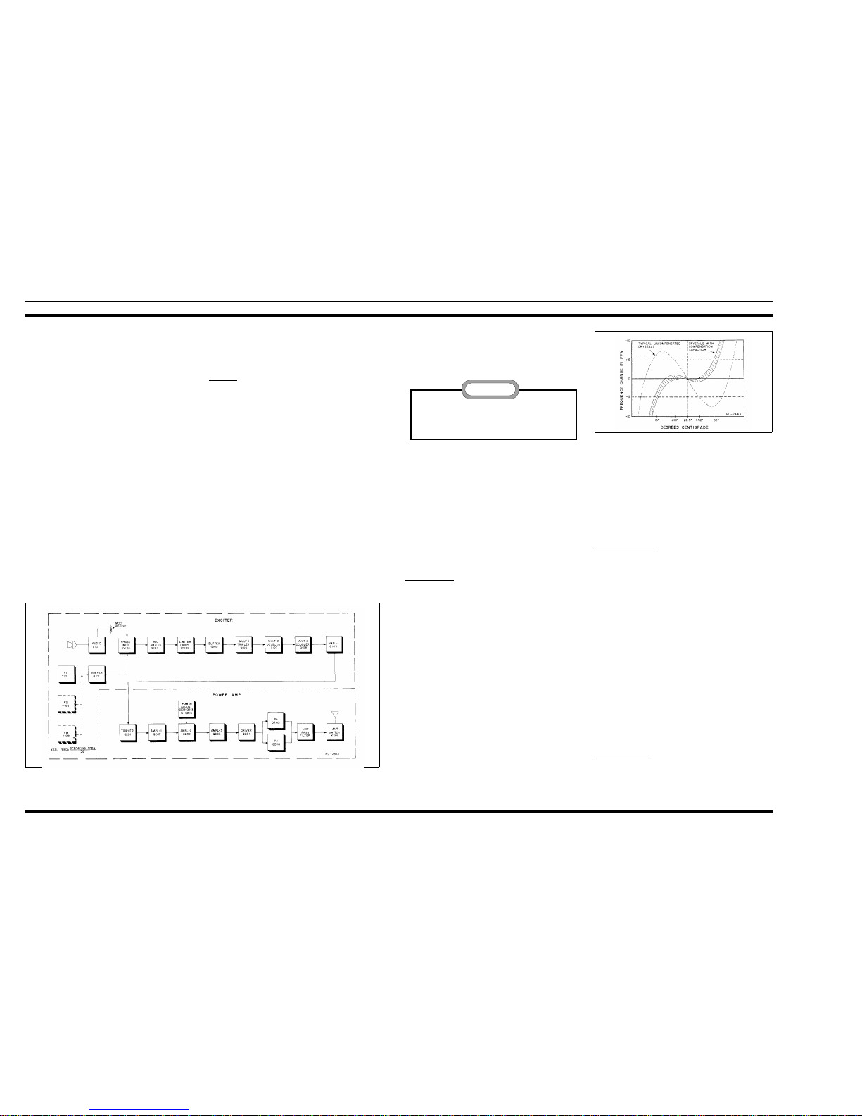
Figure 1 - Block Diagram . . . . . . . . . . . . . . . . . . . . . . . . . . . . . . . . . . . . . . . . . . . . . . . . 1
Figure 2 - Typical C rystal Characteristics . . . . . . . . . . . . . . . . . . . . . . . . . . . . . . . . . . . . . . . . 2
Figure 3 - Equivalent ICOM Circuit . . . . . . . . . . . . . . . . . . . . . . . . . . . . . . . . . . . . . . . . . . 3
Figure 4 - Simplified Audio IC . . . . . . . . . . . . . . . . . . . . . . . . . . . . . . . . . . . . . . . . . . . . . 3
Figure 5 - Disassembly Procedure ( Top View) . . . . . . . . . . . . . . . . . . . . . . . . . . . . . . . . . . . . . 4
Figure 6 - Disassembly Procedure (Bottom View) . . . . . . . . . . . . . . . . . . . . . . . . . . . . . . . . . . . 4
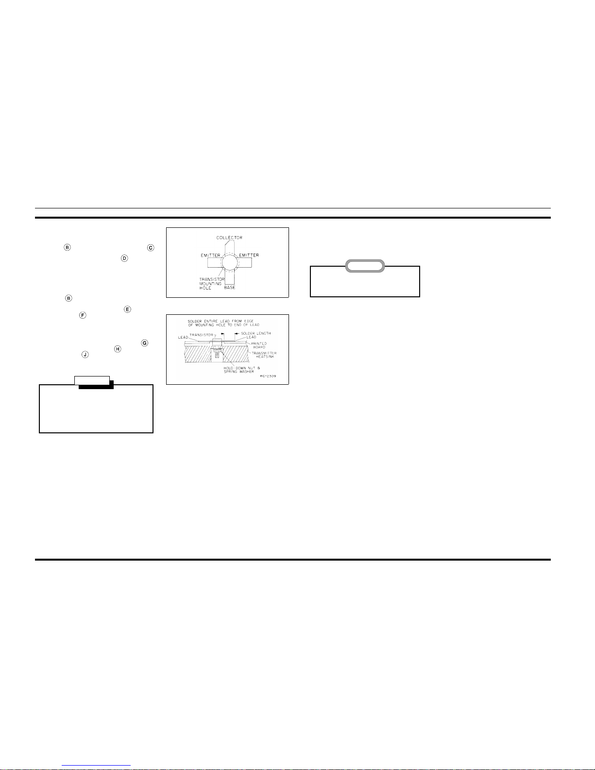
Figure 7 - PA Transistor Lead Identification . . . . . . . . . . . . . . . . . . . . . . . . . . . . . . . . . . . . . . 5
Figure 8 - PA Transistor Lead Forming . . . . . . . . . . . . . . . . . . . . . . . . . . . . . . . . . . . . . . . . . 5
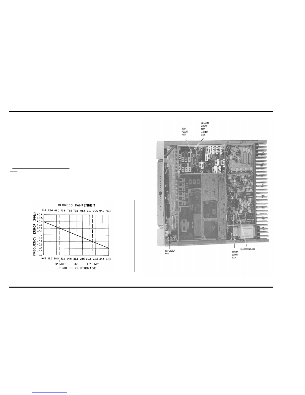
Figure 9 - Frequency Characteristics Vs. Temperature . . . . . . . . . . . . . . . . . . . . . . . . . . . . . . . . . 6
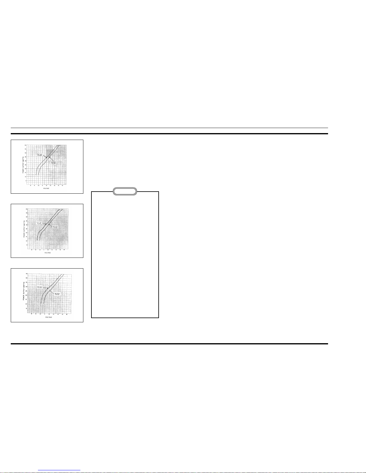
Figure 10 - 40-Watt Power Output Setting Chart . . . . . . . . . . . . . . . . . . . . . . . . . . . . . . . . . . . . 8
Figure 11 - 38-Watt Power Output Setting Chart . . . . . . . . . . . . . . . . . . . . . . . . . . . . . . . . . . . . 8
Figure 12 - 35-Watt Power Output Setting Chart . . . . . . . . . . . . . . . . . . . . . . . . . . . . . . . . . . . . 8
SPECIFICATIONS *
Power Output
406-420 MHz & 450-470 MHz 40 Watts (A djusta ble fr om 1 2 t o 40 Watts)
470-494 MHz 38 Watts (Adjustable fr om 12 to 38 Watts)
494-512 MHz 35 Watts (Adjustable fr om 12 to 35 Watts)
Crystal Multiplication Factor 36
Frequency Stability
5C-ICOM with EC-ICOM ±0.0005% (-40°C to +70°C)
5C-ICOM or EC-ICOM ±0.0002% (0°C to +55°C)
2C-ICOMS ±0.0002% (-40°C to +70°C)
Spurious and Harmonic Emission At least 80 dB below full rated power output.
Modulation Adjustable from 0 to ±5 kHz swing with instantaneous
modulation limiting.
Modulation Sensitivity 75 to 120 Millivolts
Audio Frequency Characteristics Within +1 dB to -3 dB of a 6-dB/octave pre-emphasis from
300 to 3000 Hz per EIA standards. Post limiter filter per FCC
and EIA.
Distortion Less than 2% (1000 Hz)
Less than 3% (300 to 3000 Hz)
Deviation Symmetry 0.5 kHz maximum
Maximum Frequency Spread (2 to 8 channels) Full Specifications 1 dB Degradation
406-420 MHz 2.75 MHz 6.00 MHz
450-470 MHz 2.75 MHz 9.00 MHz
470-494 MHz 2.90 MHz 9.50 MHz
494-512 MHz 3.00 MHz 9.75 MHz
Duty Cycle EIA 20% Intermitt en t
RF Output Impedance 50 Ohms
* These specifications are inte nd ed p rimarily for the use of the serviceman. Refer to the appropriate S p ec if ic at i o n S heet for the
complete specifications.
Although the highest DC voltage in MASTR II Mobile Equipment is supplied by the vehicle battery, high currents
may be drawn under short circuit conditions. These currents can possibly heat metal objects such as tools, rings,
watchbands, etc., enough to cause burns. Be careful when working near energized circuits! High-level RF energy in
the transmitter Power Amplifier assembly can cause RF burns upon contact. KEEP AWAY FROM THESE CIRCUITS WHEN THE TRANSMITTER IS ENERGIZED!
W ARNING
LBI-4622 LBI-4622
1
Page 3
DESCRIPTION
MASTR II transmitters are crystal controlled, phase
modulated transmitters designed for one through eight-frequency operation in the 406 to 420 and 450 to 512 megahertz band. The solid state transmitter utilizes both
integrated circuits (ICs) and discrete components, and consists of the following assemblies:
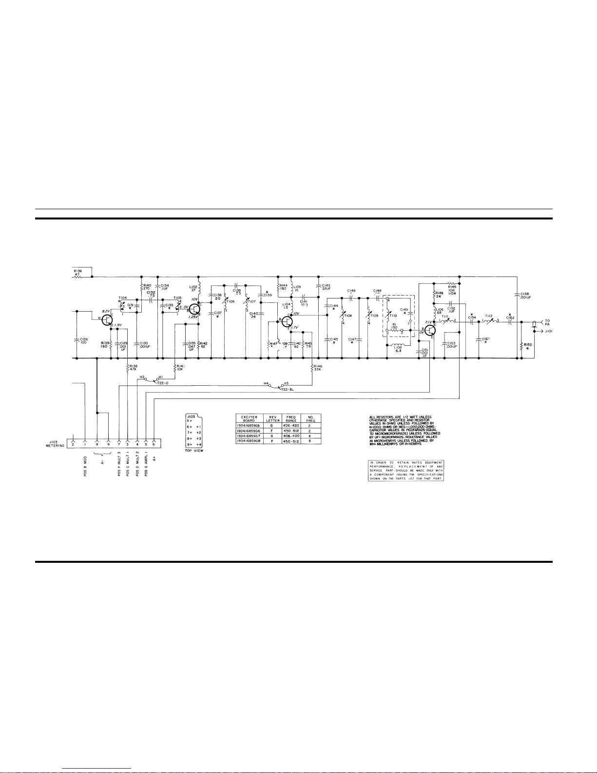
Exciter Board; with audio, modulator, amplifier and mul-
tiplier stages
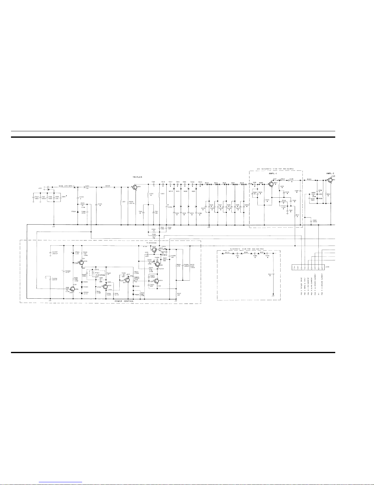
Power Amplifier Asse mbly; with amplifier, driver, PA,
power control, filter and antenna switch.
CIRCUIT A NALYSIS
EXCITER
The exciter uses seven transistors and one integrated circuit to drive the PA assembly. The exciter can be equipped
with up to eight Integrated Circuit Oscillator Modules
(ICOMs). The ICOM crystal frequency ranges from approximately 11.3 to 14.2 megahertz, and the crystal frequency is multiplied 36 times.
Audio, supply voltages and control functions are connected from the system board to the exciter board through
P902.
Centralized metering jack J103 is provided fro use with
GE Test Set Model 4EX3A11 or Test Kit 4EX8K12. The
test set meters the modulator, multiplier and amplifier stages,
and the regulated 10-Volts.
ICOMS
Three different types of ICOMs are available for use in
the exciter. Each of the ICOMs contains a crystal-controlled
Colpitts oscillator, and two of the ICOMs contain compensator ICs. The different ICOMs are:
5C-ICOM - contains an oscillator and a 5 part-per-mil-
lion (±0.0005%) compensator IC, Provides compensa-
tion for EC-ICOMs.
EC-ICOM - contains an oscillator only. Requires exter-
nal compensation from a 5C-ICOM.
2C-ICOM - contains an oscillator only. 2 PPM
(±0.0002%) compensator IC. Will not provide compen-
sation for an EC-ICOM.
The ICOMs are enclosed in an RF shielded can with the
type ICOM (5C-ICOM, EC-ICOM or 2C-ICOM) printed on
the top of the can. Access to the oscillator trimmer is obtained by prying up the plastic tab on the t op of the can. The
tabs can also be used to pull the ICOMs out of t he radio.
Frequency selection is accomplished by switching the
ICOM keying lead (terminal 6) to A- by means of the fre-
quency select or switch on the control unit. In single-frequency radios, a jumper from H9 to H10 in the control unit
connects terminal 6 of the ICOM to A-. The oscillator is
turned on by applying a keyed +10 Volts to the external oscillator load resistor.
In Standard 5 PPM radios using EX-ICOMs, at least one
5C-ICOM must be used. The 5C-ICOM is normally used in
the receiver Fl position, but can be used in any transmit or receive position. One 5C-ICOM can provide compensation for
up to 15 EC-ICOMs in the transmit and receiver. Should the
5C-ICOM compensator fail in the open mode, the EC-ICOMs
will still maintain 2 PPM frequency stability from 0°C to 55°C
(+32°F to 131°F) due to the regulated compensation voltage (5
Volt s) from the l0-Vo lt regulator IC. If desired, up to 16 SCICOMs may be used in the radio.
The 2C-ICOMs are self-compensated at 2 PPM and will
not provide compensation for EC-ICOMs.
Oscillator Circuit
The quartz crystals used in ICOMs exhibit the traditional
"S" curve characteristics of output frequency versus operating
temperature.
At both the coldest and hottest temperatures, the frequency
increases with increasing temperature. In the middle temperature range (approximately 0°C to 55°C), frequency decreases
with increasing temperature.
Since the rate of change is nearly linear over the mid-temperature range, the output frequency change can be compensated by choosing a parallel compensation capacitor with a
temperature coefficient approximately equal and opposite that
of the crystal.
Figure 2 shows the typical performance of an uncompensated crystal as well as the typical performance of a crystal
which has been matched with a properly chosen compensation
capacitor.
At temperatures above and below the mid-range, additional
compensation must he introduced. An externally generated
compensation voltage is applied to a varactor (voltage-variable
capacitor)which is in parallel with the crystal.
A constant bias of 5 Volts (provided from Regulator IC
U901 in parallel with the compensator) establishes the varactor
capacity at a constant value over the entire mid-temperature
range. With no additional compensation, all of the oscillators
will provide 2 PPM frequency stability from 0°C to 55°C
(+32°F to 131°F).
Compensator Circuits
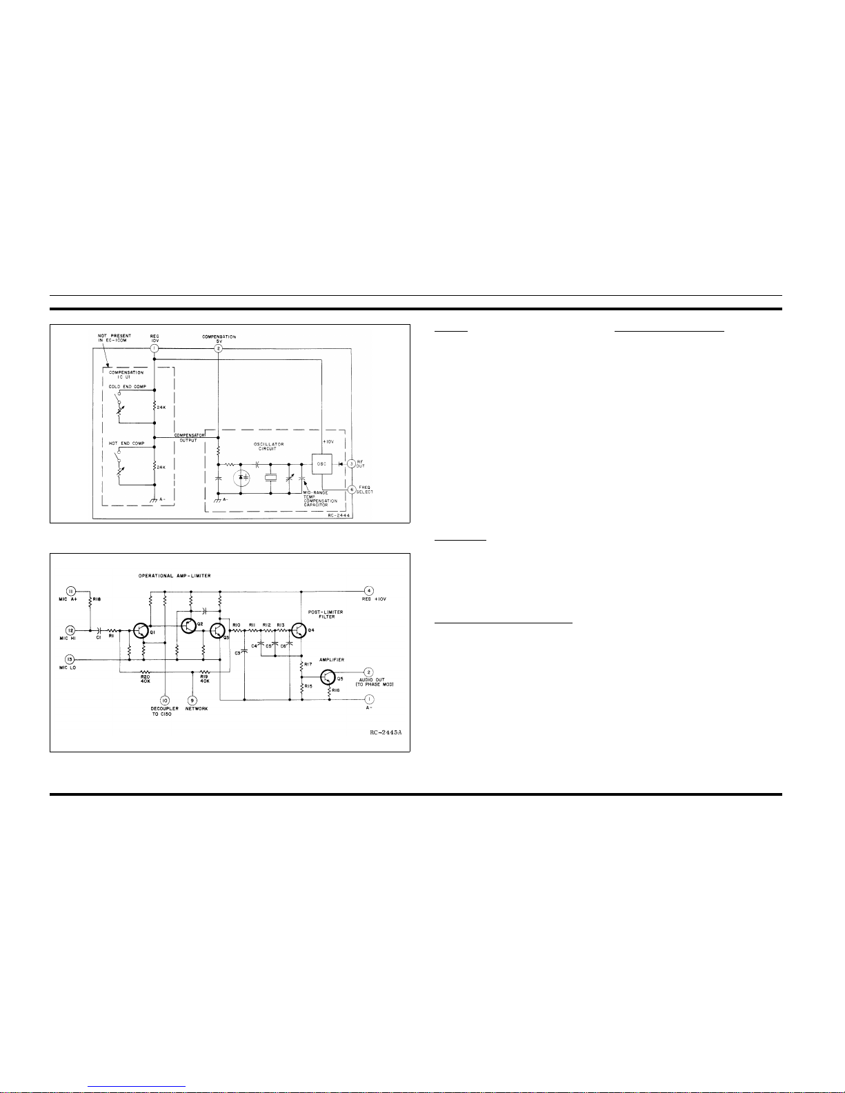
Both the SC-ICOMs and 2C-ICOMs are temperature compensated at both ends of the temperature range to provide instant frequency compensation. An equivalent ICOM circuit is
shown in Figure 3.
The cold end compensation circuit does not operate at temperatures above 0°C. When the temperature drops below 0°C,
the circuit is activated. As the temperature decreases , the
equivalent resistance decreases and the compensation voltage
increases.
The increase in compensation voltage decreases the capacity of the varactor in the oscillator, increasing the output frequency of the ICOM.
The hot end compensation circuit does not operate at temperatures below +55°C. When the temperature rises above
+55°C, the circuit is activated, As the temperature increases,
the equivalent resistance decreases and the compensation voltage decreases. The decrease in compensation voltage increases
the capacity of the varactor, decreasing the output frequency of
the ICOM.
SERVICE N OTE: Proper ICOM operation is dependent on
the closely-controlled input voltages from the 10-Volt
regulator. Should all of the ICOMs shift off frequency, check
the 10- Volt regulator module.
Figure 1 - Transmitter Block Diagram
All ICOMs are individually compensated at the factory
and cannot be repaired in the field. Any attempt to repair or change an ICOM frequency will void the warranty.
CAUTION
Figure 2 - Typical Crystal Characteristics
LBI-4622 LBI-4622
2
Page 4
Audio IC
The transmitter audio circuitry is contained in audio IC
U101. A simplified drawing of the audio IC is shown in Figure 4.
Audio from the microphone at pin 12 is coupled through
pre-emphasis capa citor C1 to the bas e of Q1 in the operational amplifier-limiter circuit. Collector voltage for the
transistorized microphone preamplifier is supplied from pin
11 through microphone collector load resistor R18 to pin 12.
The operational amplifier-limiter circuit consists of Q1,
Q2 and Q3. Q3 provides limiting at high signal levels. The
gain of the operationa l ampli fier circ uit is fixed by negative
feedback through R19, R20 and the resistance in the n etwork
(Pin 9).
The output of Q3 is coupled through a de-emphasis network (R10 and C3) to an active post-limiter filter consisting
of C4, C5, C6, R11 , R12, R13, R15, R17 and Q4 .
Following the post-limiter filter is class A amplifier Q5.
The output of Q5 is coupled through MOD ADJUST potentiometer R104 and resistor R125 to the phase modulator.
SERVICE NOTE: If the DC voltages to the Audio IC are
correct and no audio output can be obtained, replace U101.
For radios equipped with Channel Guard, tone from the
encoder is applied to the phase modulator through CHANNEL GUARD MOD ADJUST potentiometer R105, and resistor R127. Instructions for setting R105 are contained in
the modulation adjustment section of the Transmitter Alignment Procedure.
Buffer, P hase Modulators & Amplifiers
The output at pin 3 of the selected ICOM is coupled
through buffer-amplifier Q101 to the modulator stage. The
phase modulator is varactor (voltage-variable capacitor)
CV103 in series with tunable coil T103. This network appears as a series-resonant circuit to the RF output of the oscillator. An audio signal applied to the modulator circuit
through blocking capacitor C107 varies the bias of CV103,
resulting in a phase modulated output. A voltage divider
network (R110 and R111) provides the proper bias for var actor CV103.
The output of the modulator is coupled through blocking
capacitor C150 to the base of Class A amplifier Q104. The
output of the modulator is metered through C123, R128 and
CR104, and is applied to the base of buffer Q105. Diodes
CR105 and CR106 remove any amplitude modulation in the
modulator output.
Buffer, Multipliers & Amplifier
Buffer Q105 is saturated when no RF signal is present,
Applying an RF signal to Q1O5 provides a sawtooth waveform at its collector to drive the class C tripler, Q106. The
tripler stage is metered through R138, The output of Q106 is
coupled through tuned circuits T104 and T105 to the base of
doubler Q107. The doubler stage is metered through R141.
The output of Q107 is coupled through tuned circuits
T106 and T107 to the base of second doubler Q108. Q108
is metered through R146
The output of Q108 is coupled through three tuned circuits (T108, T109 and T110) to the base of amplifier Q109.
Q109 is a Class C amplifier, and is metered through
R148. The amplifier collector circuit consists of T111,
C154, C155, T112 and C157, and matches the amplifier output to the input of the power amplifier assembly.
POWER AMPLIFIER
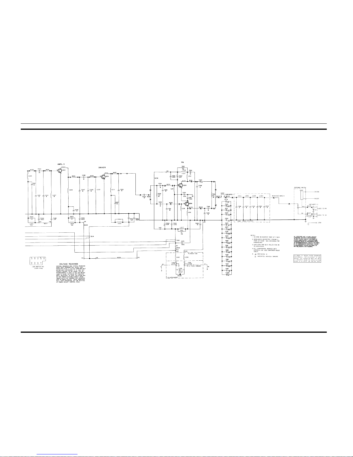
The PA assembly uses seven RF power transistors and
seven transistors in the Power Control circuitry to provide
rated power output. The broadband PA has no adjustments
other than Power Control potentiometer R226.
Supply voltage for the pA is connected through power
leads from the system board to feed through capacitors C297
and C298 on the bottom of the PA assembly, C297, C298,
C299, L295 and L296 prevent RF from getting on the power
leads. Diode CR295 will cause the main fuse in the fuse assembly to blow if the polarity of the power leads is reversed,
providing reverse voltage protection for the radio.
Centralized metering jack J205 is provided for use with
GE Test Set Model 4EX3A11 or Test Kit 4EX8K12. The
Test Set met ers t h e Tripler drive (exciter output), A mp1-2 input, Driver and PA current.
TRIPLER & RF AMPLIFIERS
The exciter output is coupled through an RF cable to PA
input jack J201. The 50-ohm RF input is coupled through a
matching network (C206 and w209) to the base of the broadband tripler stage, Q201.
Part of the RF input is rectified by CR201 and is used to
activate the Power Control circuit. Another portion of the
rectified RF is applied to J205 for metering the tripler drive.
Figure 3 - Equivalent ICOM Circuit
Figure 4 - Sim pl i fi e d A udio IC
LBI-4622 LBI-4622
3
Page 5
The output of Q201 is coup led through a 20-ohm collector matching network (C212, C213, C4219 and L203) to the
input of a high-pass filter consisting of C217 through C225,
and w210 through w213.
Following the high-pass filter is a low-pass filter consisting of w214 through w219, C226 through C230 (and C4214
through C4217 in the 406-420 MHz band). The two filter
sections combine to act as a bandpass filter providing a
minimum of 60 dB rejection below 300 megahertz and 30
dB rejection above 600 megahertz.
In 450 to 512 megahertz transmitters, the filter output is
coupled through a matching network (C231, C232, C233
and w220) to the base of Class C amplifier Q207. Collector
voltage to Q207 is coupled through collector stabilizing network L220, R216 L219 and C234. The output of Q207 is
coupled through a matching network (w221, C236, C237
and w222) to the base of the second Class C a mplifier Q202.
Drive to Q202 is metered at J205 (Amp1-2 Input) through
metering network C238, CR202, C239 and R205.
In 406 to 420 megahertz transmitters, Q207 and its associated circuitry is removed, and the filter output is coupled
through C285 to the base of second amplifier Q202,
Collector voltage for Q202 is coupled through stabilizing
network L206, R206, L205 and C240. Matching network
w223,C241, C242, C243 and W224 matches the output of
Q202 to the base of third amplifier Q203.
Collector voltage for Q203 is applied through stabilizing
network R207, L209, and C246.
The output of Q203 is coupled through a matching network (w225, C247, C248, C249 and w226) to the base of
Class C driver Q204. Collector voltage for Q204 is applied
through collector stabilizing network C201, L211 and C267.
Collector current for Q204 is metered across tapped
manganin resistor R214 at J205 (Driver Current). The reading is taken on the one-Volt scale with the High Sensitivity
button pressed, and read as 10 amperes full scale.
Following Q204 is a matching network (w227 and C253)
that matches the driver output to the 50-ohm impedance of
power divider network W228 and R209.
The power amplifier stages consist of two identical paralleled Class C PA circuits (Q205 and Q206). One output of
the power divider network is applied to the bas e of Q205
through matching network W229 and C268
Supply voltage for Q205 is coupled through collector
stabilizing network L213, R210, L214 and C255. The output of Q205 is coupled through a matching network (W231
and C258) and added to the output of Q206 in power combiner network R212 and W233. The combined collector current for Q205 and Q206 is metered across tapped manganin
resistor R213 at J205 (PA Current). The reading is taken on
the one-Volt scale with the High Sensitivity button pressed,
and read as 10 amperes full scale.
The PA output is coupled through a low-pass filter to the
antenna through antenna switch K201. Capacitors C214,
C270 through C4218 provide DC ground isolation for ±
ground operation.
POWER CONTROL CIRCUIT
When the transmitter is keyed, rectified RF from CR201
is applied to the base of switch Q208, turning it on. Turning
on Q208 turns on voltage regulator Q210, supplying a constant voltage to Power Adjust potentiometer R226.
Q212, Q213 and Q215 operate as an amplifier chain to
supply voltage to the collector of Q202 (Amp1-2). The setting of R226 determines the voltage applied to the base of
Q212. The higher the voltage at the base of Q212, the
harder the amplifiers conduct, supplying more collector voltage to Q202. The lower the voltage at the base of Q212, the
less collector voltage is supplied to Q202. Reducing the
supply voltage to Q202 reduces the drive to Q203 and Q204,
thereby reducing the power output of the PA. The power
output can be adjusted by R226 from approximately 12 to 40
Watts.
Temperature protection is provided by Q209, Q211 and
thermistor RT201 which is mounted in the PA heatsink. Under normal operating conditions, the circuit is inactive
(Q209 is on and Q211 is off). When the heatsink temperature reaches approximately 100°C, the resistance of RT201
decreases. This increases the base voltage applied to Q209,
turning it off. Turning off Q209 allows Q211 to turn on, decreasing the voltage at Power Adjust potentiometer R226.
This reduces the base voltage to Q212 which causes Q213
and Q215 to conduct less, reducing the collector voltage to
Q202 (Amp1-2) . This reduces the transmitter output power,
keeping the heatsink at a maximum of approximately 100°C.
When the heatsink temperature decreases below 100°C, the
temperature control circuit turns off, allowing the normal transmitter power output.
CARRIER CONTROL TIMER
The Carrier Control Timer option shuts off the transmitter
on each transmission after a one-minute timing cycle, and
alerts the operator that the transmitter is off by means of an
alarm tone in the speaker. The transmitter can be turned on
again by releasing and rekeying the push-to-talk switch on the
microphone.
The timing cycle (transmitter keyed time) is normally set at
the factory for a duration of one minute. A potentiometer permits the timing cycle to be adjusted from approximately 15
second to 3 minut es .
MAINTENANCE
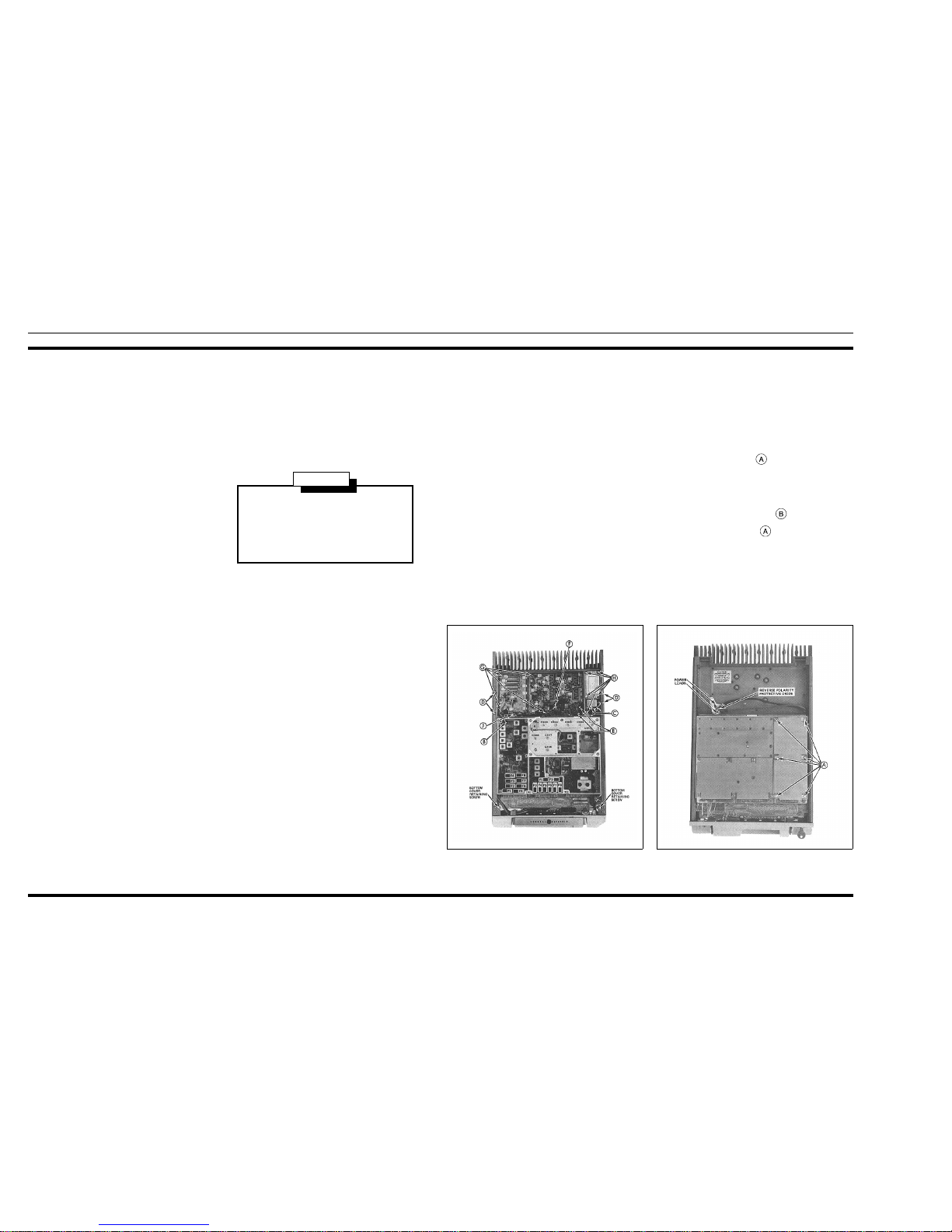
DISASSEMBLY
To service the transmitter from the top:
1. Pull the locking handle down, then pry up the c o ve r a t
the front notch and lift off the cover.
To service the tra nsmit te r from the bott om:
1. Pull the locking handle down and pull the radio out of
the mounting frame.
2. Remove the top cover, then loosen the two bottom
cover remaining screw s and re move t he bot tom co ver
(see Figure 5).
3. To gain access to the bottom of the exciter board, remove the six screws holding the exciter board
and its bottom cover to the module mounting frame,
and remove the bottom cover.
To remove the exciter board from the radio:
1. Unplug the exciter/PA cable
2. Remove the six screws holding the exciter board
and its bottom cover to the module mounting frame
(see Figure 6).
3. Press straight down on the plug-in exciter from the
top to avoid bending the pins when unplugging the
board from the system board jack.
The stud mount RF Power Transistors used in the
transmitter contain Beryllium Oxide, a TOXIC Substance. If the ceramic, or other encapsulation is
opened, crushed, broken or abraded, the dust may be
hazardous if inhaled. Use care in replacing transistors of this type.
W ARNIN G
Figure 5 - Disassembly Procedure Top View Figure 6 - Disassembly Procedure Bottom View
LBI-4622 LBI-4622
4
Page 6
To remove the PA assembly:
1. Remove the PA top cover and unplug the exciter/PA
cable , the antenna, receiver and PTT cables
2. Remove the four side-rail screws , and unsolder
the power cables from the bottom of the PA assembly
if desired.
To remove the PA board:
1. Remove the PA top cover and unplug the exciter/PA
cable
2. Unsolder the two feed through coils and the thermistor leads
3. Remove the PA transistor hold-down nuts and spring
washers on the bottom of the PA assembly.
4. Remove the four PA board mounding screws , the
five screws in the filter casting , and the retaining
screw in Q215 , and lift the board o u t.
PA TRANSISTOR REPLACEMENT
To replace the PA RF transistors:
1. Unsolder one lead at a time with a 50-Watt soldering
iron. Use a scribe to hold the lead away from the
printed circuit board until the solder cools.
2. Turn the transmitter over.
3. Hold the body of the transistor to prevent it from tu r ning. Remove the transistor hold-down nut and spring
washer through the hole in the heats ink with am
11/32-inch nut-driver. Lift out the transistor, and remove the old solder. from the printed circuit board
with a de-soldering tool such as a SOLDA PULLT®.
Special care should be taken to prevent damage to the
printed circuit board runs because part of the matching network is included in the base and collector runs.
4. Trim the new transistor leads (if required) to the lead
length of the removed transistor. Cut the collector
lead at a 45° angle for future identification (see Figure
7). The letter "C" on the top of the transistor also indicates the collector.
5. Applying a coating of silicon grease around the transistor mounting surface, and place the transistor in the
mounting hole. Align the leads as shown in the Outline Diagram. Then hold the body of the transistor
and replace the holding-down nut and spring-washer,
using moderate torque (8 inch-pounds). A torque
wrench must be used for this adjustment since transis tor damage can result if too little or too much torque
is used.
6. Make sure that the transistor leads are formed as
shown in Figure 8 so that the leads can be soldered to
the printed circuit pattern, starting from the i nner edg e
of the mounting hole.
7. Solder the leads to the printed circuit pattern. Start at
the inner edge of mounting hole and solder the remaining length of transistor lead to the board. Use
care not to use excessive heat that causes the
printed wire board runs to lift up from the board.
Check for shorts and solder bridges before applying
power.
MODULATION LEVEL ADJUSTMENT
The MOD ADJUST (R104) was adjusted to the proper
setting before shipment and should not normally require readjustment. This setting permits approximately 75% modulation for the average voice level. The audio peaks which
would cause overmodulation are clipped by the modulation
limiter. The limiter, in conjunction with the de-emphasis
network, instantaneously limits the slope of the audio wave
to the modulator, thereby preventing overmodulation while
preserving intelligibility.
TEST EQUIPMENT
l. An audio oscillator (GE Model 4EX6A10)
2. A frequency modulation monitor
3. An output meter or a VTVM
4. GE Test Set Model 4EX3A11 or 4EX8K12
PROCEDURE
l. Connect the audio oscillator and the meter across
audio input terminals J10 (Green-Hi) and J11
(Black-Lo) on GE Test Set, and connect red Test
Set plug to the System red metering plug. If not using GE Test Set, connect audio oscillator and meter
across P902-6 (Mike High) through a 0.5 microfarad (or larger) DC blocking capacitor, and P902-5
(Mike- Low) on the System Board
2. Adjust the audio oscillator for 1-Volt RMS at 1000
Mz.
3. For transmitters without Channel Guard, set MOD
ADJUST R104 for a 4.5-kHz swing with the devia tion polarity which gives the highest reading as indicated on the frequency modulation monitor.
4. For transmitters with Channel Guard, set Channel
Guard MOD ADJUST R105 for zero tone deviation. Next, with the l-Volt signal at 1000 Hz applied, set MOD ADJUST R104 for 3.75 kHz
deviation. Then remove the signal from the audio
oscillator and set Channel Guard MOD ADJUST
R105 for 0.75 kHz to n e deviation.
5. For multi-frequency transmitters, set the deviation
as described in Steps 3 or 4 on the channel producing the largest amount of deviation.
PA POWER INPUT
For FCC purposes, the PA power input can be determined by measuring the PA supply voltage and PA current,
and using the following formula:
P
i
= PA voltage x PA current
where:
P
i
is the power input in Watts,
PA voltage is measured with Test Set Mod el 4EX3A11 in
Position G on the 15-Volt range (read as 15 Volts full
scale), and with the polarity switch in the (-) position.
With Test Set Model 4EX8K12, use the H+ position and
the l-Volt range (read as 15 Volts full scale), with the
HIGH SENSIT IVITY button pressed and t he polarity
switch in the (-) position.
PA current is measured with the Test Set in Position G in
the Test l position, and with the HIGH SENSITIVITY
button pressed (10 amperes full scale)
Example:
P
i
= 12.6 Volts x 3.4 amperes = 43 Watts
ICOM FREQUENCY ADJUSTMENT
First, check the frequency to determine if any ad justmen t
is required. The frequency should he set with a frequency
meter or counter with an absolute accuracy that is 5 to 10
times better than the tolerance to be maintained, a nd with the
entire radio as near as possible to an ambient temperature of
26.5°C (79.8°F)
The stud mount RF Power Transistors used in the
transmitter contain Beryllium Oxide, a TOXIC Substance. If the ceramic, or other encapsulation is
opened, crushed, broken or abraded, the dust may be
hazardous if inhaled. Use care in replacing transistors
of this type.
WARNING
Figure 7 - Le ad Identification
Figure 8 - Le ad Forming
Failure to solder the transistor leads as directed may
result in the generation of RF loops that could damage the transistor or may caus e low power output.
CAUTION
LBI-4622 LBI-4622
5
Page 7
MASTR II ICOMs should be reset only when the fre-
quency shows deviation in excess of th e follow ing l im its:
A. ±0.5 PPM, when the radio is at 26.5°C (79.8°F).
B. ±2 PPM at any other temperature within the range
of -5°C to +55°C (+23°F to + 13 1°F )
C. The specification limit (±2 PPM or +5 PPM) at any
temperature within the ranges of -40°C to -5°C (40°F to +23°F) or +55°C to +70°C (+131°F to
+158°F)
If an adjustment is required, pry up the cover on the top
of the ICOM to expose the trimmer, and use one of the following procedures
If the radio is at an ambient temperature of 26.5°C
(
79.8°F), set the oscillator for the correct operating fre-
quency.
If the radio is not at an ambient temperature of 26.5°C
setting errors can be minimized as follows:
A. To hold the setting error to ±0.6 PPM (which is
considered reasonable for 5 PPM ICOMS):
l. Maintain the radio at 26.5°C (±5°C) and set the
oscillator to desired frequency, or
2. Maintain the radio at 26.5°C (±10°C) and off-
set the oscillator, as a function of actual temperature, by the amount shown in Figure 9.
B. To hold setting error to +0.35 PPM (which is con-
sidered reasonable for 2 PPM ICOMs) Maintain
unit at 26.5°C (+5°C) and offset the oscillator as a
function of actual temperature, by the amount
shown in Figure 9.
For example: Assume th e ambient temperature of the radio
is 18.5°C (65.4°F). At that temperature, the curve shows a
correction factor of 0.3 PPM. (At 406 MHz, 1 PPM is 406
Hz. At 512 MHz, 1 PPM is 512 Hx).
With an operating frequency of 450 MHz, set the oscillator for a reading of 135 Hz (0.3 x 450 Hz) higher than the licensed operating frequency. If a negative correction f actor is
obtained (at temperatures above 26.5°C), set the oscillator
for the indicated PPM lower than the licensed operating frequency.
Figure 9 - Frequency Characteristics Vs. Temper at ur e
LBI-4622 LBI-4622
6
Page 8
TRANSMITTER ALIGNMENT
EQUIPMENT REQUIRED
1. GE Test Set Model 4EX3A11 or Test Kit 4EX8K12.
2. A 50-ohm wattmeter conn ecte d to antenna jack J906.
3. A frequency counter.
PRELIMINARY CHECKS AND ADJUSTMENTS
1. Place ICOMs on Exciter Board (crystal frequency = operating frequency 36).
2. For a large change in frequency or badly mis-aligned transmitter, pre-set the slugs in T104 and T105 to the bottom of the
coil form. Pre-set all of the other slugs to the top o f the c oi l fo rm.
3. For multi-frequency transmitters with a frequency spread less than that specified in column (1) tune the transmitters to the
lowest frequency. For a frequency spread exceeding the limits specified in column (1) tune the transmitters u sing a center
frequency tune up ICOM. Except the maximum frequency spread can be extended to the limits specified in column (3)
with l dB degradation.
For tuning L101, L102, and L103, always tune L101, L1O2, a nd L1O3 on the lowest frequency.
Multi-frequency Transmitter Tuning
TRANSMITTER
FREQUENCY RANGE
MAXIMUM FREQUENCY SPREAD
(1) Without center tuning With center tuning W i t h cente r tuning (1 dB degradation )
406-420 MHz
450-470 MHz
470-494 MHz
494-512 MHz
2.75 MHz
2.75 MHz
2.90 MHz
3.00 MHz
5.50 MHz
5.50 MHz
5.80 MHz
6.00 MHz
6.00 MHz
9.00 MHz
9.50 MHz
9.75 MHz
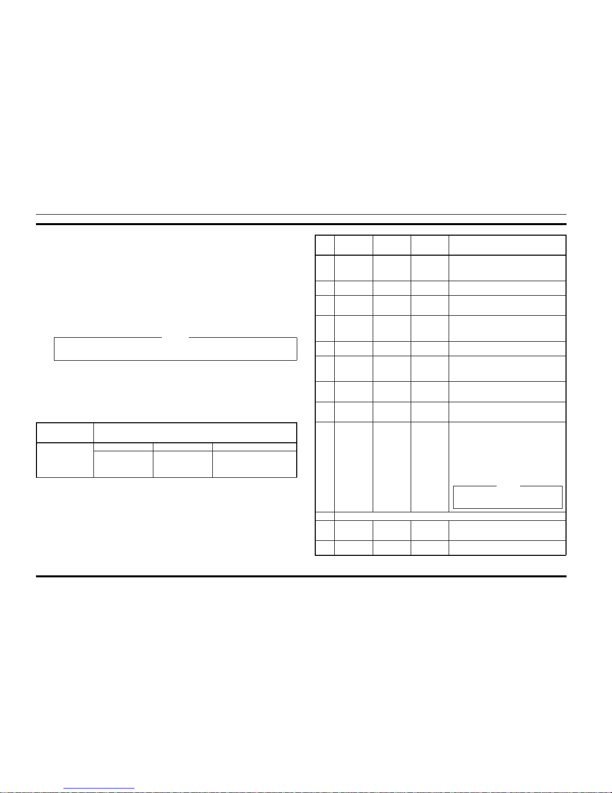
4. Connect the red plug on the GE Test Set to the System Board metering jack, and the black plug to the Exciter metering
jack. Set the polarity to +, and set the range to the Test 1 position (l-Volt position for 4EXBK12) for all adjustments.
NOTE: With the Test Set connected to the PA metering jack, the voltage reading at position "F" with the HIGH SENSITIVITY button pressed may be converted to driver collector current by reading the current as 10 amperes full scale. The
voltage reading at position "G" with the HIGH SENSITIVITY button pressed may be converted to PA collector current by
reading the current as 10 amperes full scale.
5. All adjustments are made with the transmitter keyed. Unkey the transmi tte r between steps to avoid unnecessary heating.
The tuning frequency for multi-frequency transmitters is determined by the operating frequency and the frequency
spread between transmitters. Refer to the table below for maximu m fr equency sprea d.
NOTE
STEP METER
POSITION
TUNING
CONTROL
METER
READING
PROCEDURE
1. B
(MOD-1)
T103 See Procedure Tune T103 for the m aximum meter reading on the
lowest frequency, After tuning T103 for maximum,
turn the slug 1/8 of a turn clockwise (increasing
inductance).
2. C
(MULT-1)
T104 Minimum Tune T104 for a dip i n m ete r reading.
3. D
(MULT-2)
T105, T104
& T106
See procedure Tune T105 for maximum met er r e ad ing a nd re-adjust
T104 for maximum meter reading. Then tune T106 for
a dip in meter reading.
4. F
(MULT-3)
T107, T106,
T108 & T109
See procedure Tune T107 for maximum met er r e ad ing a nd re-adjust
T106 for maximum meter reading. Then tune T108 for
a dip in meter reading and T 109 for maximum meter
reading.
5. G
(AMPL-1)
T110, T108 Maximum Tune T110 for maximum meter reading. and then re-
adjust T108 and T109 for maximum me t er r ead ing.
6. D
(AMPL-1 DRIVE
on pA)
T111 & T11 2 Maximum Move the black detering plug to the power Amplifier
metering jack and tune T111 and then T112 for
maximum meter reading. Then alternately tune T111
and T112 for maximum meter reading.
7. G
(AMPL-1)
T108, T109
& T110
Maximum Move the black metering plug hack to the exciter meter
ing jack and re-adjust T 1 08 , T 109 a nd T 110 for
maximum meter reading.
8. D
(AMPL-1 DRIVE
on PA)
T111 & T11 2 Maximum Move the black metering plug back to the Power
Amplifier metering jack and re-adjust Till and T112 for
maximum meter reading.
9. R226 With tire battery v o lt ag e a t 13.6 volts or the PA
collector voltage at 13.0 volts, set Power Adjust
potentiometer R226 on the PA hoard for the desired
power output (from 12 to 40 Watts).
If the battery volta ge i s n ot a t 13 .6 volts or the
collector voltage at 13.0 volts and full rated outputs
desired (40,38 or 35 Watts at 13.6 volts), set R226 for
the output power according to tie battery voltage or
collector voltage shown in Figures 10, 11 or 12.
ADDITIONAL STEPS FOR TRANSMITTERS USING CENTER FREQUENCY TUNE-U P ICOM
10. D
(MULT-2)
T105 See procedure Move the black metering plug to the exciter metering
jack and re-adjust T105 for equal drive on the highest
and lowest frequency.
11. G
(AMPL-1)
T110 & T108 Maximum Re-adjust T110 and then T108 for maximum meter
reading on the lowest frequency.
The PA collector voltage is measured as described
in the PA POWER INPUT section.
NOTE
LBI-4622 LBI-4622
7
Page 9
TEST PROCEDURES
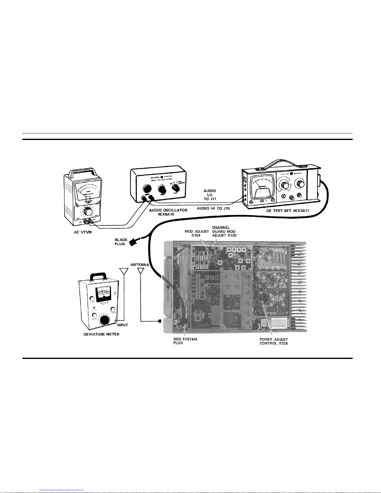
These Test Procedures are designed to assist you in servicing a transmitter that is operating-- but not properly. Problems encountered could be low power output, tone and voice
deviation, defective audio sensitivity, and modulator adjust
control set too high. Once a defect is pin-pointed, refer to
the "Service Check" and the additional corrective measures
included in the Transmitter Troubleshooting Procedure. Before starting with the Transmitter Test Procedures, be sure
the transmitter is tuned and aligned to the proper operating
frequency.
TEST EQUIPMENT REQUIRED
for test hookup as shown:
l. Wattmeter similar to:
Bird # 43
Jones # 711N
2. VTVM similar to:
Triplett # 850
Heath # IM-21
3. Audio Generator similar to:
GE Model 4EX6A10
4. Deviation Meter (with a .75 kHz scale) similar to:
Measurements # 720
5. Multimeter similar to:
GE TEST SET MODEL 4EX3A11,
MODEL 4EX8K12 or
20,000 ohms-per- Volt voltmeter
POWER MEASUREMENT
TEST PROCEDURE
1. Connect transmitter output from the antenna jack to
the wattmeter through a 50-ohm coaxial cable. Make
sure the wattmeter is terminated into a 50-ohm load.
2. Key the transmitter and check the wattmeter for the
desired power output.
SERVICE CHECK
Check the setting of the Power Adjust Control (R226).
Refer to the QUICK CHECKS on the Transmitter Troubleshooting Procedure.
VOICE DEVIA TION SYMMETRY AND
AUDIO SENSITIVITY
TEST PROCEDURE
l. Connect the test equipment to the transmitter as
shown.
2. In radios with Channel Guard, set Channel Guard
Mod Adjust R105 for zero tone deviation.
3. Set the Audio generator output to 1.0 VOLTS RMS
and frequency to 1 kHz.
4. Key the transmitter and adjust Deviat ion Meter to carrier frequency.
5. Deviation leading should be ±4.5 kHz in radios without Channel Guard, and ±3.75 kHz in radios with
Channel Guard.
6. If necessary, adjust MOD ADJUST control R104 for
the proper deviation on plus (+) or minus (-) deviation, whichever is greater.
NOTES:
MASTR II transmitters are adjusted for 4.5 kHz deviation
at the factory . The factory adjustment will prevent the
transmitter from deviating more than 5.0 kHz under the
worst conditions of frequency, voltage and temperature.
7. If the deviation reading plus (+) or minus (-) differs
by more than 0.5 kHz, recheck Steps 1 and 2 as
shown in the Transmitter Alignment Char t.
8. Check Audio Sensitivity by reducing generator output
until deviation falls to 3.0 kHz for radios without
Channel Guard, or 2.25 kHz for radios with Channel
Guard. Voltage should be LESS than 120 millivolts.
If not, refer to the Transmitter Troubleshooting Procedure.
TONE DEVI ATIO N WITH CHANNEL
GUARD TEST PROCEDURE
TEST PROCEDURE
1. Set up the Deviation Meter and monitor the output of
the transmitter.
2. Remove the 1000 Hz signal from the audio generator.
3. Key the transmitter and check for 0.75 kHz deviation.
If the reading is low or high, adjust Channel Guard
MOD ADJUST R105 for a reading of 0.75 kHz.
NOTES:
1. On units supplied with Channel Guard, the Phase
Modulator Tuning should be adjusted Carefully to insure proper performance. (Refer to Step 1 in the
Transmitter Alignment Chart).
2. The Tone Deviation Test Procedures should be repeated every time the Tone Frequency is changed.
Figure 10 - 40-Watt Power Output Setting Chart
Figure 11 - 38-Watt Power Output Setting Chart
Figure 12 - 35-Watt Power Output Setting Chart
Before bench testing the MASTR II Mobile Radio,
be sure of the output voltage characteristics of your
bench power supply.
To protect the transmitter power output transistors
from possible instant destruction, the following input voltages must not b e exc eeded:
Transmitter unkeyed: 20 Volts
Transmitter keyed (50 ohm resistive load): 18
Volts
Transmitter keyed (no load or non-resistive load):
15.5 Volts
These voltages are specified at the normal vehicle
battery terminals of the radio and take the voltage
drop of standard cables into account. The voltage
limits shown for a non-optimum load is for "worst
case" conditions. For antenna mis- matches likely to
be encountered in practice, the actual limit will approach the 18 V olt figure.
Routine transmitter tests should be performed at EIA
Standard Test Voltages (13.6 VDC for loads of 6 to
16 amperes: 13.4 VDC for loads of 16 to 36 amperes). Input voltages must not exceed the limits
shown, even for transient peaks of short duration.
Many commonly used bench power supplies cannot
meet these requirements for load regulation and transient voltage suppression. Bench supplies which
employ "brute force" regulation and filtering (such
as Lapp Model 73) may be usable when operated in
parallel with a 12-Volt automotive storage battery.
CAUTION
LBI-4622 LBI-4622
8
Page 10
LBI-4622 LBI-4622
9
Page 11
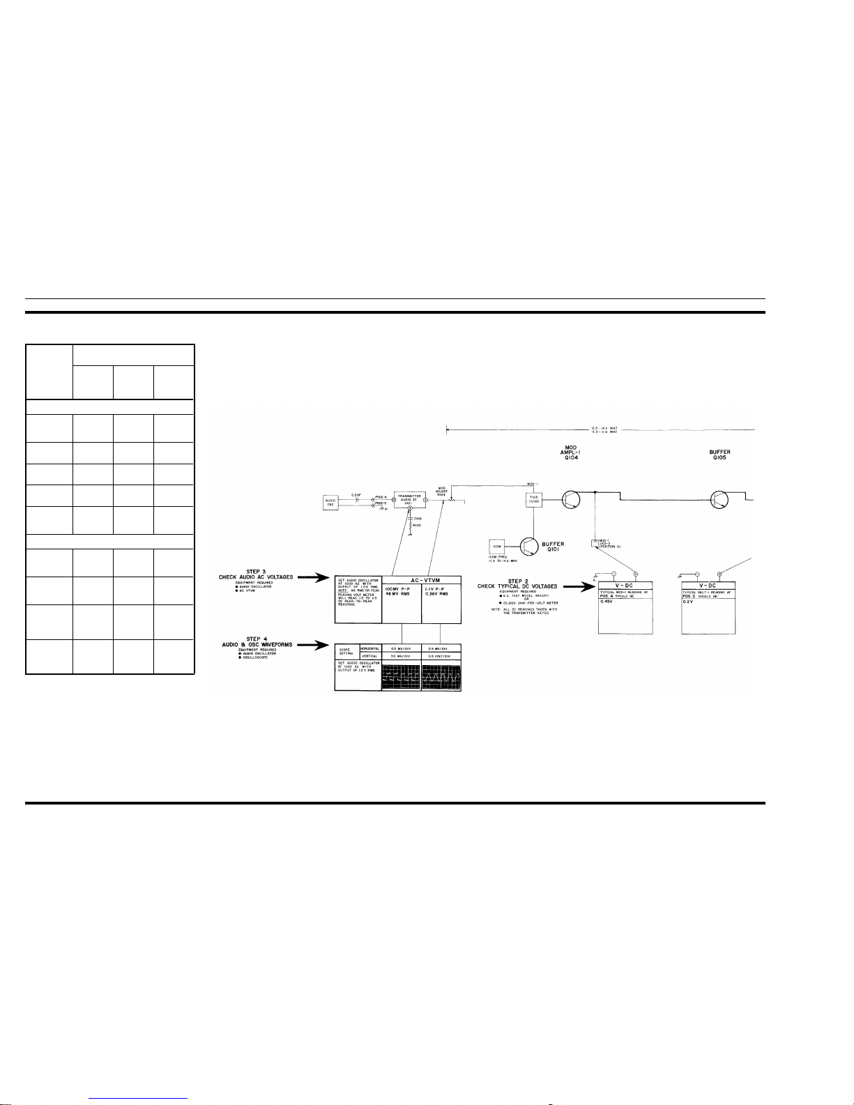
TROUBLESHOOTING PROCEDURE
STEP 1 - QUICK CHECKS
METER
POSITION GE
TEST SET
PROBABLE DEFECTIVE STAGE
HIGH
METER
READING
LOW METER
READING
ZERO
METER
READING
EXCITER
B
(MOD-1)
Q102, 10Volt Regulator
T103,
CV103, C104
T103,
CV103,
CR104, Q104
C
(MULT-1)
Q105, Q106,
T104
Q105, Q106 Q105, Q106,
T104
D
(MULT-2)
Q107, T106 T104, T104,
Q107
T104, T105,
Q107, T106
F
(MULT-3)
Q108, T108 T106, T107,
Q108
T106, T107,
Q108, T108
G
(AMPL-1)
Q109, C157 T108, T109,
T110, Q109
T108, T109,
T110, Q109,
L106
POWER AMPLIFIER
"C"
(TRIPLER
DRIVE)
Low Output
from Exciter
No output
from Exciter
CR201
"D"
(AMPL-2
INPUT)
Q207 Q207 Q207, Q201
"F"
(DRIVER
CURRENT)
Q204 Q204, Low
Output from
Q201, Q207,
Q202, Q203
Q203, Q202,
Q207, Q201.
Check Pos. C
& D
"G"
(PA CURRENT)
Q205, Q206 Q201, Q207,
Q202, Q203,
Q204, Q205,
Q206
Q206, Q205,
Q204, Q203,
Q202, Q207,
Q201, Q215
LBI-4622 LBI-4622
10
Page 12
406-512 MHz, 40-WATT TRANSMITTER
Issue 2
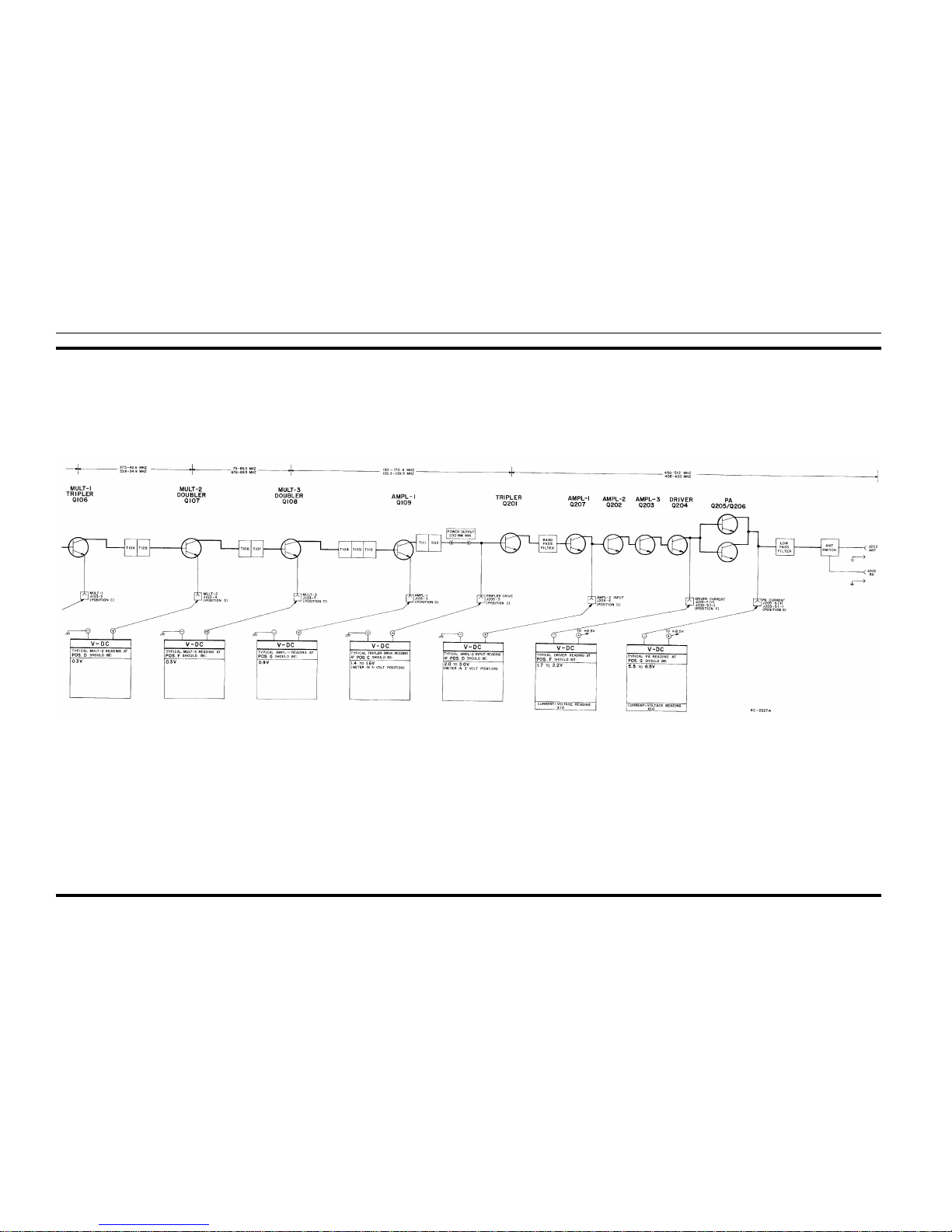
TROUBLESHOOTING PROCEDURE
LBI-4622 LBI-4622
11
Page 13
406-512 MHz, 40-WATT TRANSMITTER
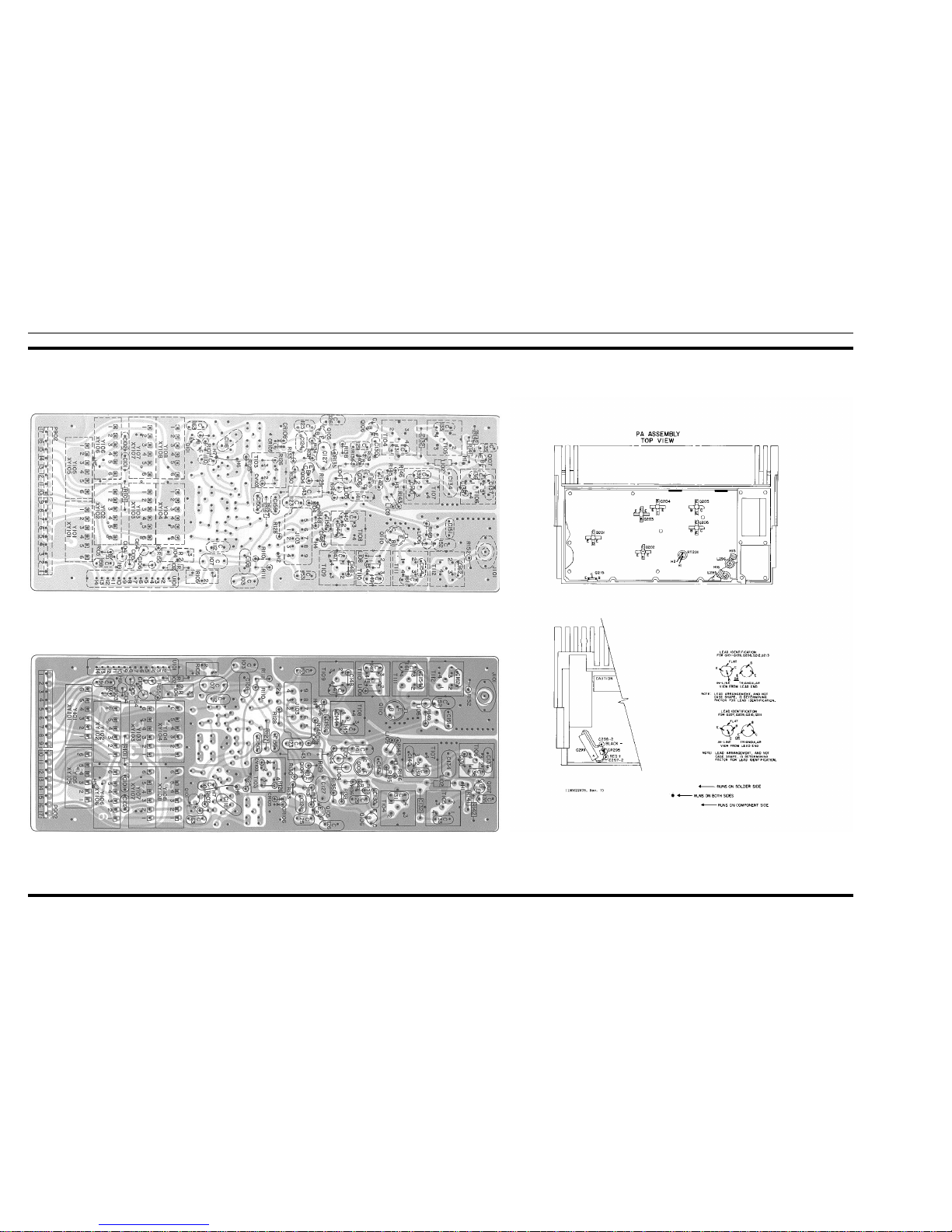
OUTLINE DIAGRAM
EXCITER BOARD
SOLDER SIDE
(19D416850, Sh. 2, Rev. 3)
COMPONENT SIDE
(19D416850, Sh. 2, Rev. 3)
(19D416850, Sh. 3, Rev. 3)
LBI-4622 LBI-4622
12
Page 14
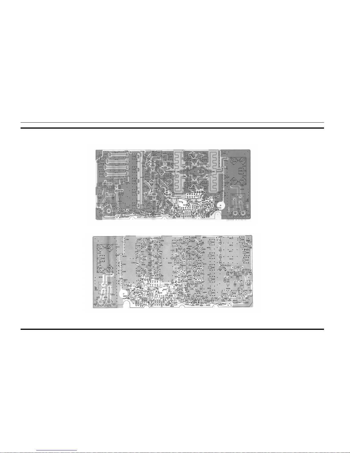
PA BOARD
OUTLINE DIAGRAM
(19D417162, Sh. 2, Rev. 3)
(19D417162, Sh. 3, Rev. 5)
COMPONENT SIDE
(19D417162, Sh. 2, Rev. 3)
SOLDER SIDE
LBI-4622 LBI-4622
13
Page 15
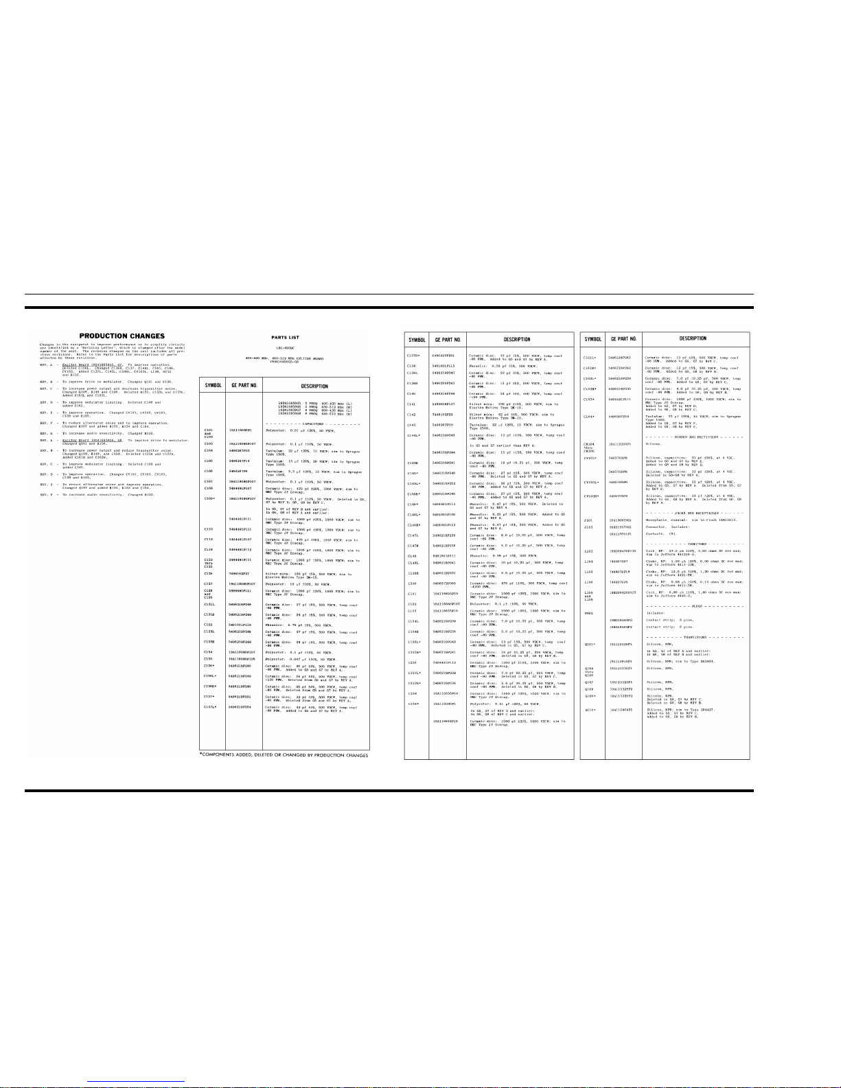
PARTS LIST
LBI-4622 LBI-4622
14
Page 16
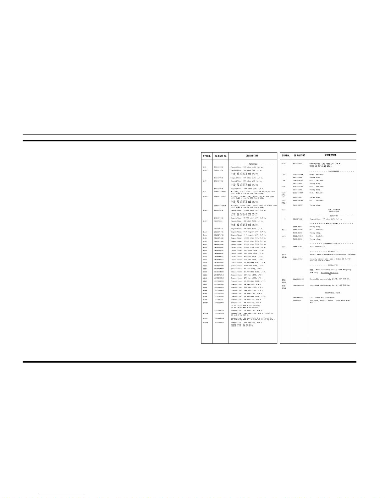
PARTS LIST
LBI-4622 LBI-4622
15
Page 17
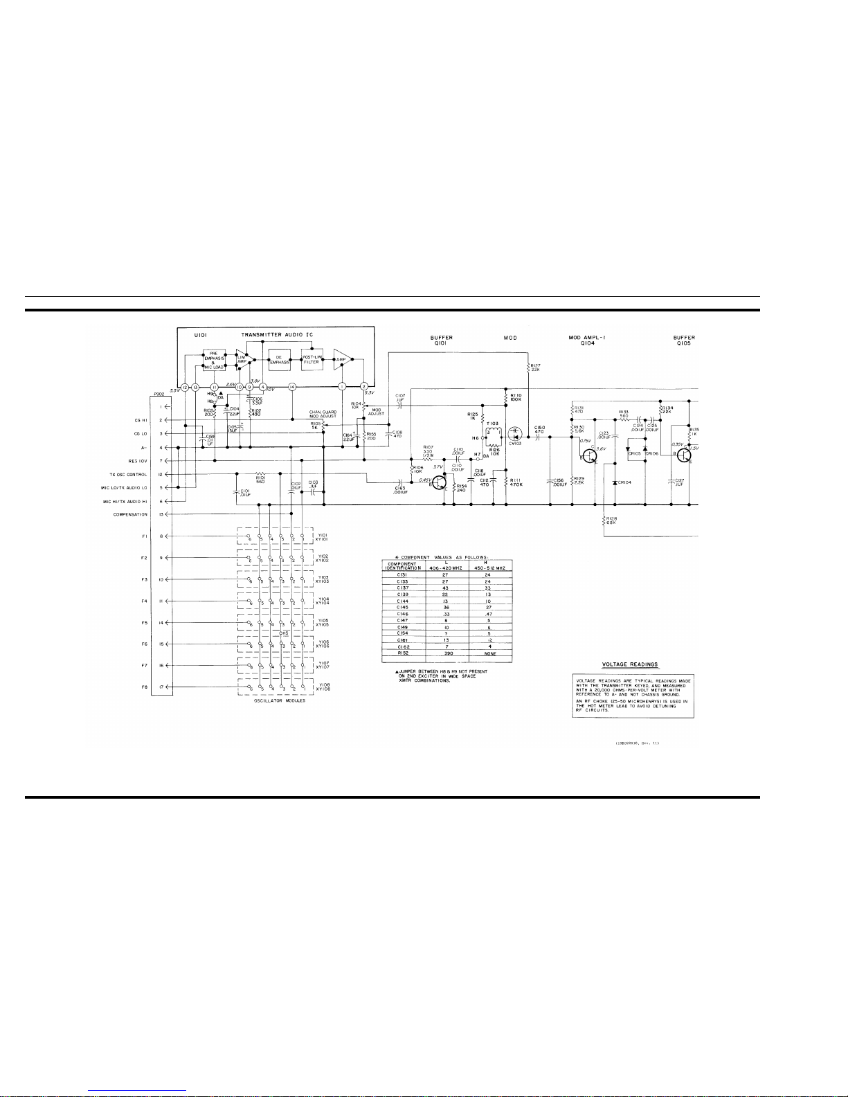
406-512 MHz, EXCITER BOARD
19D416859G5-G8
SCHEMATIC DIAGRAM
LBI-4622 LBI-4622
16
Page 18
406-512 MHz, EXCITER BOARD
19D416859G5-G8
SCHEMATIC DIAGRAM
LBI-4622 LBI-4622
17
Page 19
406-512 MHz, 40-WATT POWER AMPLIFIER
19C320620G5-G8
SCHEMATIC DIAGRAM
LBI-4622 LBI-4622
18
Page 20
406-512 MHz, 40-WATT POWER AMPLIFIER
19C320620G5-G8
SCHEMATIC DIAGRAM
LBI-4622 LBI-4622
19
Page 21
406-512 MHz, 40-WATT POWER AMPLIFIER
19C320620G5-G8
SCHEMATIC DIAGRAM PARTS LIST
LBI-4622 LBI-4622
20
Page 22
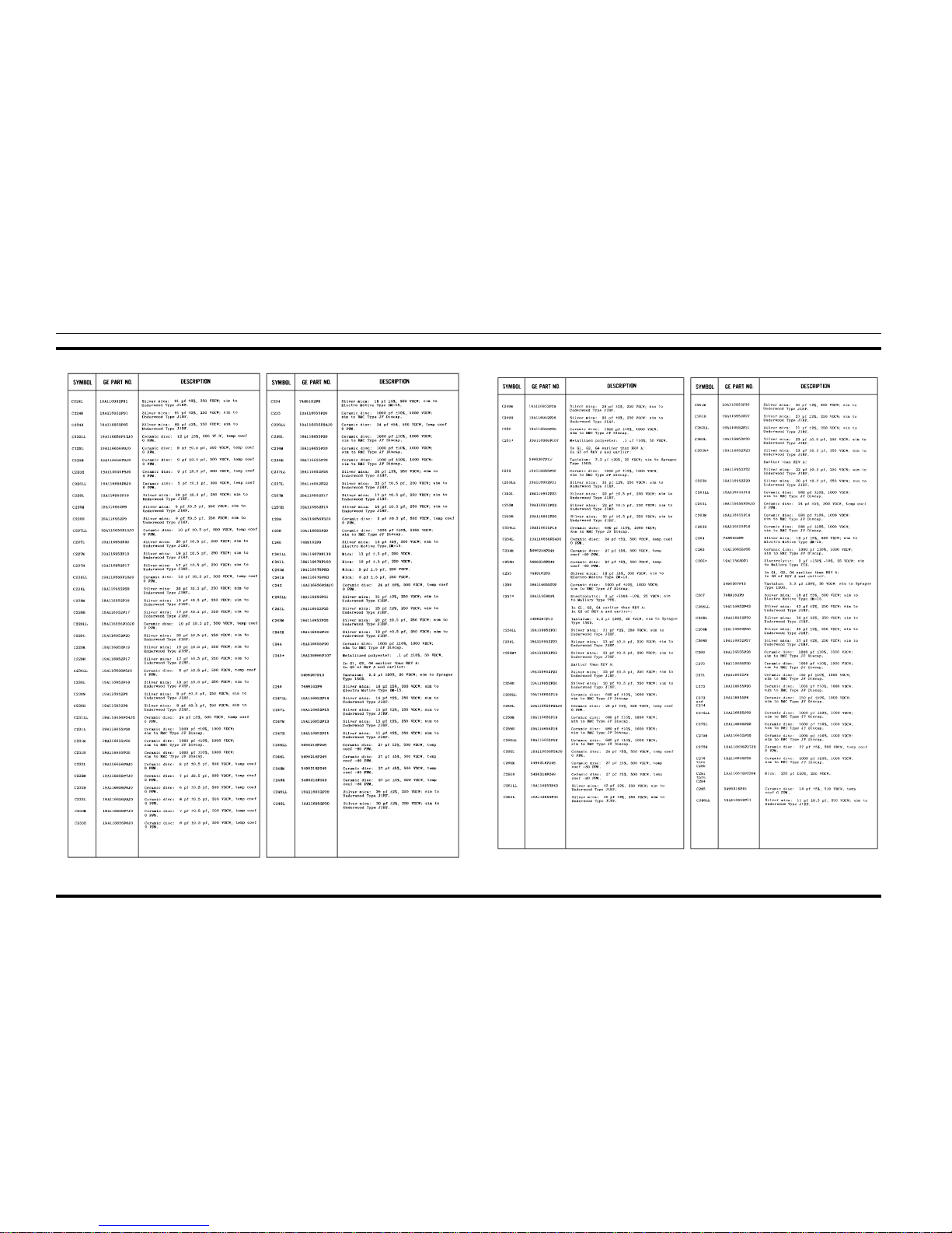
PARTS LIST
LBI-4622 LBI-4622
21
Page 23
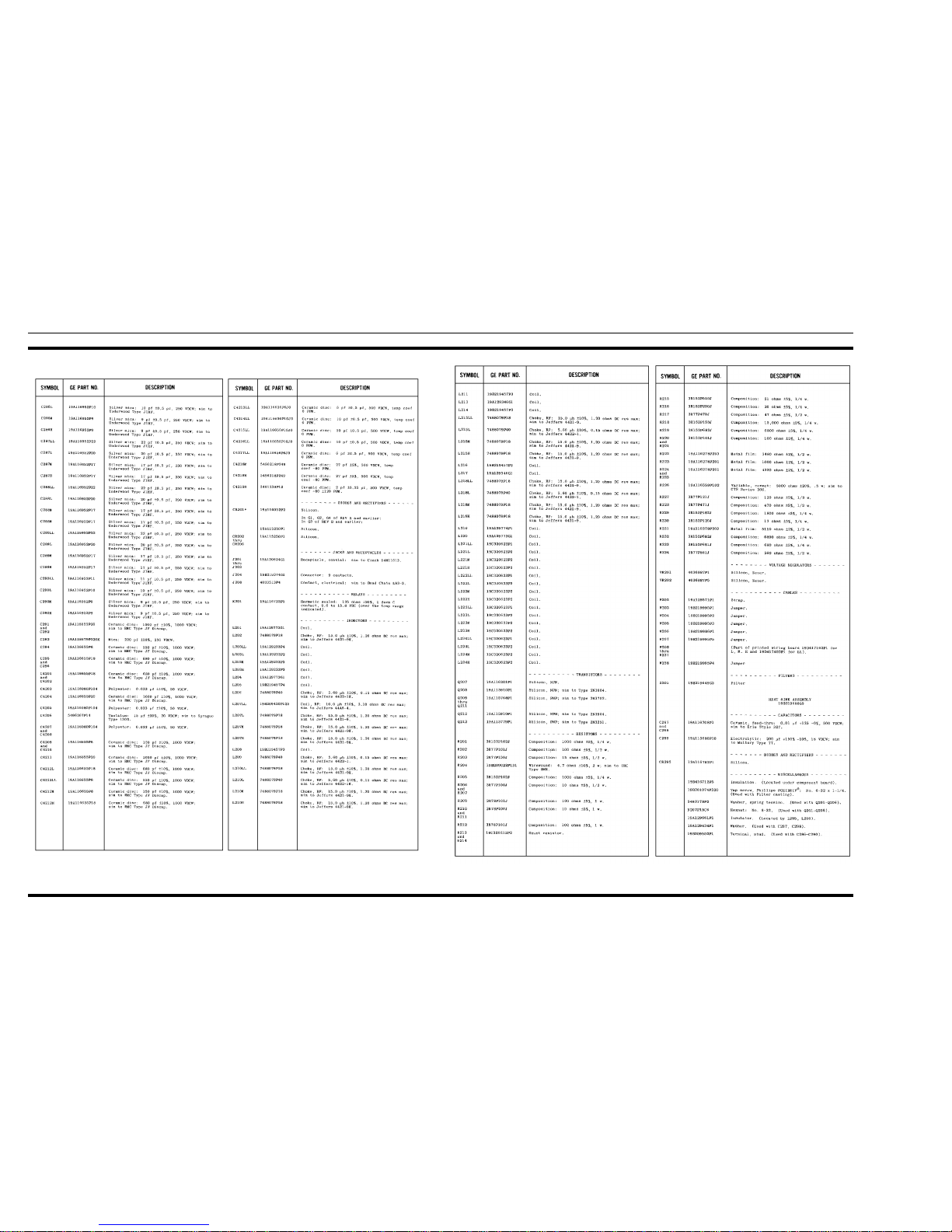
PARTS LIST
LBI-4622 LBI-4622
22
Page 24
LBI-4622 LBI-4622
23
 Loading...