

Page 1

Maintenance Manual
LBI-38128A
Printed in U.S.A.
Mobile Communications
150-174 MHz, 110 WATT POWER
AMPLIFIER 19D901865G1
136-174 MHz, 40 WATT POWER
AMPLIFIER 19D901865G2,3
Page 2
DESCRIPTION
The PA assembly uses five RF power transistors to provide
110 watts of output power, o r 3 RF transistors to p rovide 40 watts
of output power. The output power is adjustable over a ran ge o f
55 to 110 watts in the high power PA, and 20 to 40 watts in the
medium power P A . Five trans istors are u sed in the p ower contr ol
circuit.
Supply voltage for the PA is connected from power leads on
the Transmit-Receive-System (TRS) boar d through feedthrough
capacitors A2-C1 and C2 to h ole 1 1 (A-) and hole 12 (A+) on the
PA board. C52, C53, and L23, and L24 prevent RF from getting
on the power leads. Diode D 5 will cause the m ain fuse in the fuse
assembly to blow if the polarity of the power leads is reversed.
The PA assembly is insulated from vehicle ground by C33
through C44 to permit operation in positive or negative ground
vehicles.
PA metering Jack J1 is provided for use with GE Test Set
Model 4EX3A11 or Test Kit 4EX8K12 with a cable adapto r. The
Test Set meters the RF drive (exciter output), control voltage
driver current, PA current and PA voltage.
CIRCUIT ANALYSIS
RF AMPLIFIERS
The exciter output is coupled through P101 on the TRS
board to PA input jack J3. The RF is coupled through a 50 ohm
stripline (Z5) and then through T1, stripline Z6, L1 and Z7 to the
base of 1st RF Driver Q1.
Part of the RF is rectified by D1 and applied to RF Switch
Q13 to activate the power control circuitry. Part of the DC
voltage is applied t o volta ge divi ders R1 a nd R2 for m eter ing the
exciter output at J1.
The RF amplifiers consist of three Class C , common-emitter
amplifiers. In 40 wa tt transmitters, Q3 is the PA stage. R17, L12
and L42 are a stabilizing network in the base of Q3. The output
of Q3 is coupled through 50 ohm coaxial cable W6 to the low
pass filter and then to the antenna relay.
Driver current is metered at J1 (Driver Current). The reading
is taken on the one-volt scale with the High Sensitivity button
pressed, and with the meter polarity switch in the minus (-)
position. The meter is read as 15 amperes full scale. Jumpers W3,
W5 and W7 act as shunt resistors for the metering circuit.
In 110 watt transmitters, the 40 watt output is coupled
through jumper W1 to a Wilkinson power splitter consisting of
C57, C59, L26, L27 and Z1.
The power amplifier stages consist of two identical paralleled Class C power amplifiers (Q5 and Q6).
L30, L32, R24 a nd C63 make up a s t abilizing network in
the base of Q5, while L31, L33, R25 and C68 make up the
stabilizing network in the base of Q6. Supply voltage (A+) for
Q5 and Q6 is coupled through collector feed networks Z 3 and
Z4.
Collector current for Q5 and Q6 is measured at J1 (PA
Current). The reading is taken on the one-volt scale with the
high sensitivity button pressed and the polarity switch in the
minus (-) position. The current is read as 30 amperes full scale.
The output of Q5 and Q6 is applied to a Wilkinson power
combiner consisting of C78, L40, Z2, L41 and C79. The output
of the combiner is coupled through T2 and two 50 ohm
striplines (Z16 and Z17) to the low pass filte r. The filter output
is coupled through 50 ohm stripline to Z18 to the antenna relay
(K1).
POWER CONTROL CIRCUIT
The power control circuit provides power leveling as well
as thermal protection for the PA.
When the transmitter is keyed, RF is rectified by D1. The
resulting DC turns on RF switch Q13. This allows Q11, Q12
and pass transistor Q4 to turn on. Turning on Q4 applies
collector voltage to 1st RF d ri v er Q 1.
If the power output should start to increase above th e level
set by R23, Q14 will start to conduct. This causes Q12, Q11
and Q13 to conduct less, reducing the collector voltage to the
1st RF driver.
Thermal protection is provided by temperature compensating resistor R19. As the heat sink temperature rises above
70
o
C, the resistance of R19 decreases. This causes Q3, Q11,
and Q12 to conduct less, reducing the power output.
Copyright© June 1988, General Electric Company
TABLE OF CONTENTS
PAGE
DESCRIPTION...................................................................................................................................... 1
CIRCUIT ANALYSIS........................................................................................................................... 1
SCHEMATIC DIAGRAM .................................................................................................................... 3
OUTLINE DIAGRAM .......................................................................................................................... 4
PARTS LIST.......................................................................................................................................... 6
NOTE
In positive ground vehicles, A- is "hot" with respect to
vehicle ground. Shorting the transmitter PA printed
wiring board ground p attern to th e radio cas e may cause
one of the in-line fuses to blow.
Do not operate the transmitter at levels higher than
rated output. Operating at higher than rated output
will shorten the life of the RF power transistor.
CAUTION
The RF Power Transistors used in the transmitter
contain Beryilium Oxide, A TOXIC substance. If the
ceramic, or other encapsulation is opened, crushed,
broken or abraded, the dust may be hazardous if
inhaled. Use care in replacing transistors of this type.
WARNING
LBI-38128 LBI-38128
1
Page 3
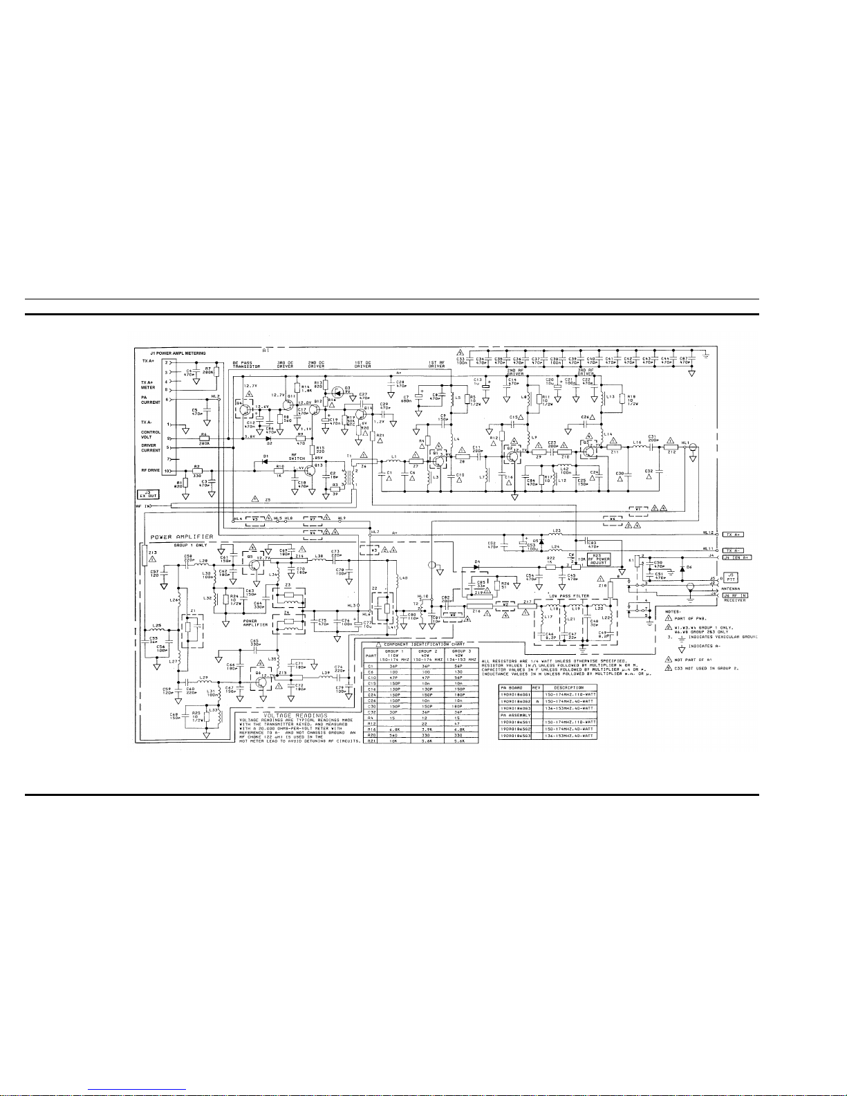
Schematic Diagram
POWER AMPLIFIER
19D901861
LBI-38128 LBI-38128
2
Page 4
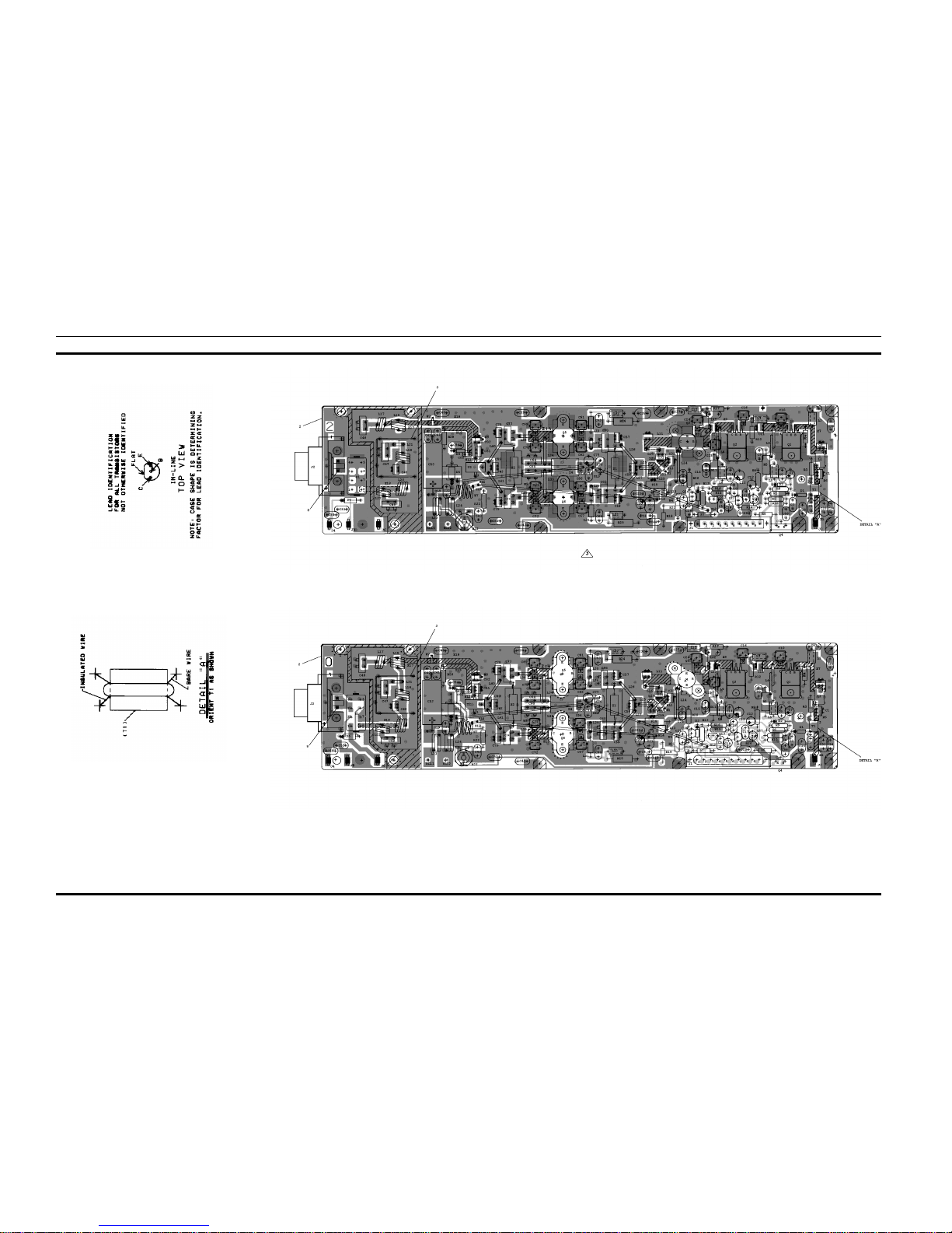
Printed Wiring Diagram
POWER AMPLIFIER BOARD
19D901860G1-G3
LBI-38128 LBI-38128
3
Page 5
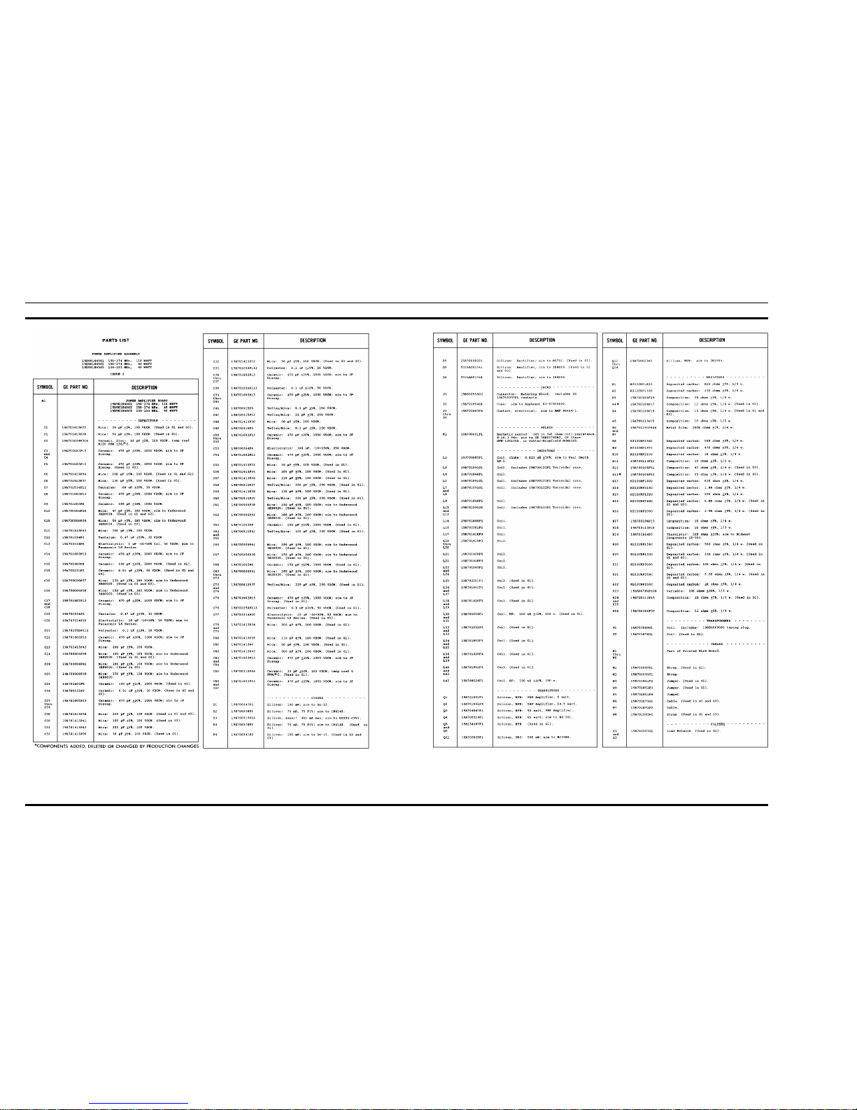
Parts List
LBI-38128 LBI-38128
4
Page 6
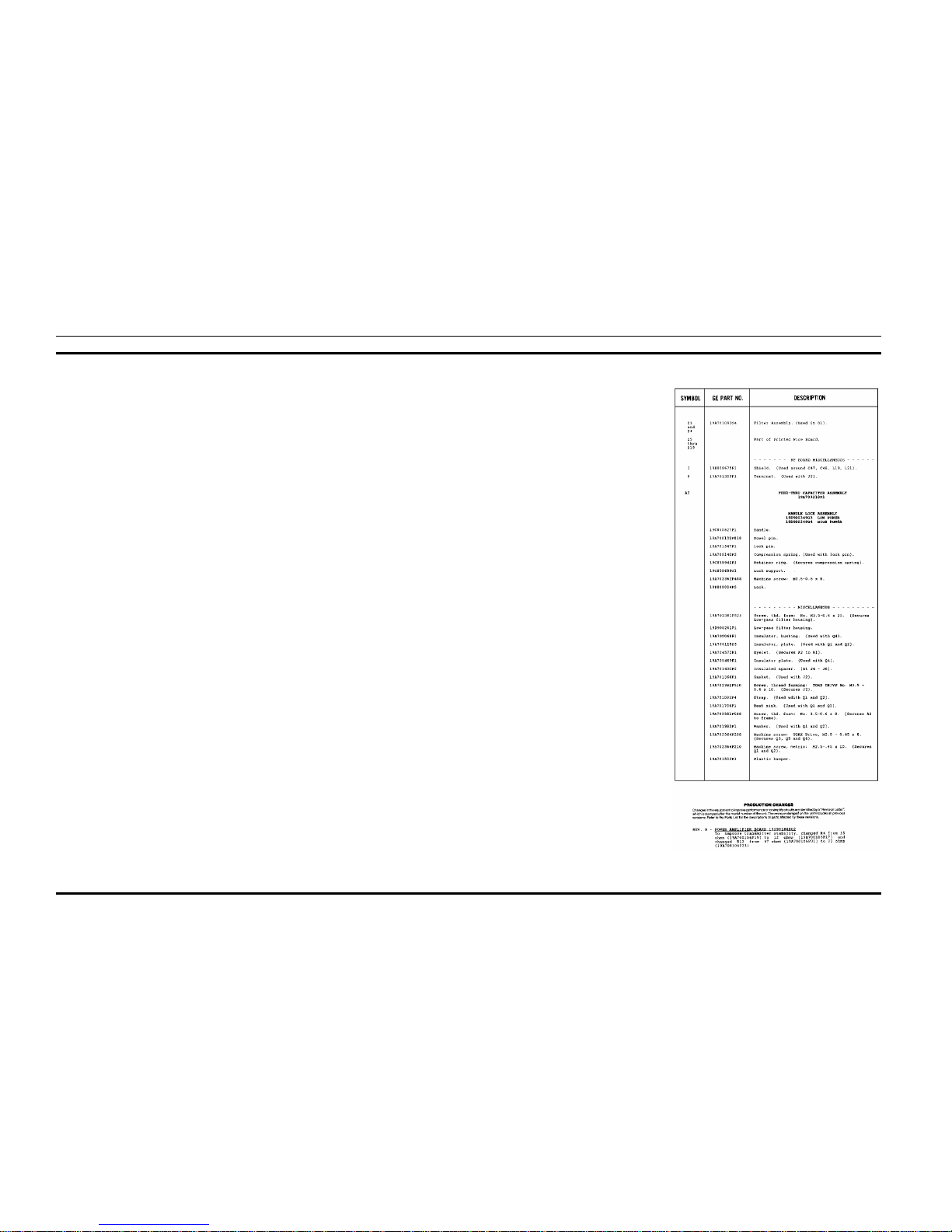
Parts List
LBI-38128 LBI-38128
5
 Loading...