

Page 1
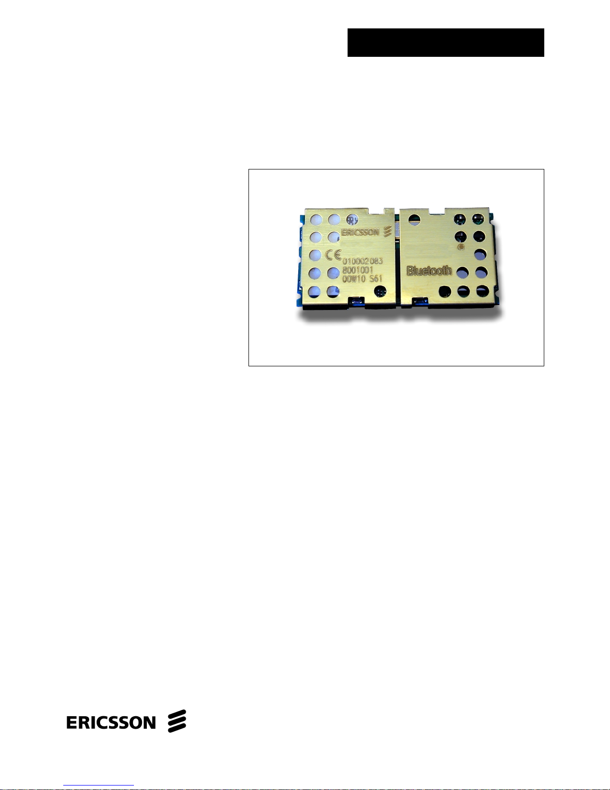
ROK 101 007
Bluetooth Module
Description
ROK 101 007 is a short-range module for implementing Bluetooth functionality into various electronic devices. The module consists of three major
parts; a baseband controller, a flash memory, and a radio that operates in the
globally available 2.4–2.5 GHz free ISM band.
Both data and voice transmission is supported by the module. Communication between the module and the host controller is carried out using a highspeed USB interface compliant with USB Specifications 1.1 or an UART/
PCM interface. When using the USB interface, the module appears as a USB
slave device and therefore requires no PC resources.
ROK 101 007, which is compliant with Bluetooth version 1.0B, is a Class 2
Bluetooth Module (0 dBm) and is type-approved. The module supports all
Bluetooth profiles.
Key Features
• Pre-qualified Bluetooth 1.0B Module
• RF output power class 2
• FCC and ETSI approved
• 460 kb/s max data rate over UART
• Multiple interface for different
applications
-UART for data
-PCM for voice
-USB for voice and data
•I
2
C interface
• Internal crystal oscillator
• HCI firmware included
• Multi Point Operation
• Built-in shielding
Suggested Applications
• Computers and peripherals
• Handheld devices and accessories
• Access points
ROK 101 007
Page 2
ROK 101 007
2
Preliminary
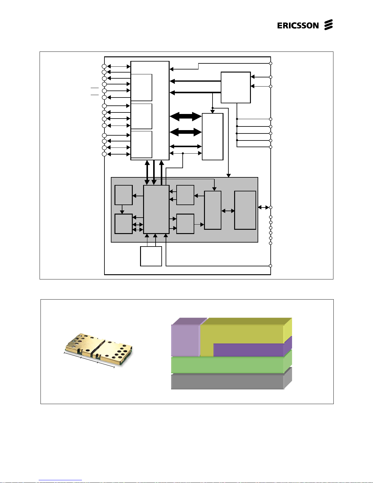
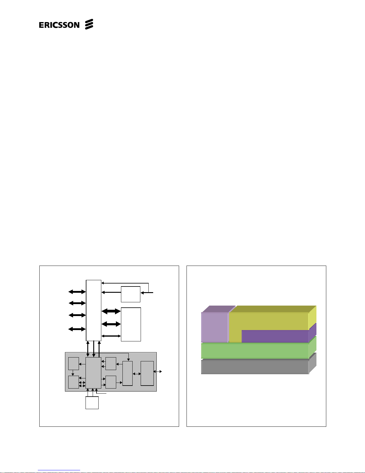
Figure 1. Block Diagram
Figure 2. Actual size of the Ericsson Bluetooth Module, and also showing the HW and FW stack.
RX-
Balun
Radio
ASIC
ANT
T2
TX-
Balun
Switch
Antenna
Filter
Loop
Filter
VCO
Tank
FLASH
Memory
13MHz
Crystal
Voltage
Regulation
WAKE_UP
DETACH
GND
B3
R1
R2
T1
C6
VCC
C4
VCC_IO
C2
ON
RESET#
POR
NC
NC
NC
NC
NC
R4
R5
R6
T4
T5
T6
C3
Radio Module
B4
C1
ADDR
DATA
CTRL
R3
C5
NC
PBA 313 01/2
Baseband
B1
D-
D+
B2
USB
TXD
RTS
RXD
CTS
A5
A6
B5
B6
UART
PCM_OUT
PCM_CLK
PCM_IN
PCM_SYNC
A1
A2
A3
A4
PCM
T3
GND
GND
GND
GND
I2C_DATA
I2C_CLK
0123 cm
Radio
Baseband
Audio
Link Manager
HCI
Page 3
ROK 101 007
3
Preliminary
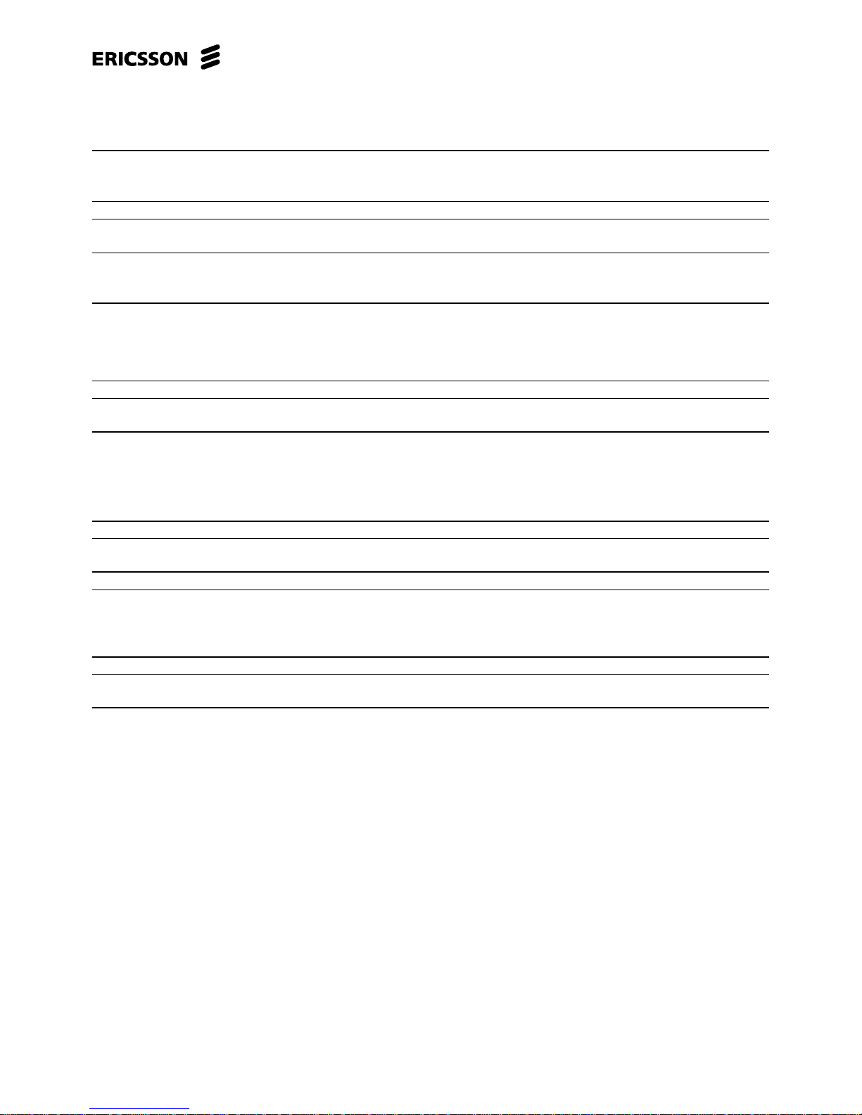
Absolute Maximum Ratings
Parameter Symbol Min Typ Max Unit
Temperature
Storage temperature T
Stg
-30 +85 °C
Operating temperature T
Amb
0 +75 °C
Power Supply
V
CC
V
CC
-0.3 +5.25 V
V
CC_IO
V
CC_IO
-0.8 +3.6 V
Digital Inputs
Input low voltage V
IL
-0.5 V
Input high voltage V
IH
V
CC_IO
+0.3 V
Recommended Operating Conditions
Temperature
Ambient temperature, Test T
amb
+23 °C
Power Supply
Positive Supply Voltage V
CC
+3.3 V
I/O Ports Supply Voltage V
CC_IO
+3.3 V
Electrical Characteristics
DC Specifications
Unless otherwise noted, the specification applies for T
Amb
= 0 to +75°C, 3.175 < VCC < 5.25V
Parameter Condition Symbol Min Typ Max Unit
Power Supply
Supply Voltage V
CC
3.175 3.3 5.25 V
I/O Ports Supply Voltage See note 10 V
CC_IO
2.7 3.3 3.6 V
Digital Inputs
Logical Input High Except ON signal V
IH1
0.7 x V
CC_IO
V
CC_IO
V
Logical Input Low Except ON signal V
IL2
0 0.3 x V
CC_IO
V
Logical Input High ON signal only V
IH2
2.0 V
CC
V
Logical Input Low ON signal only V
IL2
0 0.4 V
Digital Outputs
Logical Output High V
OH
0.9 x V
CC_IO
V
CC_IO
V
Logical Output Low V
OL
0 0.1 x V
CC_IO
V
Page 4
ROK 101 007
4
Preliminary
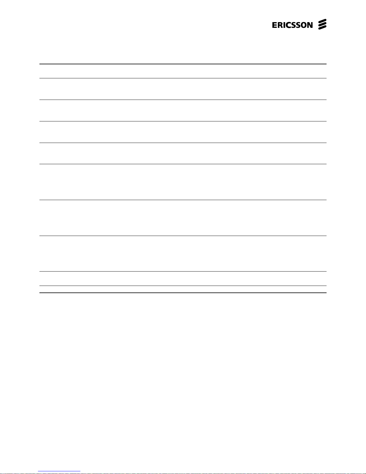
5Parameter Condition Symbol Min Typ Max Unit
Average Current
Consumption Average ICC + I
CC_IO
Standby I
STA
5.95 mA
Shutdown - SW I
SSW
2.35 mA
Shutdown – HW See note 1 I
SHW
1 µA
Page Scan Mode R0 Page Scan Enable I
PSM1
50 mA
Page scan window: continuous
Page scan interval : n/a (0s)
Page Scan Mode R1 Page Scan Enable I
PSM2
6.35 mA
Page scan window: 11.25ms
Page scan interval : 1.28s
Page Scan Mode R2 Page Scan Enable I
PSM3
6.15 mA
Page scan window: 11.25ms
Page scan interval : 2.56s
Inquiry Scan Inquiry Scan Enable I
ISM1
50 mA
with Page Scan Mode R0. Page Scan Window : 2.56s –11.25ms
Page Scan Interval : 2.56s
Inquiry Scan Window : 11.25ms
Inquiry Scan Interval : 2.56s
Inquiry Scan Inquiry Scan Enable I
ISM2
6.55 mA
with Page Scan Mode R1. Page Scan Window : 11.25ms
Page Scan Interval : 1.28s
Inquiry Scan Window : 11.25ms
Inquiry Scan Interval : 2.56s
Inquiry Scan Inquiry Scan Enable I
ISM3
6.35 mA
with Page Scan Mode R2. Page Scan Window : 11.25ms
Page Scan Interval : 2.56s
Inquiry Scan Window : 11.25ms
Inquiry Scan Interval : 2.56s
Connect State Established connection I
CS
26 mA
with data transfer
V
CC_IO
Current Only I
CC_IO
, V
CC_IO=TBD
I
CC_IO
TBD mA
Page 5
ROK 101 007
5
Preliminary
RF Specifications
Parameter Condition Symbol Min Typ Max Unit
General
Frequency Range 2.402 2.480 GHz
Double Sided IF Bandwidth 1 MHz
Antenna load 50 Ω
VSWR RX mode 3:1
VSWR TX mode, see note 2 3:1
Receive Performance
Sensitivity level P
IN
: -70dBm, 0.1% BER
75kHz offset (max),
Max input level P
IN
: -20dBm, 0.1% BER
75kHz offset (max),
C/I
co-channel
C: -60 dBm 14 dB
C/I
1MHz
C: -60 dBm +4 dB
C/I
2MHz
C: -60 dBm -30 dB
C/I
≥3MHz
C: -67 dBm -40 dB
Blocking, C/I
DC-5GHz
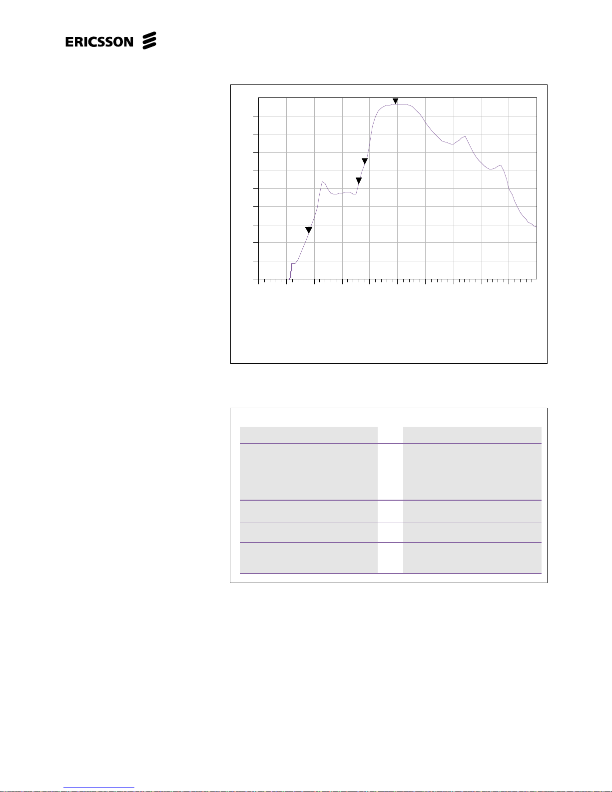
See figure 6
Out-of-band blocking 30-1910 MHz +4 dBm
1910-2000 MHz -10 dBm
2000-2399 MHz -27 dBm
2484-3000 MHz -27 dBm
3.00-12.75 GHz -10 dBm
Spurious Emissions 30 MHz to 1 GHz -57 dBm
Spurious Emissions 1 GHz to 12.75 GHz -47 dBm
Transmitter Performance
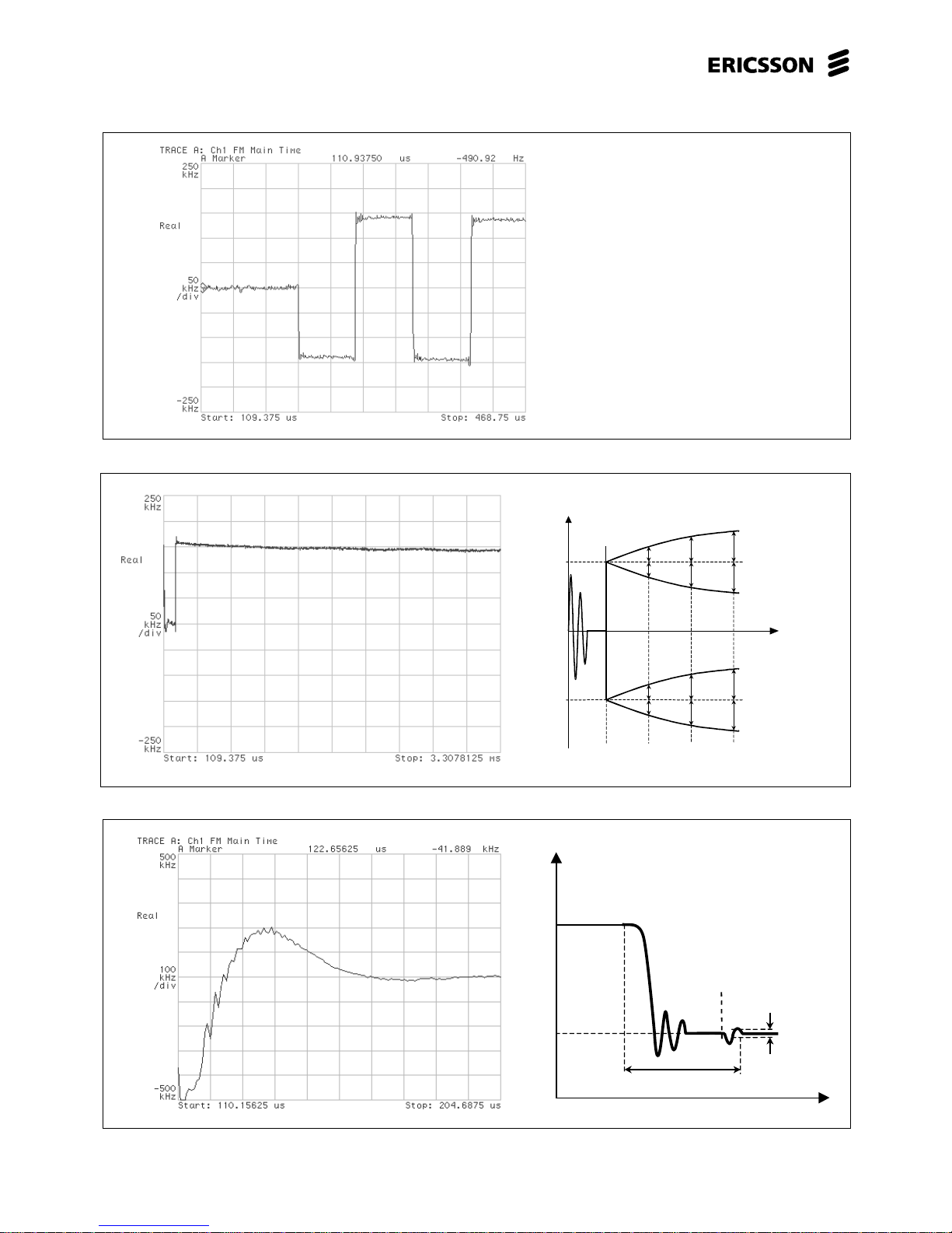
Frequency deviation see notes 3,4 f
Mod
140 175 kHz
and figure 3
Initial frequency error see note 5 -48 +48 kHz
TX power -2 1.5 4 dBm
TX carrier drift in 1 slot (366 µs) f
Drift1
-25 25 kHz
TX carrier drift in 3 slots (1598 µs) f
Drift2
-40 40 kHz
TX carrier drift in 5 slots (2862 µs) see figure 4 f
Drift3
-40 40 kHz
20 dB bandwidth Measured with RBW: 10 kHz and peak detector 1.000 MHz
Spurious Emissions 30 MHz – 1GHz -36 dBm
Spurious Emissions 1 GHz – 12.75 GHz -30 dBm
Spurious Emissions 1.8 Hz – 1.9 GHz -47 dBm
Spurious Emissions 5.15 GHz – 5.3 GHz -47 dBm
Timing performance
LPO_CLK frequency Trimmed, see note 6 f
LPO_CLK
3,2 kHz
Tolerance of LPO_CLK see note 6 -250 +250 ppm
System clock frequency f
SYS_CLK
13.0000 MHz
Tolerance of system clock see note 5 -20 +20 ppm
Channel switching time see figure 5 150 µs
Received Signal Strength Indicator
RSSI Input power = -40 dBm 15 25 n/a
RSSI Input power = -60 dBm 3 11 n/a
Page 6
ROK 101 007
6
Preliminary
t
D
f
TX carrier
drift
PHD_OFF
t=214 µs
+f
dev
-f
dev
t=580 µs
t=1598 µs t=2862 µs
SYNT_ON
TX_ON
TX_DATA: High
TX_DATA: Low
New
ch.
Old
ch.
50 kHz
Channel switching time
t
f
SYNT_ON
TX_ON
Figure 5. Channel switching time
Figure 3. Frequency Deviation
PHD_OFF
TX_DATA: High
TX_DATA: 64 logic 'Low' & 64 logic 'High'
See note 4
Figure 4. Frequency drift.
RF Specifications continued...
Page 7
ROK 101 007
7
Preliminary
C/I Blocking
The blocking characteristics can be
basically split into two regions: Inband and Out-of-band. Blocking is
performed both on the chip and on
the module level.
• In-band
– Filtering on chip
– C/I @ 2MHz: -30 dB -> 0.1%BER
– C/I ≥ 3MHz: -40 dB -> 0.1%BER
• Out-of-band
– Antenna filter, DC to 1.9 GHz and
3:rd harmonic.
– Switch, low freq. and 2:nd har-
monic.
– RX-balun, low freq. and 2:nd
harmonic.
– On-chip IF filter
Figure 6 shows the combination
blocking effect of the antenna switch,
antenna filter and RX balun. In
addition to the blocking characteristics shown in figure 6, there is
antenna isolation and filtering on the
chip.
Marker 1 shows the region where the
Bluetooth band is located. Markers 2
- 4 show the blocking at the telecom
frequency bands.
An example of the total blocking
characteristics can be seen in figure 7.
0.0 0.5 1.0 1.5 2.0 2.5 3.0 3.5 4.0 4.5 5.0
GHz
-100
-90
-80
-70
-60
-50
-40
-30
-20
-10
0
m1
freq=2.450GHz
dB( RX path)=- 3.529
m
1
m2
freq=900.0MHz
dB(RX path) =-74.580
m
2
m3
freq=1.800GHz
=-47.426
m
3
m4
freq=1.900GHz
)=-36.537
m4
dB(RX path)
dB(RX path)
dB(RX path
Figure 6. Typical blocking characteristics excluding antenna
isolation and on chip filtering.
Example 2
Interference of +33 dBm at 1910 MHz.
Antenna isolation 25 dB
Antenna filter, 36 dB
Antenna switch,
RX-balun
Interference level before
IF filter
+33-25-36=
-28 dBm
0.1% BER carrier
level
-40 + (-28)=
-68 dBm
Example 1
Interference of +33 dBm at 2015 MHz.
Antenna isolation 15 dB
Antenna filter, 27 dB
Antenna switch,
RX-balun
Interference level before
IF filter
+33-15-27=
-9 dBm
0.1% BER carrier
level
-40 + (-9)=
-49 dBm
0.1% BER requires a C/I of more than -40 dB at the IF filter.
Figure 7. Blocking examples.
RF Specifications continued...
Page 8
ROK 101 007
8
Preliminary
Pin Description
Pin Pin Name Type Direction Description
A1 PCM_IN CMOS In PCM data, see notes 7,9
A2 PCM_OUT CMOS Out PCM data, see notes 7,9
A3 PCM_SYNC CMOS In/Out Sets the PCM data sampling rate, see notes 7,9
A4 PCM_CLK CMOS In/Out PCM clock that sets the PCM data rate, see notes 7,9
A5 RXD CMOS Input RX data to the UART, see note 9
A6 RTS CMOS Input Flow control signal, Request To Send data from UART, see notes 7,9
B1 D+ CMOS In/Out USB data pin, see notes 9,10
B2 D- CMOS In/Out USB data pin, see notes 9,10
B3 GND Power Power Signal ground
B4 WAKE_UP CMOS Output Indicates that the module wants to be attached to the USB,
Active High. See notes 9,10
B5 TXD CMOS Output TX data from the UART, see note 9
B6 CTS CMOS Output Flow control signal, Clear To Send data from UART, see note 9
C1 DETACH CMOS Input Indicates that the USB host wants to detach the module,
Active High. See notes 7,9
C2 ON Power Input When tied to VCC, the module is enabled.
C3 I2C_CLK CMOS Output I2C clock signal, see note 9
C4 VCC_IO Power Power External supply rail to the Input / Output ports
C5 NC - - Do not connect
C6 VCC Power Power Supply Voltage
R1 GND Power Power Signal ground
R2 GND Power Power Signal ground
R3 RESET# CMOS Input Active low reset, see notes 8,9
R4 NC - - Do not connect
R5 NC - - Do not connect
R6 NC - - Do not connect
T1 GND Power Power Signal Ground
T2 ANT RF In/Out 50Ω Antenna connection
T3 GND Power Power Signal Ground
T4 NC Power Power Test point, internal voltage regulator - Do not connect
T5 NC - - Do not connect
T6 I2C_DATA CMOS In/Out I2C data signal, see note 9
Notes
1. Current consumption is based upon when the module is when ‘ON’ is low and ‘VCC_IO’ is grounded.
2. During the TX mode, the VSWR specification states the limits that are acceptable before any other RF parameters
are strongly effected, i.e. frequency deviation and initial frequency error.
3. Frequency deviation measurements are now recorded differentially, (f Mod1 - f Mod0 ) / 2.
4. Provided that the TX INV register (bit 0) has been set in the enable register at startup.
5. Tolerance for the system clock takes into account both the complete temperature range and aging of the crystal.
6. LPO_CLK frequency is pre-trimmed within a tolerance of ±250ppm.
7. 100kΩ pull-up resistors to V
CC_IO
are used on the module. PCM signals direction is programmable
8. RESET# signal must be fed from an open drain output.
9. CMOS buffers are low voltage TTL compatible signals.
10. To be compliant with the USB specification, VCC_IO ≥ 3.11V
Page 9
ROK 101 007
9
Preliminary
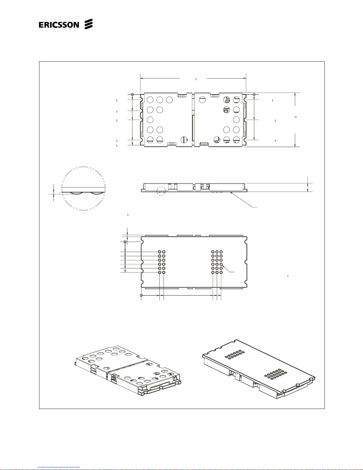
Figure 8. Mechanical dimensions.
Mechanical Specification
2.75 max
without solder balls
Pad size: 35 mil = 0.889 mm
Tolerance on placement: 0.02 mm
approx 0.2 mm
Detail A
Detail A
16.8 0.2
0.54 0.2
Co-planarity 0.1 mm
9.47
32.8 0.2
14.1 0.2
7.85 0.2
1.6 0.2
15.7 0.2
14.1 0.2
7.85 0.2
5.05 0.2
T
R
CBA
6
1
2
3
4
5
5.72
6.98
22.22
23.5
24.76
1.6 0.2
3.12
4.39
5.66
6.93
8.2
Page 10
ROK 101 007
10
Preliminary
USB
Control
VCC
Host
GND
Bluetooth
Module
Wake_up
Detach
GND
VCC_IO ON VCC
D+
D-
4
4
RS 232
transceiver
Codec
PCM
UART
VCC_IO
VCC
RS232
GND
Bluetooth
Module
GND
VCC_IO ON VCC
ON
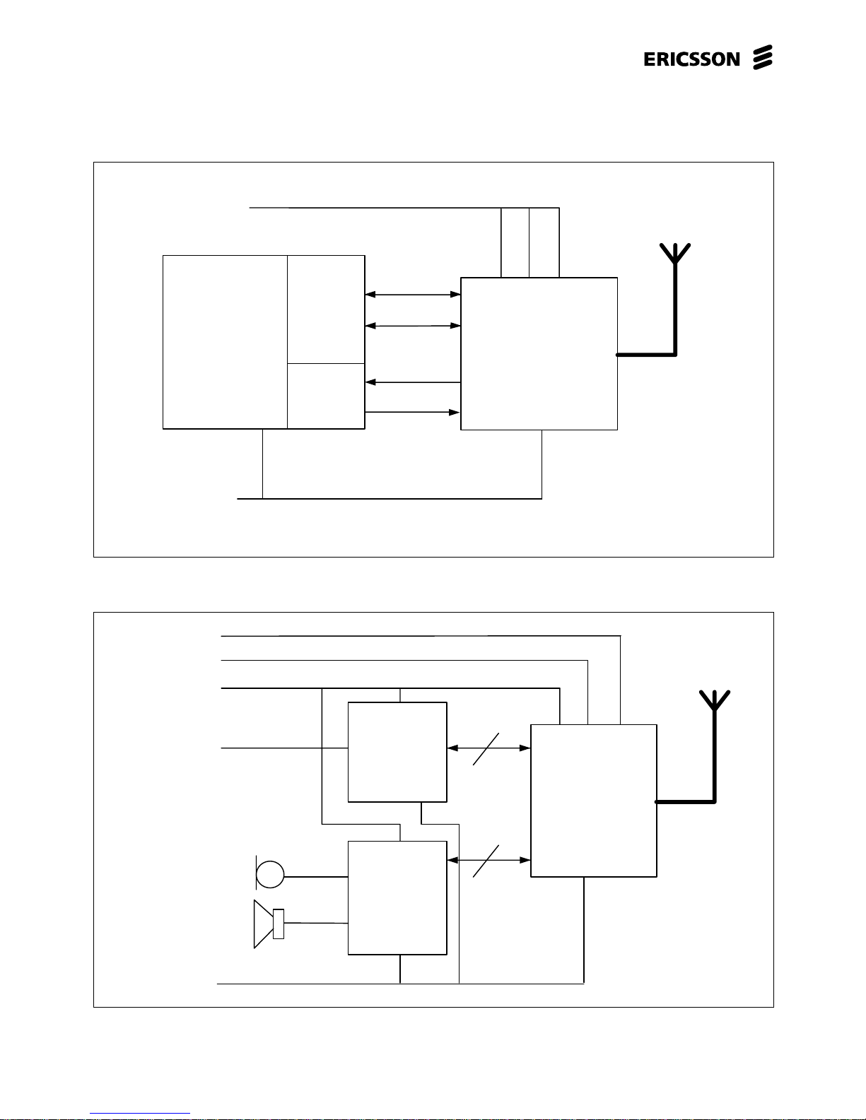
Application Block Schematics
USB Application
Figure 9. A typical USB configuration.
Figure 10. A typical UART or PCM configuration.
UART and PCM Application
Page 11
ROK 101 007
11
Preliminary
Functional Description
The ROK 101 007 is a complete
Bluetooth module that has been
specified and designed according to
the Bluetooth System v1.0B. Its
implementation is based on a highperformance integrated radio transceiver (PBA 313 01 /2) working with a
baseband controller, a flash memory
and surrounding secondary components features low energy consumption for use in battery operated
devices.
Block Diagram
ROK 101 007 has five major operational blocks. Figure 11 illustrates the
interaction of the various blocks. The
functionality of each block is as
follows:
1. Radio functionality is achieved by
using the Bluetooth Radio, PBA
313 01/ 2. Six operational
blocks are shown for the radio
section and their operation is as
follows:
1a) VCO-tank is a part of the phase
locked loop. The modulation is
performed directly on the VCO.
To ensure high performance the
VCO-tank is laser trimmed.
Figure 11. Simplified Block Diagram
RX-
Balun
Radio
ASIC
ANT
TX-
Balun
Switch Antenna
Filter
Loop
Filter
VCO
Tank
Baseband
FLASH
Memory
13MHz
Crystal
Voltage
Regulation
I2C Interface (2)
UART Interface (4)
PCM Voice
Interface (4)
POWER (3)
RESET
ADDR
DATA
CTRL
Radio Module
PBA 313 01/2
1
2
3
4
5
USB Interface (4)
1b) Loop filter, filters the tuning
voltage of the VCO-tank.
1c) RX-balun handles transformation
from unbalanced to balanced
transmission.
1d) TX-balun handles biasing of the
output amplifier stage and
transformation from balanced to
unbalanced transmission.
1e) Antenna switch directs the
power either from the antenna
filter to the receive ports or from
the ASIC output ports to the
antenna filter.
1f) Antenna filter band-pass filters
the radio signal.
2. The baseband controller is an
ARM7-Thumb based chip that
controls the operation of the
radio transceiver via one of the
interface methods; USB or
UART. Additionally, the baseband controller has a PCM Voice
interface and I
2
C interface.
3. A Flash memory is used together
with the baseband controller.
Please, refer also to the
Firmware section.
4. The power management block
regulates and filters the supply
voltage. V
CC
is typically 3.3V and
two regulated voltages are
produced, 2.8V and 2.2V
NOM
.
5. An internal clock is mounted on
the module. The clock frequency
is 13MHz and is generated from
a crystal oscillator that guarantees a timing accuracy within
± 20ppm.
Bluetooth Module stack
The Host Controller Interface (HCI)
handles the communication by the
transport layer through the UART or
USB interface with the host. The
Baseband and radio provides a
secure and reliable radio link for
higher layers.
The following sections describe the
Bluetooth module stack in more
detail. It is implemented in accordance with and complies with the
Specification of the Bluetooth
System v1.0B.
Radio
Baseband
Audio
Link Manager
HCI
Figure 12. HW/FW parts included in the Ericsson
Buetooth module.
Page 12
ROK 101 007
12
Preliminary
Bluetooth Radio Interface
The Bluetooth module is a class 2
device with 4dBm maximum output
power with no power control needed.
Nominal range of the module with a
typical antenna is up to a range of 10
m (at 0 dBm). It is compliant with
FCC and ETSI regulations in the ISM
band.
Baseband
Bluetooth uses an ad-hoc net
structure with a maximum of eight
active units in a single piconet. By
default the first unit setting up a
connection is the master of the point
to point link. The master transmits in
the even timeslots and the slave
transmits in the odd timeslots.
For full duplex transmission, a TimeDivision Duplex (TDD) scheme is
used. Packets are sent over the air in
timeslots, with a nominal length of
625 µs. A packet can be extended to
a maximum of 5 timeslots (DM5 and
DH5 packets) and is then sent by
using the same RF channel for the
entire packet.
Two types of connections are
provided - Asynchronous
Connectionless Link (ACL) for data
and the Synchronous Connection
Oriented Link (SCO) for voice. Three
64 kb/s voice channels can be
supported simultaneously. Furthermore, there are also packages used
for link control purposes.
A variety of different packet types
with error correction schemes and
data rates can be used over the air
interface. Also asymmetric communication is available for high speed
communication in one direction.
The Baseband provides the linksetup and control routines for the
layers above. Furthermore, the
Baseband also provides Bluetooth
security like encryption, authentication and key management.
Please refer to the Specification of
the Bluetooth System v1.0B part B
for in-depth information regarding the
Baseband.
Firmware (FW)
The module includes firmware for the
host controller interface, HCI, and the
link manager, LM.
The FW resides in the Flash and is
available in object code format.
Link Manager (LM)
The Link Manager in each Bluetooth
module can communicate with
another Link Manager by using the
Link Manager Protocol (LMP) which
is a peer to peer protocol.
The LMP messages have the highest
priority and are used for link-setup,
security, control and power saving
modes. The receiving Link Manager
User Payload Symetric Asymetric
Type (bytes) FEC CRC Max. rate Max.rate
ID na na na na na
NULL na na na na na
POLL na na na na na
FHS 18 2/3 yes na na
Link control packets
Asymetric
Payload User Symetric Max rate (kb/s)
Header Payload Max. rate
Type (bytes) (bytes) FEC CRC (kb/s) Forward Reverse
DM1 1 0-17 2/3 yes 108.8 108.8 108.8
DH1 1 0-27 no yes 172.8 172.8 172.8
DM3 2 0-121 2/3 yes 258.1 387.2 54.4
DH3 2 0-183 no yes 390.4 585.6 86.4
DM5 2 0-224 2/3 yes 286.7 477.8 36.3
DH5 2 0-339 no yes 433.9 723.2 57.6
AUX1 1 0-29 no no 185.6 185.6 185.6
ACL packets
Symetric
Payload header User Payload Max. rate
Type (bytes) (bytes) FEC CRC (kb/s)
HV1 na 10 1/3 no 64.0
HV2 na 20 2/3 no 64.0
HV3 na 30 no no 64.0
DV 1D 10+(0-9) D 2/3 D Yes D 64.0+57.6 D
SCO packets
LM
LM
LC
RF
LC
RF
LMP
Physical layer
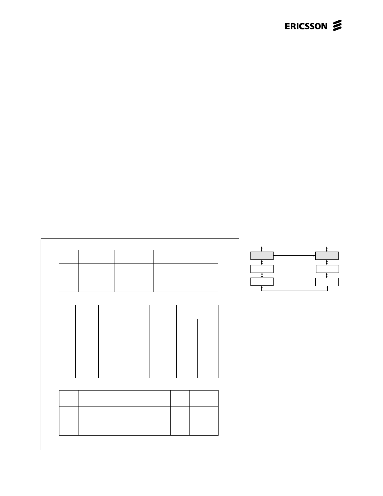
Table 1: Link Control Packets Table, ACL Packets Table, SCO packets
Figure 13. Link manager
filter-out the message and does not
need to acknowledge the message
to the transmitting LM due to the
reliable link provided by the
Baseband and radio.
LM to LM communication can take
place without actions taken by the
host. Discovery of features at other
Bluetooth enabled devices nearby
can be found and saved for later use
by the host.
Please refer to the Specification of
the Bluetooth System v1.0B part C
for in-depth information regarding
the LMP.
Page 13
ROK 101 007
13
Preliminary
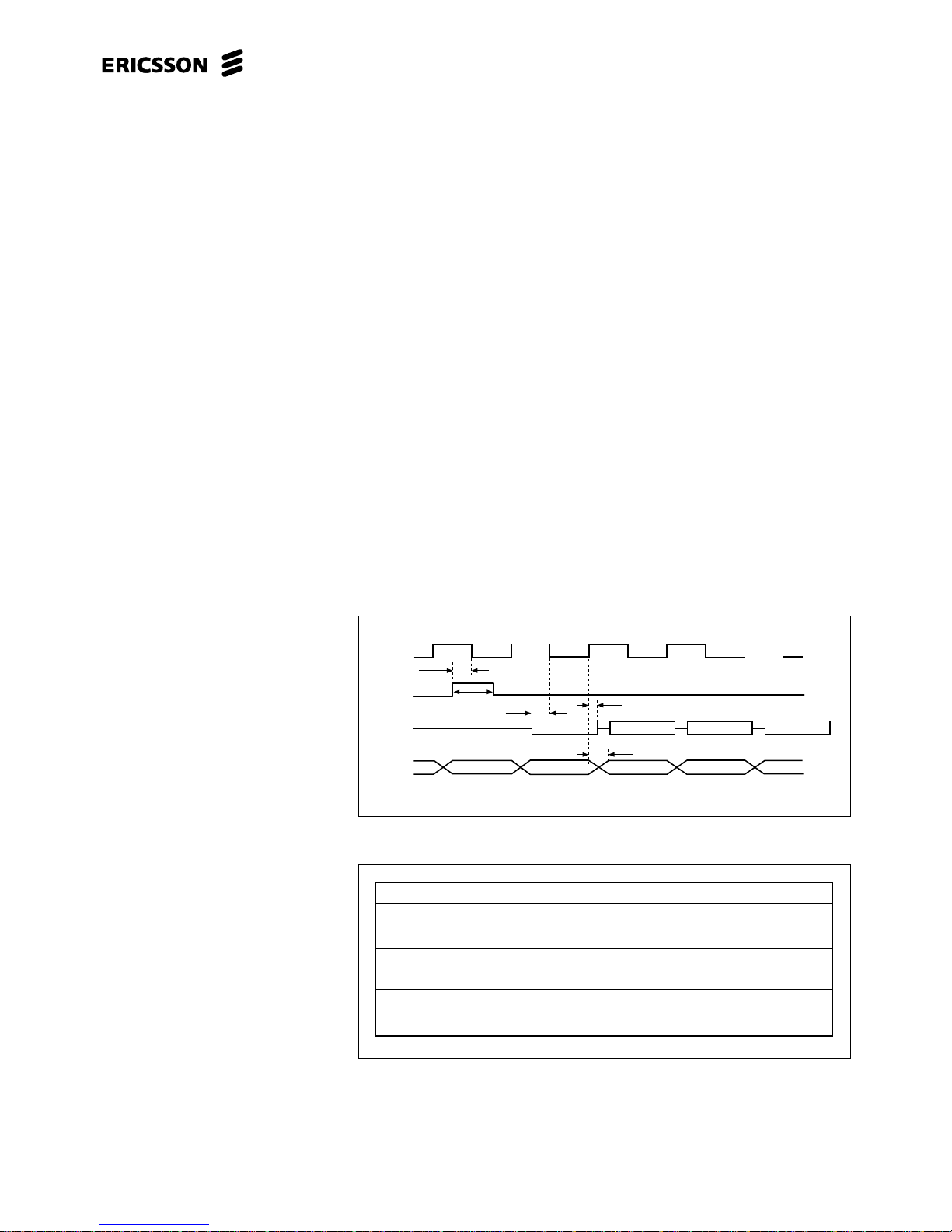
Figure 14. PCM timing
Table 2. PCM parameters
Host Control Interface (HCI)
The HCI provides a uniform command I/F to the Baseband and Link
Manager and also to HW status
registers.
There are three different types of HCI
packets:
• HCI command packets – from
host to Bluetooth module HCI.
• HCI event packets – from
Bluetooth module HCI to host.
• HCI data packets – going both
ways.
It is not necessary to make use of all
different commands and events for
an application. If the application is
aimed at a pre-specified profile, the
capabilities of such a profile is
necessary to adjust to – see Specification of the Bluetooth System v1.0B
Profiles.
a) With the HCI UART Transport
Layer on top of HCI, the module
will communicate with a host
through the UART I/F. The PCM I/
F is also available for communicating voice.
b) With the HCI USB Transport
Layer on top of the HCI, the
module will communicate with a
host through the USB. Detach
and Wake_up signals are also
available for notebook implementations.
Please refer to the Specification of
the Bluetooth System v1.0B part H:14 for in-depth information regarding
the HCI and different transport layers
Module HW Interfaces
UART Interface
The UART implemented on the
module is an industry standard
16C450 and supports the following
baud rates: 300, 600, 900, 1200,
1800, 2400, 4800, 9600, 19200,
38400, 57600, 115200, 230400 and
460800 bits/s. 128 byte FIFOs are
associated with the UART.
Four signals will be provided for the
UART interface. TxD & RxD are used
for data flow, and RTS & CTS is used
for flow control.
Please refer to the Specification of
the Bluetooth System v1.0B part H:4
regarding the HCI and UART transport layers.
PCM Voice Interface
The standard PCM interface has a
sample rate of 8 kHz (PCM_SYNC).
The PCM clock is variable between
200 kHz and 2.0MHz. The PCM data
can be linear PCM (13-16bit), µ-Law
(8bit) or A-Law (8bit).
The PCM I/F can be either master or
slave – providing or receiving the
PCM_SYNC. Redirection of
PCM_OUT and PCM_IN can be
accomplished as well.
Over the air the encoding is programmable to be CVSD, A-Law or µ-Law.
Preferably the robust CVSD encoding
should be used.
USB Interface
The module is a USB high-speed
class device (12Mbps) that has the
full functionality of a USB slave and
is compliant to the USB 1.1 specification. Data transfer occurs on the
bi-directional ports, D+ & D-.
Additionally, there are two side band
signals for a notebook application.
Two side band signals Wake_up and
Detach are used to control the state
from which the notebook resumes.
When the host is in a power down
mode, Wake_up wakes the host up
when the Bluetooth system receives
an incoming connection. The host
indicates that it is in Suspend mode
by using the Detach signal.
I2C Interface
A master I2C I/F is available on the
module. The control of the I2C pins
are performed by Ericsson specific
HCI commands available in the FW
implementation – see Appendix C.
MSB MSB-1 MSB-2
PCM_CLK
PCM_SYNC
PCM_X in
PCM_X out
t
PSS
t
PSH
t
DSL
t
DSH
t
PDLP
MSB MSB-1 MSB-3MSB-2
Name Description Min Typ Max Unit
f
pcmClk
PCM data-transfer clock frequency 1 128 2000 kHz
f
pcmSync
PCM sample rate sync. frequency 8 kHz
t
CCH
PCM_CLK high period 200 ns
t
CCL
PCM_CLK low period 200 ns
t
PSS
PCM_SYNC (setup) to PCM CLK (fall) 100 ns
t
PSH
PCM_SYNC pulse length 200 ns
t
DSL
PCM_X in (setup) to PCM_CLK (fall) 100 ns
t
DSH
PCM_X in (hold) from PCM_CLK (fall) 100 ns
t
PDLP
PCM_X out valid from PCM_CLK (rise) 150 ns
Page 14
ROK 101 007
14
Preliminary
Antenna
The ANT pin should be connected to
a 50Ω-antenna interface, thereby
supporting the best signal strength
performance. Ericsson Microelectronics can recommend application
specific antennas – see Appendix C.
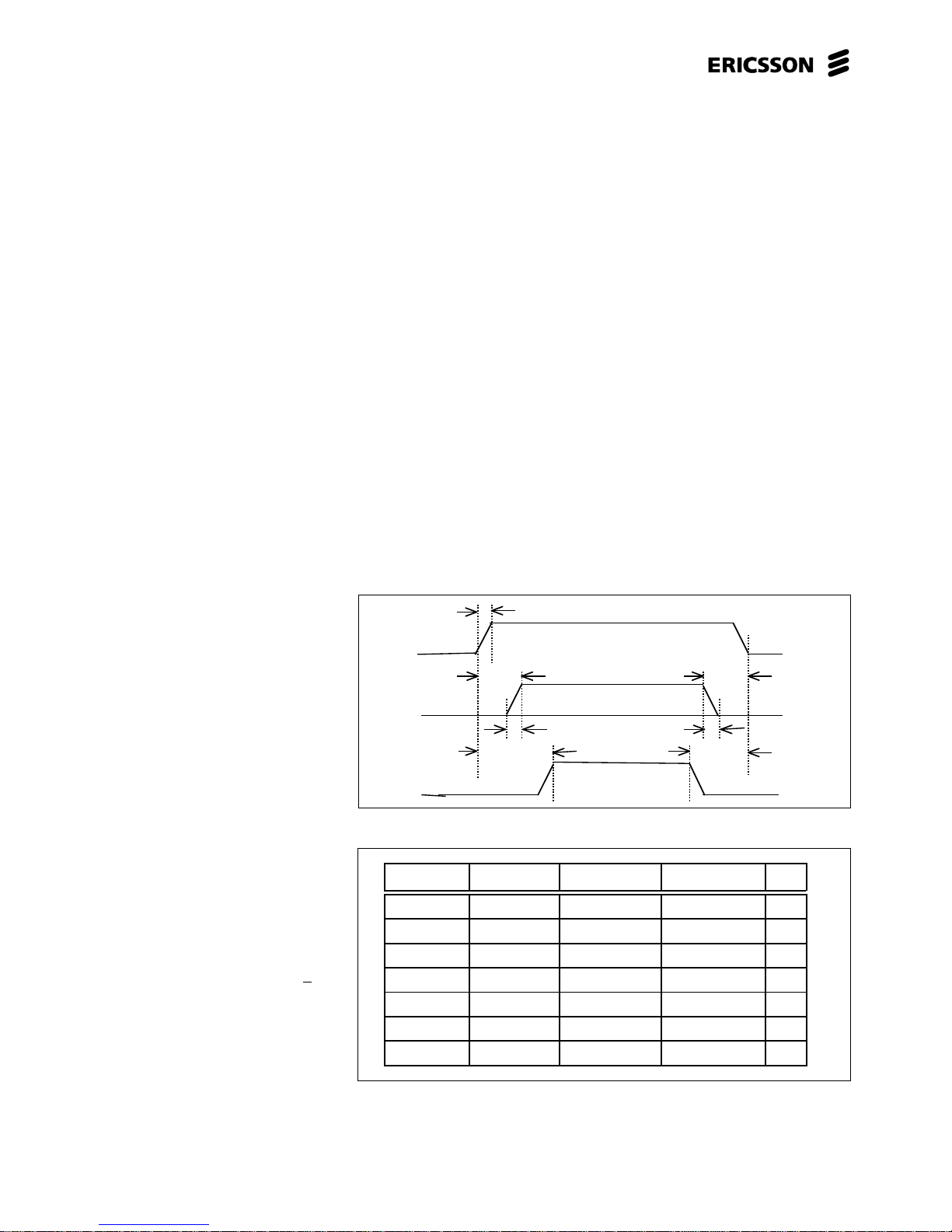
Power-up Sequence
There is no need for a power up
sequence if VCC, ON and VCC_IO
are tied together.
A power up sequence, if used, shall
be applied accordingly: Connection
of the supply rails, GND and then
V
CC
; then the ON signal should be
applied in order to initiate the internal
regulators; and finally, the VCC_
IO
supply rail can be activated.
The power-down sequence is similar
to the power-up procedure but in the
reverse format. Therefore, the
disconnection of the signals shall be
as follows: VCC_IO, ON,VCC and finally
GND.
RESET#
The assignment of the RESET# input
is to generate a reset signal to the
complete Bluetooth module. During
power-up the reset signal is set ‘low’
automatically so that power supply
glitches are avoided. Therefore no
reset input should be required after
power-up.
When implementing an external
RESET#, the signal should be fed
from an open drain output.
Power
There are three inputs to the Voltage
Management section (VCC, V
CC_IO
,
ON). VCC is the supply voltage that is
typically 3.3V.
A separate power supply rail (V
CC_IO
)
is provided for the I/O ports, UART,
PCM and USB. To be compliant with
the USB 1.1 specification, V
CC_IO
>
3.11V. V
CC_IO
can either be connected
to VCC or to a dedicated supply rail,
which is the same as the logical
interface of the host.
VCC
ON
VCC_IO
t
d_VCC_IO_o
t
d_VCC_IO_o
t
d_off
t
d_on
t
r
t
r_on
t
f_on
Parameter Min Nom Max Unit
t
r
1 ms
t
r_on
60 µs
t
f_on
60 µs
t
d_on
t
r
µs
t
d_off
µs
t
dvcc_io_on
t
d_on
µs
t
dvcc_io_off
t
d_off
µs
Figure 15. Power up sequence
Table 3. Power up parameters
Shielding / EMC Requirements
The module has its own RF shielding
and is approved according to the
standards by FCC and ETSI.
If the approval number is not visible
on the outside when the module is
utilized in the final product, an
exterior label must state that there is
a transmitter module inside the
product.
Ground
Ground should be distributed with
very low impedance as a ground
plane. Connect all GND pins to the
ground plane.
Assembly Guidelines
Solder Paste
The ROK 101 007 module is made
for surface mounting and the SSP
connection pads have been formed
after printing eutectic Tin/Lead solder
paste. The solder paste to use is not
critical as long as this is a normal
eutectic solder paste. A preferred
solder paste height is 150µm.
Soldering Profile
It must be noted that the module
should not be allowed to be hanging
upside down in the re-flow operation.
This means that the module has to
be assembled on the side of the PCB
that is soldered last.
The re-flow process should be a
regular surface mount soldering
profile (full convection strongly
preferred); the ramp-up should not
be higher than 2
o
C/s and with a peak
temperature of 210-235oC during 2060 seconds.
Pad Size
It is recommended that the pads on
the PCB should have a diameter of
0.7-0.9 mm. The surface finish on the
PCB pads should be Nickel/Gold or a
flat Tin/Lead surface or OSP (Organic
Surface Protection).
Page 15

ROK 101 007
15
Preliminary
Placement
The placement machine should be
able to recognize odd BGA combinations (all ball recognition preferred)
and be able to pick the component
asymmetrical. The module contains a
flat pick-area of 10mm diameter
minimum. The weight of the module
is typically 2.8gr.
Storage
Keep the component in its dry pack
when not yet using the reel. After
removal from the dry pack ensure
that the modules are soldered onto
the PCB within 48 hours.
Marking
Every module is marked with the
following information on the:
a) Component designation: “ROK
101 007”.
b) Ericsson’s name and logotype.
c) Manufacturing code (place, year,
week) and batch number.
d) CE logotype
e) Type approval RTA no. See
manual
Ordering Information
Package Part No.
30 GP ROK 101 007/1
30 SSP ROK 101 007/2
Packaging
All devices will be delivered in a
package protecting them from
electrostatic discharges and mechanical shock. The package will be
marked with the following information:
a) Delivery address.
b) Purchase order-number
c) Type of goods and component
designation.
d) Ericsson’s name and logotype.
e) Date of manufacture and batch
number.
f) Number of components in the
package.
Microelectronics
Ericsson Microelectronics AB
SE-164 81 Kista-Stockholm, Sweden
Telephone: +46 8 757 50 00
www.ericsson.com/microe
1522-ROK 101 007 Rev. PA5
© Ericsson Microelectronics AB, April 2000
Information given in this data sheet is believed
to be accurate and reliable. However no
responsibility is assumed for the consequences
of its use nor for any infringement of patents or
other rights of third parties which may result
from its use. No license is granted by
implication or otherwise under any patent or
patent rights of Ericsson Microelectronics.
These products are sold only according to
Ericsson Microelectronics' general conditions of
sale, unless otherwise confirmed in writing.
Specifications subject to change
without notice.
Abbreviations
ASIC - Application Specific
Integrated Circuit
BER - Bit Error Rate
CMOS - Complementary Metal Oxide
Semiconductor
C/I - Carrier to Interference Ratio
DCE - Data Circuit terminating
Equipment
GP - Gold Print
HCI - Host Controller Interface
ISM - Industrial Scientific and
Medical
PCB - Printed Circuit Board
PCM - Pulse Code Modulation
PDA - Personal Digital Assistant
PtP - Point to Point
Rx - Receive
SIG - Special Interest Group
SSP - Screen Solder Print
Tx - Transmit
UART - Universal Asynchronous
Receiver Transmitter
USB - Universal Serial Bus
VCO - Voltage Controlled Oscillator
Page 16
ROK 101 007
16
Preliminary
APPENDIX A
Getting Started
The ROK 101 007 Bluetooth module
is easy to use when designing a
Bluetooth application. However,
there is a need for know-how in the
Bluetooth System specification v1.0B
as well as the Profile specification
v1.0B when designing and endcustomer product.
• Bluetooth module
• Know-how in Bluetooth specifica-
tion regarding HCI commands
• Test board with UART/PCM or
USB I/F
• Visual C++ for PC SW design
• Preferably HCIdriver, L2CAP,
RFCOMM and SDP from Ericsson
The list above show some parts that
would make designing convenient.
All information needed, regarding
how to drive the HCI over UART is
specified in part H4 of the Bluetooth
System v1.0B further more part H1
and also Appendix IX with message
charts is relevant.
Below follow an example of how to
set up an ACL link between to
Bluetooth modules by using the
UART I/F and also a schematic of
how to interface the module and
control it by a host, normally a PC or
microcontroller.
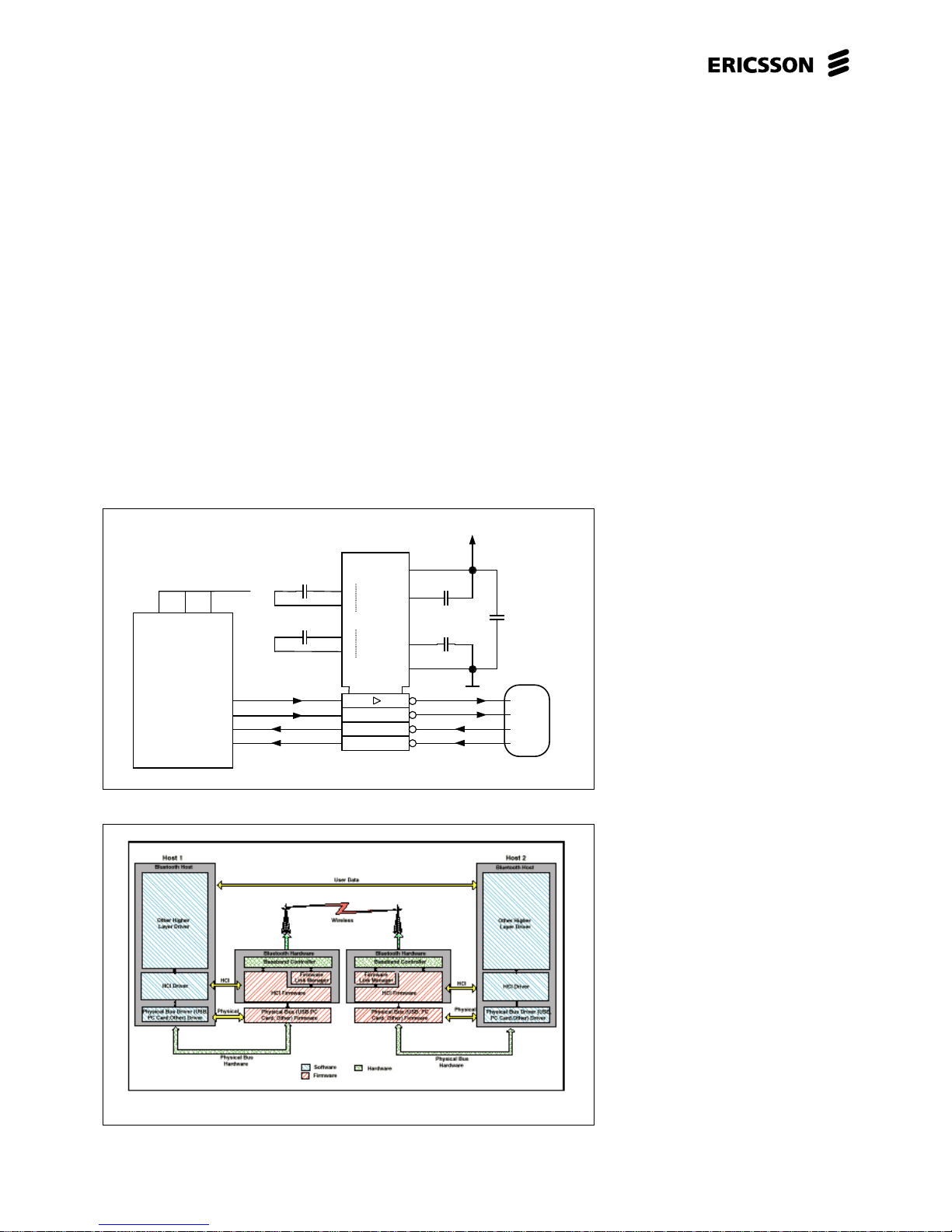
Principle schematic for
UART inter- connect
The inter-connection to the levelshifter when designing a test-board
could be according to the schematic
below. (Figure A1.)
The Bluetooth module can be
connected as a DCE/DTE and a
modem/nullmodem cable could
therefor be used in-between the testboard and the PC.
Setting up a Bluetooth
point-to-point connection
The Host Controller Interface (HCI) in
the module is a command I/F. The
host presents commands to the HCI
and receives events back from the
HCI of the module. The module Link
Manager provides link set up capability to the HCI.
• Host_B Bluetooth module is set in
paging scan mode – listening for
a Bluetooth device asking for a
new connection
• Host_A Bluetooth module is set in
paging mode asking for a connection to Host_B
This is accomplished by first setting
up the connection between the Host
and the module and thereafter
creating the connection between the
modules using HCI commands.
V+
MAX3232E
V-
+
-
RS-232
+
-
CX
CX
10
11
9
12
100nF
100nF
1
3
4
5
2
6
100nF
100nF
V
CC
7
14
8
13
9-pin D-sub
2 RXD
8 CTS
3 TXD
7 RTS
BLUETOOTH
MODULE
ROK 101 007
B5
B6
A5
A6
TXD
CTS
RXD
RTS
16
V
CC
15
GND
100nF
The capacitor values are
chosen for a VCC from
3.2 to 3.6 V
V
CC
VCC VCC_IO ON
Figure A1. Bluetooth module connected as a DCE through level shifter
Figure A2. Bluetooth host to host communication
Page 17
ROK 101 007
17
Preliminary
Host set-up via UART:
There are 4 different types of HCIpackets accepted on the UART I/F.
• Read_Buffer_Size: Providing the
host with information on buffer
size for ACL and SCO data
packets for the module returned
with a
Command_Complete_Event
packet. The host shall use this
information for controlling the
transmission
• Host_Buffer_Size: Providing the
module with information on buffer
size for ACL and SCO packets to
the host.
It is the host that manages the data
buffers of the Host Controller on the
module.
Timers
It could be necessary to set important timers used by the module for
time out handling. The timers are all
set by writing to registers using HCI
commands.
The default values can be checked in
Specification of the Bluetooth
System v1.0B part H:1 or by using
Read_xxx_xxx commands.
Bluetooth Address
The hosts, using the HCI command
Read_BD_ADDR will find the
Bluetooth address of the module by
the Command_Complete_Event with
the BD_ADDR as a parameter.
By Remote_Name_Request, the
BD_ADDR of the remote module can
also be found.
Inquiry
The HCI command Inquiry with the
parameters LAP, Inquiry_Length, and
Num_Responses can also be used
for collecting BD_ADDR of remote
Bluetooth units.
Creating a Point-to-point
connection
Page Scan mode
HCI packet type HCI packet indicator
HCI command packet 0x01
HCI ACL data packet 0x02
HCI SCO data packet 0x03
HCI event packet 0x04
The HCI packet indicator shall be
sent immediately before the HCI
packet. When the entire HCI packet
has been received a new indicator
should be expected.
The default speed setting is 57.6 kb/s
and can be changed by sending a
specified bit stream to the I/F - see
Appendix C on how to change the
speed setting of the UART.
When the speed set-up for the UART
is made for both Host_ A & B, the
Command Packets can be sent and
Event Packets received by the hosts.
See HCI over UART in part H:4 of the
Bluetooth System v1.0B for detailed
information regarding parameters
and protocol.
Soft Reset
First HCI command packet to send
should be the RESET packet.
A Command_Complete_Event with a
status parameter should be returned
to the host.
Buffer information
Buffer information should be exchanged between the module and
respective host by using HCI commands.
Command Return
Command OCF parameters parameters
HCI_Write_Scan_Enable 0x0005 Scan_Enable Status
To set a Bluetooth module in the
mode for being able to connect to
(Host_B), page scan mode, there are
some settings that should be performed.
The Write_Scan_Enable command
with correct parameter
(Scan_Enable=0x001A) will set the
module in Page scan mode if the
Command_Complete_Event is
successful.
Furthermore the setting of authentication and encryption should be
disabled (default) by using the:
• Write_Authentication_Enable
• Write_Encryption_Mode
The basic settings for getting into
scan mode could be according to the
below suggested script list.
• Read Buffer Size
• Set Event Filter
• Write Scan Enable: (Scan Enable:
0x03)
• Write Voice Setting: (Voice
Channel Setting: 0x0060)
• Write Authentication Enable:
(Authentication Enable: 0x00)
Table A1. HCI packets
Table A2. HCI Write Scan Enable
OCF code
Page 18
ROK 101 007
18
Preliminary
• Set Event Filter: (Connection
Setup Filter: Connections from All
Devices, Auto Accept: 0x02)
• Write Connection Accept
ACL link up and running
Host_A is the master of the point-topoint piconet and Host_B is slave.
The unit starting the paging process
is by definition the master. The link
set-up is completed when the event
Connection_Complete_Event is
returned to both Host_A and Host_B
with the connection handle as one of
the parameters and the status
parameter 0x00 (success). When
Bluetooth link is up and running the
HCI data packets can be sent from
host to host.
The host must take care of generating the packages going from Host to
Host Controller in the module over
the UART I/F, in the same way the
Host must arrange the packages
received from the Host Controller.
Both sides need information on what
kind of data is received, to be able to
interpret the bit flow correctly.
For extensive information on setting
up a Bluetooth link please refer to
Bluetooth System v1.0B Appendix IX
Message Sequence Charts
Adding an SCO link
When creating a voice connection
using the PCM I/F, an ACL link must
be up and running between the two
devices, an SCO link can thereafter
be added.
The control of the PCM I/F (FS,
PCM_IN/OUT and PCM_CLK) is
handled by Ericsson specific HCI
command – see Appendix C.
Driving SW
HCI- API
The Bluetooth module includes all
HCI command capabilities according
to Bluetooth System v1.0B. Furthermore, there is some Ericsson specific
commands available for accessing
HW registers and HW control – see
Appendix C. SW for driving the
module should be developed for the
HCI interface.
There is source code SW available
with Ericsson Bluetooth Developers
Kit (EBDK), see Appendix B, which
can be used for driving the module.
This SW comes with the EBDK and
has an HCI-API for application
development on the HCI I/F.
Higher layer-API
Software (HCIdriver, L2CAP,
RFCOMM and SDP) are available in a
generic, source code format, i.e. to
be adapted to various operating
systems.
• HCIdriver – implements the HCI
command driver used by the host
• L2CAP – handles protocol
multiplexing, segmentation and
re-assembly of packets
• RFCOMM – provides a serial port
emulation over the L2CAP
protocol
• SDP – Service Discovery Protocol
provides information on the
services available on a Bluetooth
device
Additional SW for the application
shall be developed for the actual
application on top of the RFCOMM
API. If the application is according to
a SIG predefined profile, it should be
implemented accordingly. New
applications can be the driver of the
specification of new profiles decided
by the SIG – see Specification of the
Bluetooth System v1.0B Profiles.
0481216202432
Connection handle PB BC Data total length
Flag Flag
Data
Timeout: (Connection Accept
Timeout: 0x2000)
• Write Page Timeout: (Page
Timeout: 0x3000)
Page mode
The Create_Connection command is
used to set-up a link to another
Bluetooth device.
Create_Connection:
BD_ADDR: 0xYYYYYYYYYYYY,
Packet Type: 0x0007,
Page Scan Repetition Mode: 0x01,
Page Scan Mode: 0x00, Clock
Offset: 0x0000
This command will cause the Link
Manager to try to create a connection to the Bluetooth module with the
appropriate BD_ADDR. The local
Bluetooth module (Host_A) starts the
paging process to set up a link to the
page-scanning remote device
(Host_B).
By LMP the negotiation between the
two Bluetooth modules Link Managers (LM) the link set-up can be
completed.
Return
Command OCF Command parameters parameters
HCI_Create_Connection 0x0005 BD_ADDR
Packet_Type
Packet_Scan_Repetition_Mode
Packet_Scan_Mode
Clock_Offset
Table A3. HCI Create Connection
OCF code
Table A4. ACL data packet
Page 19
ROK 101 007
19
Preliminary
APPENDIX B
Development tools
Ericsson Bluetooth Development
Kit (EBDK)
The easiest way of getting started is
to use the Ericsson Bluetooth
Developers Kit. It provides all parts
necessary for developing applications for the Bluetooth module.
Available are:
• PC plug&play
• Demos using radio/baseband
• Macro capability
• C++ v5.0 Source code for use in
applications
• HCIdriver, L2CAP, SDP and
RFCOMM for applications using
UART communication
• Pins for electrical measurements
• Antennas
Development can easily take place
on the EBDK platform and thereafter
the implementation of the full
Bluetooth capability can be setup by
developed SW/HW and the Bluetooth
module.
Software (HCIdriver, L2CAP,
RFCOMM and SDP) will be available
in source code for PC.
• HCIdriver – implements the HCI
command driver used by the host
• L2CAP – handles protocol
multiplexing, segmentation and
re-assembly of packets
• RFCOMM – provides a serial port
emulation over the L2CAP
protocol
• SDP – Service Discovery Protocol
provides information on the
services available on a Bluetooth
device
Technical support is available from
the EBDK distributor. Please contact
Ericsson Microelectronics for ordering and information regarding the
EBDK and regarding extra daughter
board with ROK 101 007 as add-on
to the EBDK.
Ericsson Bluetooth Starter Kit (EBSK)
A very small convenient kit, which
preferably is used in point-tomultipoint configuration designs,
based on the Bluetooth module ROK
101 007.
Please contact Ericsson Microelectronics for ordering and information
regarding the Ericsson Bluetooth
Starter Kit.
Base Band Board
Application Board
Radio Board
JTAG
I2C
Audio
USB
Monitoring pins
RS-232 RS-232 RS-232
Ericsson BaseBand
Ericsson Radio
Module
Address / Data / Control
USB9602 MS7540
Radio Board (0dBm)
Ericsson Radio
Module
Radio Board (20dB m)
Ericsson Radio
Module
optional external antenna
GLUE LOGIC (XLINX)
LEDS
Memor y
Memory
EBDK
A
udioRS-232 USB
Ericsson Bluetooth
Module ROK 101 007/1
Codec
Power
DC/DC
Level-
shift
EBSK
Figure B1. Ericsson Bluetooth Development Kit (EBDK)
Figure B2. Ericsson Bluetooth Starter Kit (EBSK)
Page 20
ROK 101 007
20
Preliminary
APPENDIX C
Bluetooth Information
This part will be updated and new
information will be added continuously.
Radio
Fast Frequency hopping (1600channel hop/s) with 79(23) channels
available (2.402 to 2.480 GHz) and a
symbol rate of 1Ms/s over the air
exploits the maximum channel
bandwidth in the unlicensed ISM
band.
To sustain a high transfer rate in busy
radio environment, the frequency
hopping together with advanced
coding techniques maximizes the
throughput.
During Page and Inquiry the hopping
frequency is risen to 3200 hops/s to
enhance the time needed for connection set-up.
Modulation technique is a binary
Gaussian Frequency Shift Keying
GFSK, with a BT product of 0.5. The
channel bandwidth is 1 MHz and the
frequency deviation from the carrier
frequency of the RF channel is
between +/-140 to +/-175 kHz for
representing a ‘1’/’0’.
A rapid process is ongoing to
harmonise Spanish, French and
Japanese frequency ranges with the
rest of the world.
Data and parameter formats
There are exceptions in the Bluetooth
system for data and parameter
formats – general rules below.
• All values are in Binary and
Hexadecimal little Endian formats
• Negative values must use 2’s
Country Frequency range RF channels
Europe & USA 2400-2483.5 MHz f = 2402 + k MHz k = 0....78
Japan 2471-2497 MHz f = 2473 + k MHz k = 0....22
Spain 2445-2475 MHz f = 2449 + k MHz k = 0....22
France 2446.5-2483.5 MHz f = 2454 + k MHz k = 0....22
Table C1. Frequency ranges used.
complement format
• Array parameter notation is
parameterA[i], parameterB[i],…
• All
parameter values are sent/received in
little Endian format. The least significant byte is sent first – unless noted
otherwise.
HCI Opcodes
The Opcodes have been changed
during the ongoing standardisation
work. Below is the description on
how to send opcodes to the module.
Below is the general HCI command
HCI_Inquiry_Cancel (Example):
OGF: 0x01
bin: 0000 0001
OCF: 0x0002
bin: 0000 0000 0000 0010
Real code bin: 0000 01 | 00 0000 0010
LINK CONTROL COMMAND
0 x 0 4 0 2
Sent to module in hex: 02 04 00
Reverse byte order
Zero parameters
lsb lsbmsbmsb
msb lsb
OpCode
OCF OGF
Parameter
Total length
OpCode Command
Field
10 bits
OpCode Group
Field
6 bits
Little
Endian
OGFRange (6 bits): 0x00-0x3F 0x3E: Bluetooth logo testing
0x3F: Vendor specific debug commands
OCFRange (10 bits): 0x0000-0x03FF
Amount of parameters in bytes
msb msblsblsb
0@ 4@ 8@ 12@ 16@ 20@ 24@ 28@ 31
Figure C1. Byte order sent to module
Page 21
ROK 101 007
21
Preliminary
UART speed
460.8 kbps
230.4 kbps
115.2 kbps
57.6 kbps
28.8 kbps
14.4 kbps
7200 bps
3600 bps
1800 bps
900 bps
153.6 kbps
76.8 kbps
38.4 kbps
19.2 kbps
9600 bps
4800 bps
2400 bps
1200 bps
600 bps
300 bps
Parameter to send
00000
00001
00010
00011
00100
00101
00110
00111
01000
01001
10000
10001
10010
10011
10100
10101
10110
10111
11000
11001
Table C2. UART speed setting parameter
packet format depicted as well as a
byte order description.
UART speed setting
The baud rate is changed with an
Ericsson specific HCI command.
HCI_Ericsson_Set_Uart_Baud_Rate
The command has one parameter,
baud rate - one byte long according
to the table below . The op-code for
the command is 0xfc07 - the last
figure is due to a possible change.
Sending the command should be
performed accordingly: 07 fc 01 yz ,
where yz is the chosen baud rate
from the table.
The op-code is sent in reverse byte
order. 01 is the parameter length, in
this case one byte. Remember to add
the HCI packet indicator.
Observe - When changing the baud
rate for the module the host also has
to change the baud rate.
Observe - Removing power to the
module the baud rate will be reset to
57.6 kbps.
Observe -Two zeros are not printed
in the beginning of the binary parameters below. The length of the
parameter is 1 byte.
Ericsson specific HCI commands
By using the Ericsson specific HCI
command there are a number of
features available for the application
design.
Contact Ericsson Microelectronics
for a command reference list.
Antennas
Antenna design is not specified and
standardised in the Bluetooth System
v1.0B.
Many different types of antennas can
and will be used. Application specific
antennas suitable for production are
expected to be a new market for
antenna designs.
Ericsson Microelectronics have
antennas for the EBDK and other
development kits. Contact Ericsson
Microelectronics for information on
antennas.
Contacting Ericsson
Microelectronics
For further information regarding
Bluetooth technology, components
and development tools, please
contact Ericsson Microelectronics:
Telephone:
Scandinavia: +46 8 757 47 00
Europe: +44 1793 488 300
North America: +1 877 374 26 42
Rest of World: +46 8 757 47 00
www.ericsson.se/microe
 Loading...