

Ericsson PTF10021 Datasheet
PTF 10021
30 Watts, 1.4–1.6 GHz
GOLDMOS
™
Field Effect Transistor
Description
The PTF 10021 is an internally matched common source N-channel
enhancement-mode lateral MOSFET intended for linear driver and
final applications in the 1.4 to 1.6 GHz range such as DAB/DAR. It is
rated at 30 watts power output. Nitride surface passivation and full
gold metallization ensure excellent device lifetime and reliability.
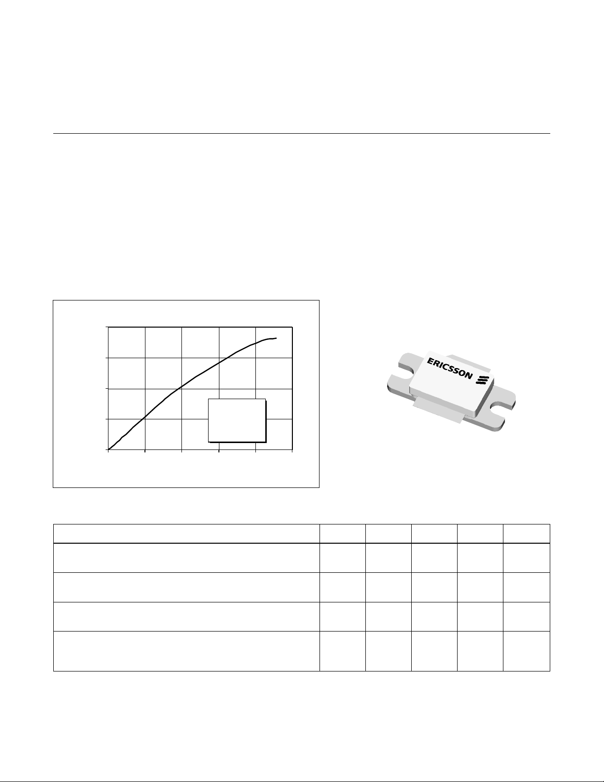
Typical Output Power vs. Input Power
40
30
20
INTERNALLY MATCHED
•
• Performance at 1.5 GHz, 28 Volts
- Output Power = 30 Watts Min
- Power Gain = 13 dB Typ
- Efficiency = 48% Typ
• Full Gold Metallization
• Silicon Nitride Passivated
• Excellent Thermal Stability
• 100% Lot Traceability
10021
A-1234569813
VDD = 28 V
10
Output Power (Watts)
0
012345
Input Power (Wa tts)
I
= 360 mA
DQ
f = 1.5 GHz
Package 20237
RF Specifications (100% Tested)
Characteristic Symbol Min Typ Max Units
Gain
(V
Power Output at 1 dB Compressed
(V
Drain Efficiency
(V
Load Mismatch Tolerance
(V
all phase angles at frequency of test)
All published data at T
= 28 V, P
DD
= 28 V, P
DD
= 28 V, P
DD
= 28 V, P
DD
= 10 W, IDQ = 360 mA, f = 1.5 GHz) G
OUT
= 30 W, IDQ = 360 mA, f = 1.5 GHz) P-1dB 30 — — Watts
OUT
= 30 W, IDQ = 360 mA, f = 1.5 GHz) h 45 48 — %
OUT
= 30 W(PEP), IDQ = 360 mA, f = 1.5 GHz— Y — — 10:1 —
OUT
= 25°C unless otherwise indicated.
CASE
ps
11.0 13.0 — dB
e
1

PTF 10021
y
y
)
)
e
Electrical Characteristics (100% Tested)
Characteristic Conditions Symbol Min Typ Max Units
Drain-Source Breakdown Voltage VGS = 0 V, ID = 25 mA V
(BR)DSS
Drain-Source Leakage Current VDS = 28 V, VGS = 0 V I
Gate Threshold Voltage VDS = 10 V, ID = 75 mA V
Forward Transconductance VDS = 10 V, ID = 3 A g
DSS
GS(th)
fs
65 — — Volts
— — 1.0 mA
3.0 — 5.0 Volts
— 2.2 — Siemens
Maximum Ratings
Parameter Symbol Value Unit
Drain-Source Voltage V
Gate-Source Voltage V
Operating Junction Temperature T
Total Device Dissipation at P
DSS
GS
J
D
Above 25°C derate by 0.6 W/°C
Storage Temperature Range T
Thermal Resistance (T
= 70°C) R
CASE
STG
qJC
65 Vdc
±20 Vdc
200 °C
105 Watts
–40 to +150 °C
1.65 °C/W
Typical Performance
Typical P
15
14
13
Gain
12
Gain (dB)
11
10
1300 1400 1500 1600 1700
, Gain & E fficiency
OUT
vs. Frequenc
Outp ut P owe r (W)
VDD = 28 V
= 360 mA
I
DQ
Frequency (MHz)
(at P-1dB)
Efficiency (%)
Broadband Test Fixture Performance
60
50
40
30
20
Output Power & Efficienc
10
14
12
10
8
Gain (dB)
6
4
1400 1450 1500 1550 1600
Gain (dB)
VDD = 28 V
= 360 mA
I
DQ
= 10 W
P
OUT
Frequency (MHz)
Efficiency (%)
Return Loss (dB)
60
50
40
Efficiency (%
- 5
30
-15
20
-25
10
-35
0
Return Loss (dB
2
 Loading...