

Ericsson PTF10020 Datasheet

PTF 10020
)
125 Watts, 860–960 MHz
GOLDMOS
™
Field Effect Transistor
Description
The PTF 10020 is an internally matched, 125 Watt LDMOS FET
intended for large signal amplifier applications from 860 to 960 MHz.
Nitride surface passivation and gold metallization ensure excellent
device lifetime and reliability.
Typical Output Pow er vs. Input Pow er
150
125
100
75
50
25
Output Power (Watts
0
01234567
960 MHz
900 MHz
860 MHz
Input Power (Watts)
VDD = 28 V
= 1.4 A Total
I
DQ
INTERNALLY MATCHED
•
• Performance at 960 MHz, 28 Volts
- Output Power = 125 Watts
- Power Gain = 12.5 dB Typ
- Efficiency = 55% Typ
• Full Gold Metallization
• Silicon Nitride Passivated
• Back Side Common Source
• 100% Lot Traceability
10020
A-1234569813
Package 20240
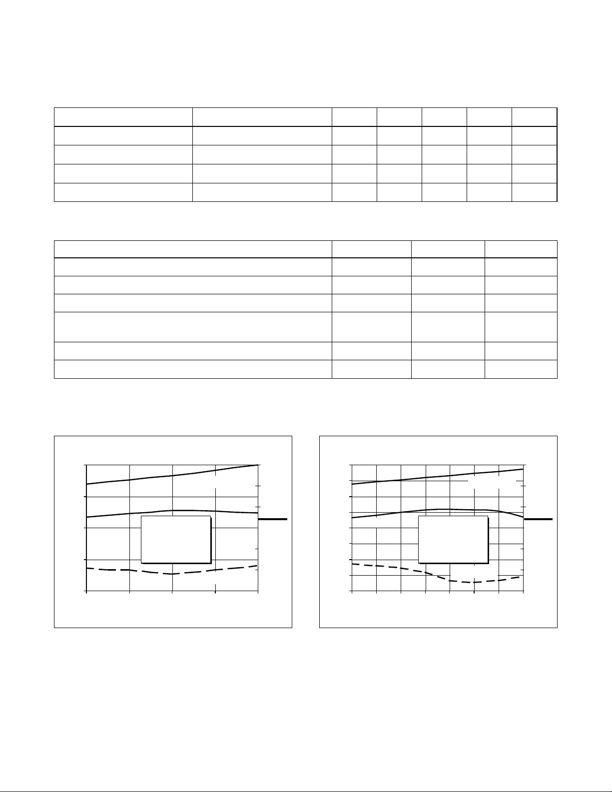
RF Specifications (100% T ested)
Characteristic Symbol Min T yp Max Units
Gain
(V
Power Output at 1 dB Compression
(V
Drain Efficiency
(V
Load Mismatch Tolerance
(V
f = 959.9, 960 MHz—all phase angles at frequency of test)
All published data at T
= 28 V , P
DD
= 28 V , ICQ = 1.4 A T otal, f = 960 MHz) P-1dB 125 130 — Watts
DD
= 28 V , P
DD
= 28 V , P
DD
= 125 W, IDQ = 1.4 A Total, f = 960 MHz) G
OUT
= 125 W, IDQ = 1.4 A Total, f = 960 MHz) h 50 55 — %
OUT
= 125 W(PEP), IDQ = 1.4 A T otal, Y — — 10:1 —
OUT
= 25°C unless otherwise indicated.
CASE
ps
11.0 12.5 — dB
e
1
PTF 10020
)
y
)
y
e
Electrical Characteristics (100% Tested—characteristics, conditions and limits shown per side)
Characteristic Conditions Symbol Min Typ Max Units
Drain-Source Breakdown Voltage VGS = 0 V , ID = 5 mA V
(BR)DSS
Drain-Source Leakage Current VDS = 28 V , VGS = 0 V I
Gate Threshold Voltage VDS = 10 V , ID = 75 mA V
Forward Transconductance VDS = 10 V , ID = 3 A g
DSS
GS(th)
fs
65 — — Volts
— — 1.0 mA
3.0 4.3 5.0 Volts
— 2 .5 — Siemens
Maximum Ratings
Parameter Symbol Value Unit
Drain-Source Voltage
Gate-Source Voltage
Operating Junction T emperature T
T otal Device Dissipation at P
Above 25°C derate by 1.67 W/°C
Storage T emperature Range T
Thermal Resistance (T
(1)
per side
(1)
(1)
= 70°C) R
CASE
V
V
DSS
GS
J
D
STG
qJC
65 Vdc
±20 Vdc
200 °C
290 Watts
–40 to +150 °C
0.6 °C/W
Typical Performance
Broadband Test Fixtur e Performance
20
Efficiency %
16
Gain
12
Gain (dB)
8
4
860 870 880 890 900
VDD = 28 V
= 1.4 A Tota l
I
DQ
= 125 W
P
OUT
Return Loss
Frequency (MHz)
60
50
Efficienc
40
- 5
30
-15
20
-25
10
-35
0
Return Loss (dB
Broadband Test Fixtur e Performance
20
18
16
14
Gain
12
Gain (dB)
10
8
6
4
925 930 935 940 945 950 955 960
VDD = 28 V
= 1.4 A Tota l
I
DQ
P
OUT
Frequency (MHz)
Efficiency %
= 125 W
Return Loss
60
50
Efficienc
40
- 5
30
-15
20
-25
10
-35
0
Return Loss (dB
2
 Loading...