

Ericsson PTF10019 Datasheet

PTF 10019
r
70 Watts, 860–960 MHz
GOLDMOS
™
Field Effect T ransistor
Description
The PTF 10019 is an internally matched, 70 Watt LDMOS FET intended
for cellular, GSM, and D-AMPS applications in the 860 to 960 MHz
range. Nitride surface passivation and full gold metallization ensure
excellent device lifetime and reliability.
Typical Output Pow er vs. Input Pow er
80
60
40
20
Output Power (Watts)
0
0.0 1.0 2.0 3.0 4.0
Input Power (Wa tts)
Output P owe
Efficiency
VDD = 28 V
I
= 600 mA
DQ
f = 960 MHz
74
66
58
50
42
34
26
18
10
Efficiency (%)
INTERNALLY MA TCHED
•
• Performance at 960 MHz, 28 Volts
- Output Power = 70 Watts
- Power Gain = 14.5 dB Typ
- Efficiency = 50% Typ
• Full Gold Metallization
• Silicon Nitride Passivated
• Excellent Thermal Stability
• 100% Lot Traceability
10019
A-1234568955
Package 20237
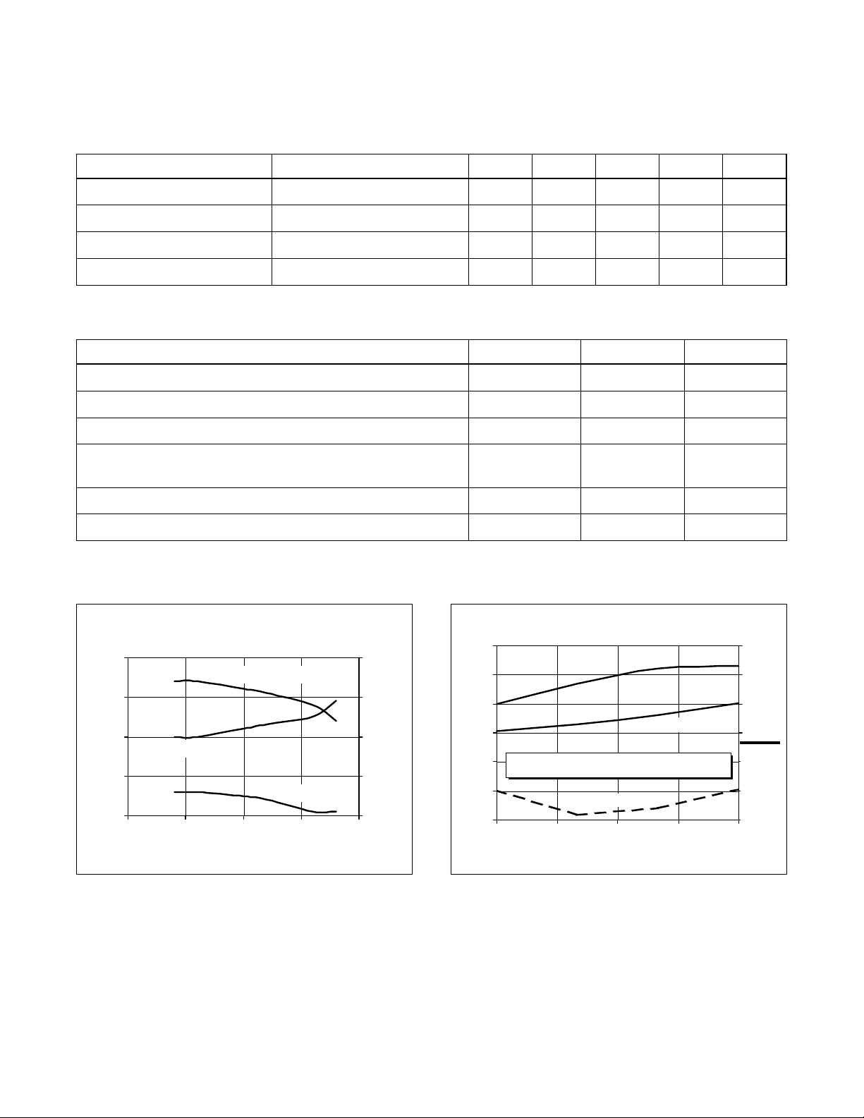
RF Specifications (100% T ested)
Characteristic Symbol Min T yp Max Units
Gain
(V
Power Output at 1 dB Compression
(V
Drain Efficiency
(V
Load Mismatch Tolerance
(V
—all phase angles at frequency of test)
All published data at T
= 28 V , P
DD
= 28 V , IDQ = 600 mA, f = 960 MHz) P-1dB 70 75 — Watts
DD
= 28 V , P
DD
= 28 V , Pout = 70 W , IDQ = 600 mA, f = 960 MHz Y — — 10:1 —
DD
= 70 W, IDQ = 600 mA, f = 960 MHz) G
out
= 70 W, IDQ = 600 mA, f = 960 MHz) h 45 50 — %
out
= 25°C unless otherwise indicated.
CASE
pe
13.0 14.5 — dB
e
1
PTF 10019
y
R
(dB)
y
s
e
Electrical Characteristics (100% T ested)
Characteristic Conditions Symbol Min Typ Ma x Units
Drain-Source Breakdown Voltage VGS = 0 V , ID = 25 mA V
(BR)DSS
Drain-Source Leakage Current VDS = 26 V , VGS = 0 V I
Gate Threshold Voltage VDS = 10 V , ID = 75 mA V
Forward Transconductance VDS = 10 V , ID = 3 A g
DSS
GS(th)
fs
65 — — Volts
— — 1.0 mA
3.0 — 5.0 Volts
— 3.0 — Siemens
Maximum Ratings
Parameter Symbol Value Unit
Drain-Source Voltage V
Gate-Source Voltage V
Operating Junction T emperature T
T otal Device Dissipation P
DSS
GS
J
D
Above 25°C derate by 1.25 W/°C
Storage T emperature Range T
Thermal Resistance (T
= 70°C) R
CASE
STG
qJC
65 Vdc
±20 Vdc
200 °C
215 Watts
–40 to +150 °C
0.8 °C/W
Typical Performance
Typical P
16
15
14
Power G ai n (d B )
13
, Gain, and Efficiency
OUT
vs. Frequency
Outp ut P ower (W)
Power Gain @ P-1dB
12
800 850 900 950 1000
Frequency (MHz)
(at P-1 dB)
Efficiency (%)
90
80
70
60
50
Output Power and Efficienc
16
14
12
10
Gain
8
6
4
900 915 930 945 960
Broadband Test Fixture Performance
Gain (dB)
Efficiency (%)
VDD = 28 V, IDQ = 600 mA, P
eturn Loss
Frequency (MHz)
OUT
= 70 W
70
60
50
40
- 5
30
-15
20
-25
10
Efficienc
Return Los
2
 Loading...