

Ericsson PTF10009 Datasheet
PTF 10009
85 Watts, 1.0 GHz
GOLDMOS
™
Field Effect Transistor
Description
The PTF 10009 is an 85 Watt LDMOS FET intended for large signal
amplifier applications to 1.0 GHz. It operates at 50% efficiency and
13.0 dB of gain. Nitride surface passivation and full gold metallization
are used to ensure excellent device lifetime and reliability.
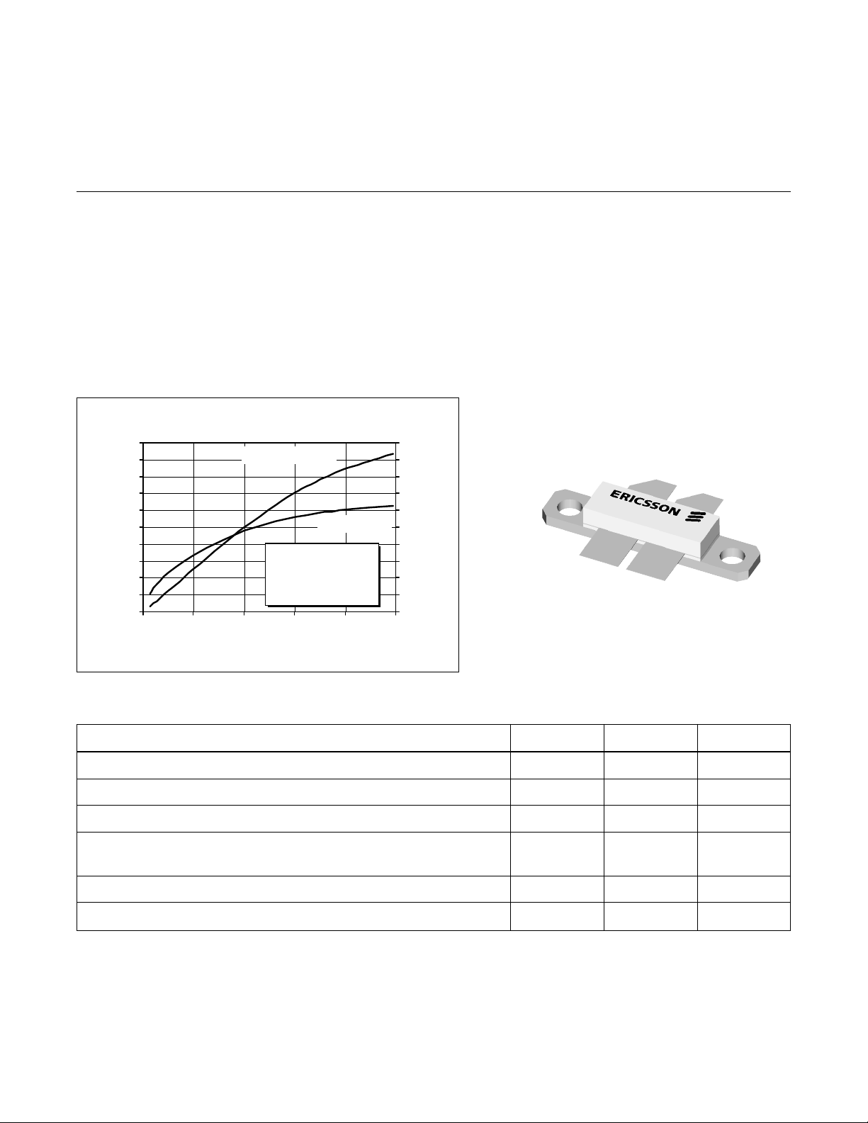
Typical Output Power and Efficiency vs. Input Power
100
90
80
70
60
50
40
30
Output Power
20
10
0
0.0 1.0 2.0 3.0 4.0 5.0
Outpu t Power (W)
VDS = 28 V
I
= 600 mA Total
DQ
f = 960 MHz
Input Power (Watts)
Efficiency (%)
80
72
64
56
48
40
32
24
16
8
0
Efficiency
• Performance at 960 MHz, 28 Volts
- Output Power = 85 Watts
- Power Gain = 13.0 dB Typ
- Efficiency = 50% T yp
• Full Gold Metallization
• Silicon Nitride Passivated
• Excellent Thermal Stability
• 100% lot traceability
10009
1234569744
Package 20230
Maximum Ratings
Parameter Symbol Value Unit
Drain-Source Voltage
Gate-Source Voltage
Operating Junction Temperature T
Total Device Dissipation P
Above 25°C derate by 1.54 W/°C
Storage Temperature Range T
Thermal Resistance (T
(1)
per side
All published data at T
(1)
(1)
= 70°C) R
CASE
= 25°C unless otherwise indicated.
CASE
V
DSS
V
STG
GS
J
D
qJC
65 Vdc
±20 Vdc
200 °C
27 0 Watts
-65 to 150 °C
0.65 °C/W
e
1
PTF 10009
e
Electrical Characteristics (100% Tested—characteristics, conditions and limits shown per side)
Characteristic (per side) Conditions Symbol Min Typ Max Units
Drain-Source Breakdown Voltage VGS = 0 V , ID = 25 mA V
Drain-Source Leakage Current VDS = 28 V , VGS = 0 V I
Gate Threshold Voltage VDS = 10 V , ID = 75 mA V
Forward Transconductance VDS = 10 V , ID = 3 A g
(BR)DSS
DSS
GS(th)
fs
65 — — Volts
— — 1.0 mA
3.0 — 5.0 Volts
— 2.8 — Siemens
Dynamic Characteristics
Characteristic (per side) Symbol Min Typ Max Units
Input Capacitance
(V
Output Capacitance
(V
Reverse Transfer Capacitance
(V
= 28 V, VGS = 0 V, f = 1 MHz) C
DS
= 28 V, VGS = 0 V, f = 1 MHz) C
DS
= 28 V, VGS = 0 V, f = 1 MHz) C
DS
iss
oss
rss
—90—pF
—36—pF
— 1.9 — pF
RF Specifications (100% Tested)
Characteristic Symbol Min Typ Max Units
Gain
(V
Drain Efficiency
(V
Load Mismatch Tolerance
(V
all phase angles at frequency of test)
= 28 V, P
DD
= 28 V, P
DD
= 28 V, P
DD
= 85 W, IDQ = 600 mA, f = 960 MHz) G
out
= 85 W, IDQ = 600 mA, f = 960 MHz) h 47 50 — %
out
= 85 W, IDQ = 600 mA, f = 960 MHz— Y — — 5:1 —
out
ps
12.0 13.0 — dB
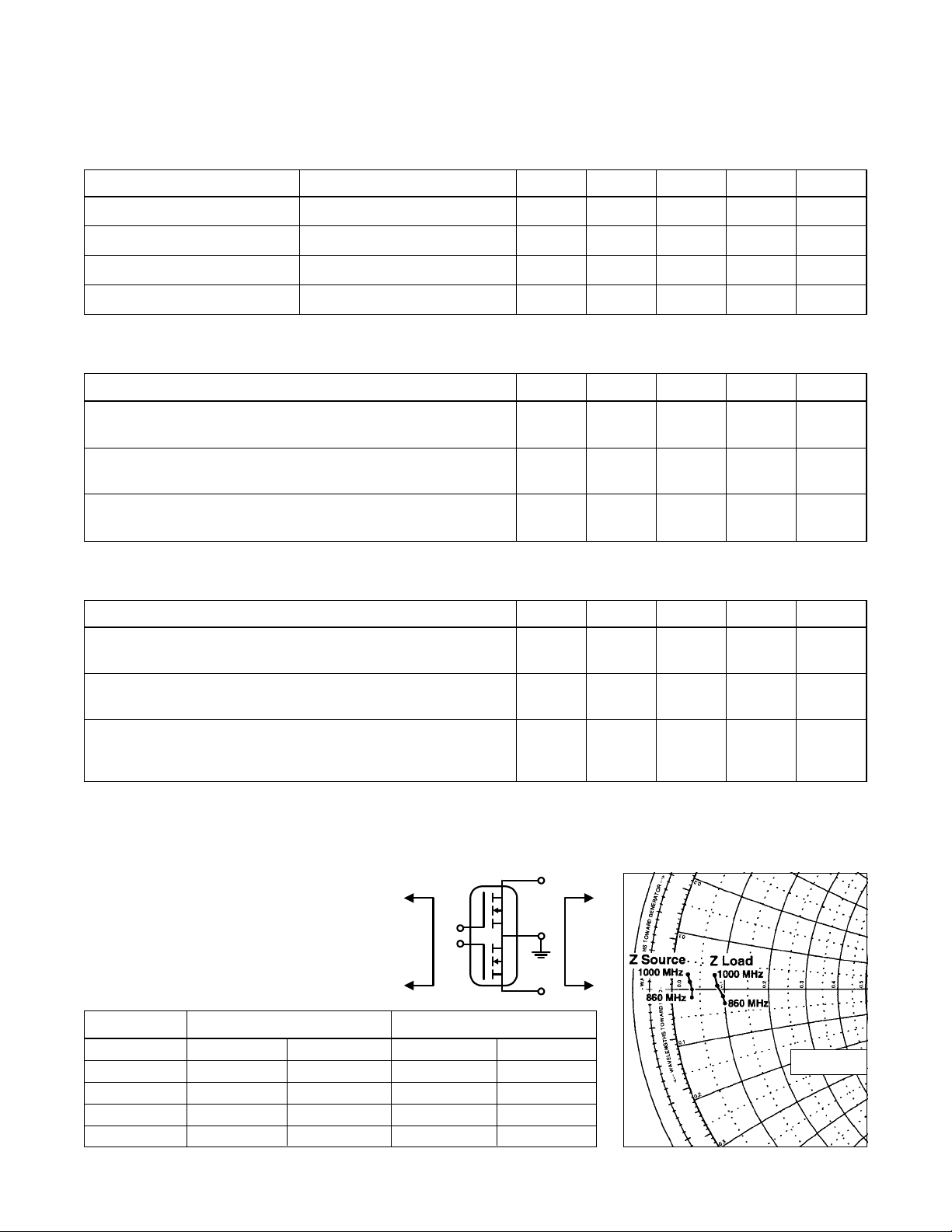
Impedance Data (data shown for fixed-tuned broadband circuit)
(VDD = 28 V, P
Frequency Z Source W Z Load W
MHz R jX R jX
860 1.76 -0.78 5.00 -1.50
900 1.80 -0.05 4.80 -0.78
960 1.58 0.69 4.24 0.36
1000 1.39 1.35 3.95 1.41
= 85 W, IDQ = 600 mA)
out
Z Source Z Load
G
G
2
D
S
D
Z0 = 50 W
 Loading...