

Ericsson PTB20258 Datasheet
e
r
Cellular Radio RF Power Transistor
Description
Description
The 20258 is a class AB, NPN, common emitter RF power transistor
The 20258 is a class AB, NPN, common emitter RF power transistor
intended for 25 Vdc operation from 915 to 960 MHz. Rated at 6 watts
intended for 25 Vdc operation from 915 to 960 MHz. Rated at 6 watts
minimum output power, it may be used for both CW and PEP
minimum output power, it may be used for both CW and PEP
applications. Ion implantation, nitride surface passivation and gold
applications. Ion implantation, nitride surface passivation and gold
metallization are used to ensure excellent device reliability . 100% lot
metallization are used to ensure excellent device reliability . 100% lot
traceability is standard.
traceability is standard.
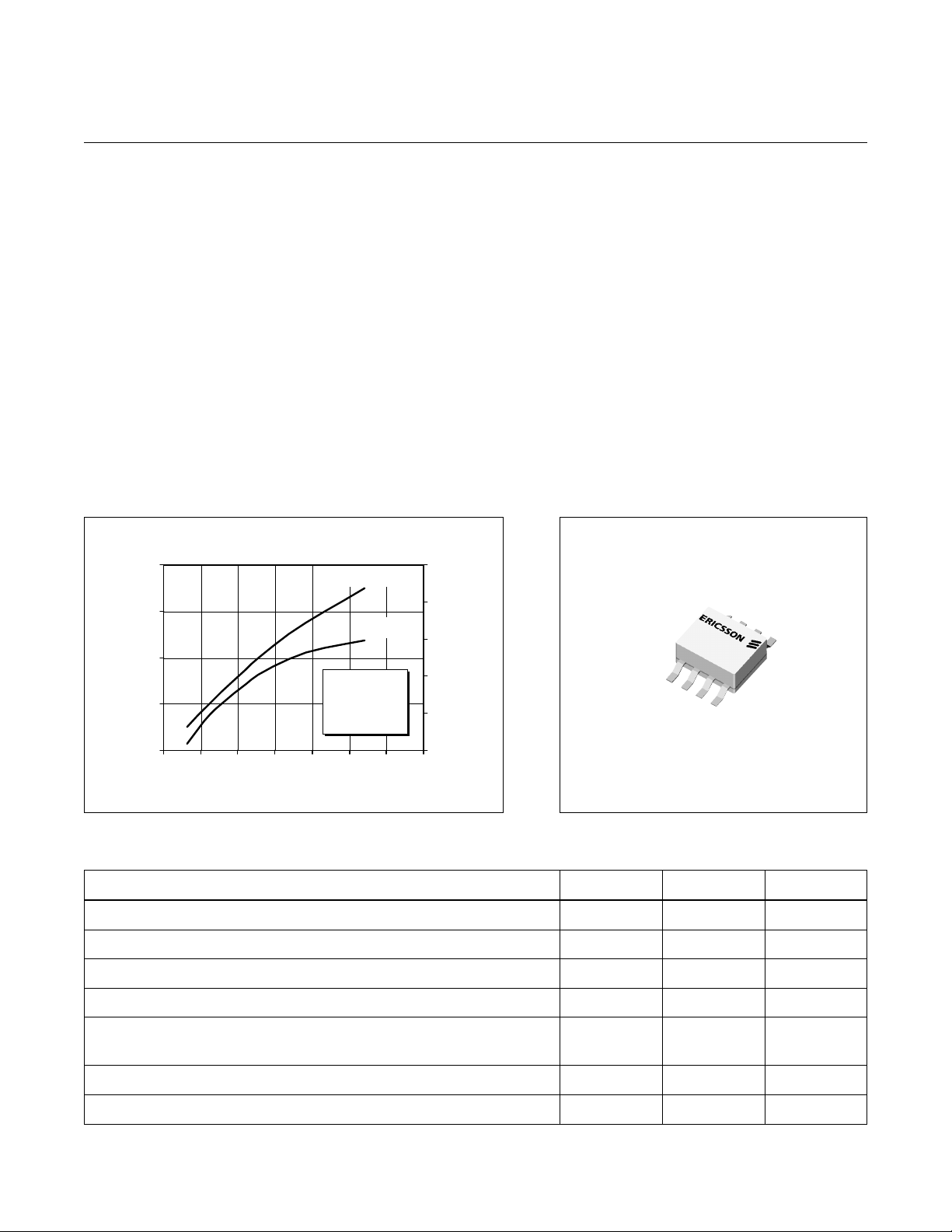
Typical Output Pow er and Efficiency vs. Input Power
8
6
4
2
Output Power (Watts)
0
0.0 0.1 0.2 0.3 0.4 0.5 0.6 0.7
Input Power (Watts)
Output Powe
Efficiency
VCC = 25 V
I
= 27 mA
CQ
f = 960 MHz
80
68
56
44
Efficiency (%)
32
20
PTB 20258
6 Watts, 915–960 MHz
6 Watts, 915–960 MHz
Class AB Characteristics
50% Typ Collector Efficiency at 6 Watts
Tested to solderability standards:
- IEC-68-2-54
- ANSI/J Std-002-A
Gold Metallization
Silicon Nitride Passivated
20258
LOT CODE
Package 20208
Maximum Ratings
Parameter Symbol Value Unit
Collector-Emitter Voltage V
Collector-Base Voltage V
Emitter-Base Voltage (collector open) V
Collector Current (continuous) I
Total Device Dissipation at T
Above 25°C derate by 0.125 W/°C
Storage Temperature Range T
Thermal Resistance (T
7-21-98
flange
= 25°C P
flange
= 70°C) R
1
CER
CBO
EBO
C
D
stg
θJC
55 Vdc
60 Vdc
4.0 Vdc
1.7 Adc
22 Watts
-40 to +150 °C
8 °C/W
PTB 20258
e
Electrical Characteristics (100% Tested)
Characteristic Conditions Symbol Min Typ Max Units
Breakdown Voltage C to E IB = 0 A, IC = 50 mA V
Breakdown Voltage C to E VBE = 0 V, IC = 50 mA V
Breakdown Voltage E to B IC = 0 A, IE = 5 mA V
DC Current Gain VCE = 5 V, IC = 1 A h
(BR)CEO
(BR)CES
(BR)EBO
FE
28 29 — Volts
60 70 — Volts
3.5 5 — Volts
20 50 120 —
RF Specifications (100% Tested)
Characteristic Symbol Min Typ Max Units
Gain
(V
Collector Efficiency
(V
Load Mismatch Tolerance
(V
f = 960 MHz—all phase angles at frequency of test)
= 25 Vdc, P
CC
= 25 Vdc, P
CC
= 25 Vdc, P
CC
= 6 W, ICQ = 27 mA, f = 960 MHz) G
out
= 6 W, ICQ = 27 mA, f = 960 MHz) η
out
= 6 W, ICQ = 27 mA, Ψ — — 30:1 —
out
pe
C
10 11 — dB
—50—%
Typical Performance
Gain vs. Frequency
(as measured in a broadband circuit)
13
VCC = 25 V
12
I
= 27 mA
CQ
P
= 6 W
OUT
11
Gain (dB)
10
9
700 750 800 850 900 950 1000 1050
Frequency (MHz)
Output Power
9
8
7
6
5
4
Output Power (Watts)
3
ICQ = 27 mA
f = 960 MHz
20 22 24 26 28
(at P-1dB)
Supply Voltage (Volts)
vs. Supply Voltage
7-21-98
2
 Loading...