

Ericsson PTB20245 Datasheet
e
Wide-Band CDMA Power Transistor
Description
The 20245 is a class AB, NPN common emitter RF power transistor
intended for 26 Vdc operation from 2.1 to 2.2 GHz frequency band.
Rated at 35 watts minimum output power for PEP applications, it is
specifically intended for operation as a final or driver stage in Wide
CDMA or TDMA systems. Ion implantation, nitride surface passivation
and gold metallization ensure excellent device reliability. 100% lot
traceability is standard.
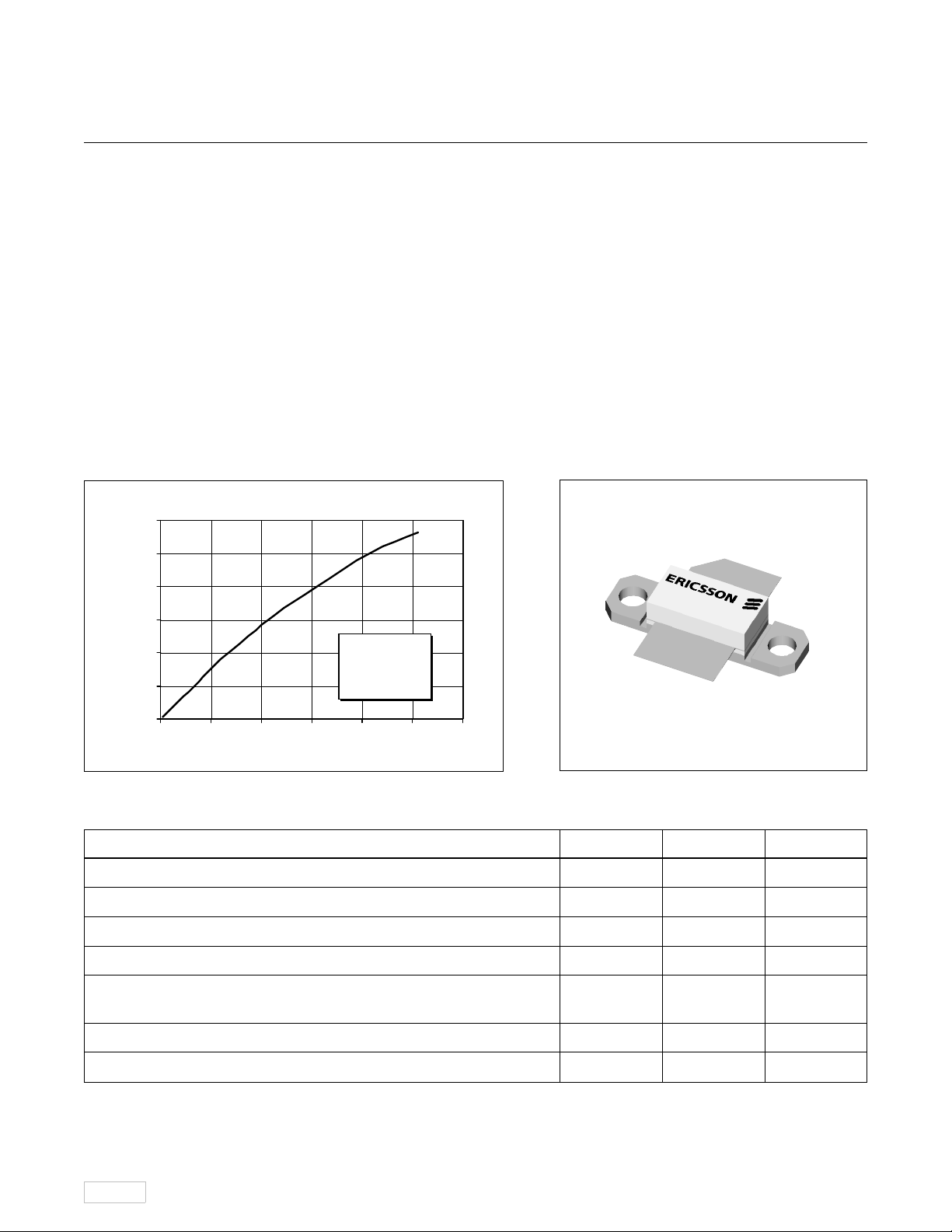
Typical Output Pow er vs. Input Pow er
60
50
PTB 20245
35 Watts, 2.1–2.2 GHz
• 35 Watts, 2.1–2.2 GHz
• Class AB Characteristics
• Gold Metallization
• Silicon Nitride Passivated
40
30
20
10
Output Power (Watts)
0
024681012
Input Power (Wa tts)
VCC = 26 V
I
= 100 mA
CQ
f = 2000 MHz
20245
LOT CODE
Package 20223
Maximum Ratings
Parameter Symbol Value Unit
Collector-Emitter Voltage V
Collector-Base Voltage V
Emitter-Base Voltage (collector open) V
Collector Current (continuous) I
Total Device Dissipation at T
Above 25°C derate by 1.2 W/°C
Storage Temperature Range T
Thermal Resistance (T
flange
= 25° C P
flange
= 70° C) R
CER
CBO
EBO
C
D
STG
θJC
55 Vdc
55 Vdc
3.5 Vdc
7.7 Adc
200 Watts
–40 to +150 °C
0.85 °C/W
9/28/98
1
PTB 20245
y
)
)
e
Electrical Characteristics (100% Tested)
Characteristic Conditions Symbol Min Ty p Max Units
Breakdown Voltage C to E VBE = 0 V, IC = 20 mA V(
Breakdown Voltage C to E IB = 0 A, IC = 20 mA, RBE = 22 Ω V(
Breakdown Voltage E to B IC = 0 A, IE = 5 mA V(
BR)CES
BR)CER
BR)EBO
DC Current Gain VCE = 10 V, IC = 1.5 A h
FE
55 — — Volts
55 — — Volts
3.5 4.0 — Volts
30 40 — —
RF Specifications (100% Tested)
Characteristic Symbol Min Typ Max Units
Gain
(V
= 26 Vdc, P
CC
Power Output at 1 dB Compression
(V
= 26 Vdc, ICQ = 85 mA, f = 2.2 GHz) P–1dB 35.0 — — Watts
CC
Collector Efficiency
(V
= 26 Vdc, P
CC
Load Mismatch Tolerance
(V
= 26 Vdc, P
CC
f = 2.2 GHz—all phase angles at frequency of test)
= 10 W, ICQ = 85 mA, f = 2.2 GHz) G
out
= 35 W, ICQ = 85 mA, f = 2.2 GHz) η
out
= 17.5 W, ICQ = 85 mA Ψ — — 5:1 —
out
pe
C
7.5 8.5 — dB
—40—%
Typical Performance
Typical P
12
11
10
, Gain & Efficiency
OUT
vs. Frequenc
Outp ut P ower (W)
VCC = 26 V
9
Gain (dB)
8
Gain (dB)
7
2050 2100 2150 2200 2250
I
= 250 mA
CQ
Frequency (MHz)
(at P-1dB)
Efficiency (%)
Broadband Test Fixture Performance
60
55
50
45
40
35
30
25
Output Power & Efficiency
20
10
8
6
Gain (dB)
4
2
2100 2120 2140 2160 2180 2200
Gain (dB)
VCC = 26 V
I
= 85 mA
CQ
Pout = 35 W
Return Loss (dB)
Frequency (MHz)
Efficiency (%)
60
50
40
Efficiency (%
- 5
30
-15
20
-25
10
-35
0
Return Loss (dB
2
4/3/98
 Loading...