

Ericsson PTB20200, PTB20204 Datasheet

e
1
0.0
0.4
0.8
1.2
1.6
2.0
0.00 0.03 0.06 0.09 0.12 0.15
Input Power (Watts)
Output Power (Watts)
VCE = 24 V
I
CQ
= 340 mA
f = 500 MHz
Typical Output Pow er vs. Input Pow er
PTB 20204
1.0 Watt, 380–500 MHz
RF Power Transistor
Package 20227
20204
LOT CODE
Description
The 20204 is a class A, NPN, common emitter RF power transistor
intended for 24 Vdc operation from 380 to 500 MHz. Rated at 1.0
watt minimum output power, it may be used for both CW and PEP
applications. Ion implantation, nitride surface passivation and gold
metallization ensure excellent device reliability. 100% lot traceability
is standard.
1.0 Watt, 380–500 MHz
Class A Characteristics
-40 dB Max Two-Tone IMD at 1.0 W(PEP)
Gold Metallization
Silicon Nitride Passivated
Maximum Ratings
Parameter Symbol Value Unit
Collector-Emitter Voltage V
CER
60 Vdc
Collector-Base Voltage V
CBO
60 Vdc
Emitter-Base Voltage (collector open) V
EBO
4.0 Vdc
Collector Current (continuous) I
C
0.5 Adc
Total Device Dissipation at T
flange
= 25°C P
D
11 Watts
Above 25°C derate by 0.0625 W/°C
Storage Temperature Range T
STG
-40 to +150 °C
Thermal Resistance (T
flange
= 70°C) R
θJC
16 °C/W
9/28/98
PTB 20204
2
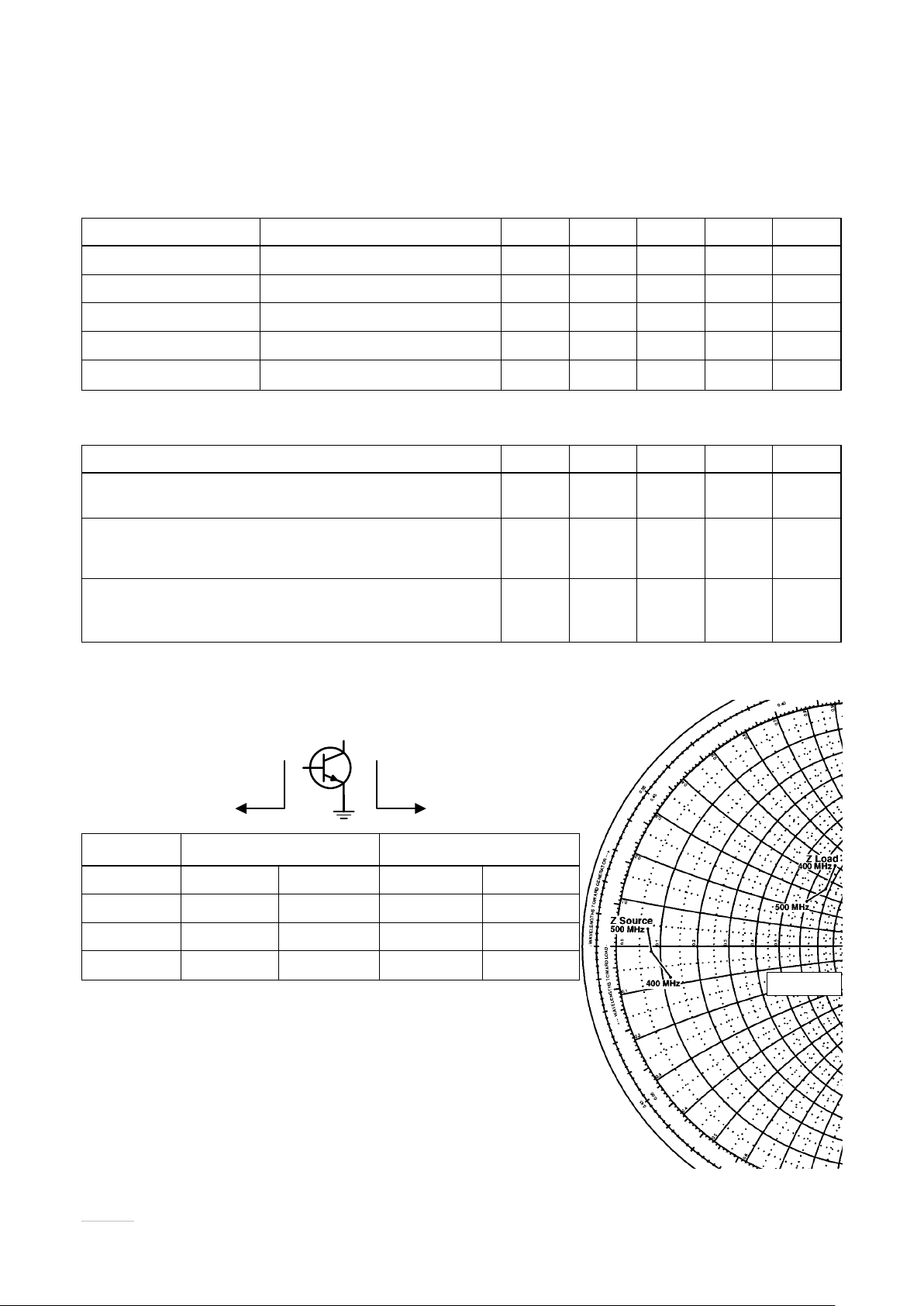
e
Z Source Z Load
Electrical Characteristics (100% Tested)
Characteristic Conditions Symbol Min Typ Max Units
Breakdown Voltage C to E IB = 0 A, IC = 5 mA V
(BR)CEO
25 30 — Volts
Breakdown Voltage C to E VBE = 0 V, IC = 5 mA V
(BR)CES
70 — — Volts
Breakdown Voltage E to B IC = 0 A, IE = 5 mA V
(BR)EBO
4 5 — Volts
DC Current Gain VCE = 5 V, IC = 250 mA h
FE
20 40 — —
Output Capacitance VCB = 24 V, IE = 0 A, f = 1 MHz C
obo
— 4.4 — pF
RF Specifications (100% Tested)
Characteristic Symbol Min Typ Max Units
Gain
(V
CE
= 24 Vdc, P
out
= 1.0 W, ICQ = 340 mA, f = 500 MHz) G
pe
12.5 13.5 — dB
Two-Tone Intermodulation Distortion
(V
CE
= 24 Vdc, P
out
= 1.0 W(PEP), ICQ = 340 mA, IM
2
— -44 -40 dB
f1 = 500 MHz, f2 = 501 MHz)
Load Mismatch Tolerance
(V
CE
= 24 Vdc, P
out
= 2 W, ICQ = 340 mA, Ψ — — 30:1 —
f = 500 MHz—all phase angles at frequency of test)
Impedance Data (data shown for fixed-tuned broadband circuit)
(V
CE
= 24 Vdc, Pout = 1.0 W, ICQ = 340 mA)
Frequency Z Source Z Load
MHz R jX R jX
400 6.0 -4.0 33.2 24.9
450 3.9 -0.6 34.0 17.3
500 3.4 2.1 30.1 12.2
Z0 = 50 Ω
5/14/98
 Loading...