

Ericsson PTB20190 Datasheet
e
Description
PTB 20190
175 Watts, 470–806 MHz
Digital Television Power Transistor
The 20190 is a class AB, NPN, common emitter RF power transistor
intended for 28 Vdc operation across the 470 to 806 MHz UHF TV
frequency band. Rated at 175 watts output power, it is specifically
intended to operate uncorrected at 125 watts P-Sync (tested to EIA
Standard 4.1.3, Section 5, Method B for class AB transmitters at 125
watts P-sync) or at a minimum of 175 watts in PEP applications. It
may also be operated at comparable power levels for ATV broadcasting. Ion implantation, nitride surface passivation and gold metallization ensure excellent device reliability. 100% lot traceability is
standard.
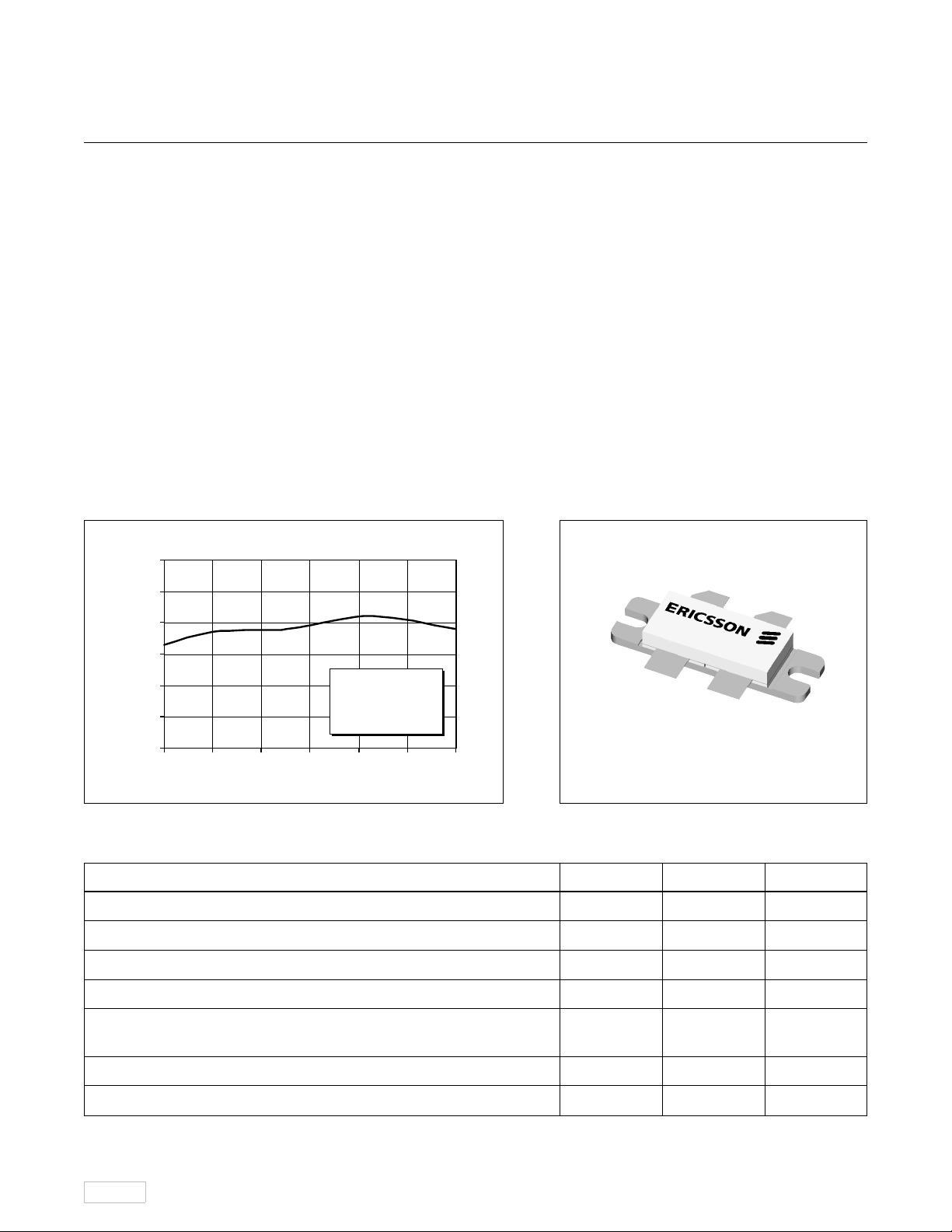
Typical Gain vs. Frequency
10.5
10.0
9.5
9.0
8.5
Gain (dB)
8.0
7.5
470 526 582 638 694 750 806
Frequency (MHz)
VCC = 28 V
I
= 2 x 100 mA
CQ
Pout = 175 W
175 Watts, 470–806 MHz
Class AB Characteristics
50% Collector Efficiency at 175 Watts
Gold Metallization
Silicon Nitride Passivated
20190
LOT CODE
Package 20224
Maximum Ratings
Parameter Symbol Value Unit
Collector-Emitter Voltage V
Collector-Base Voltage V
Emitter-Base Voltage (collector open) V
Collector Current (continuous) I
Total Device Dissipation at T
Above 25°C derate by 1.89 W/°C
Storage Temperature Range T
Thermal Resistance (T
9/28/98
flange
= 25°C P
flange
= 70°C) R
1
CER
CBO
EBO
C
D
STG
θJC
40 Vdc
60 Vdc
4.0 Vdc
25.0 Adc
330 Watts
–40 to +150 °C
0.53 °C/W
PTB 20190
5
e
Electrical Characteristics (100% Tested)
Characteristic Conditions Symbol Min Typ Max Units
Breakdown Voltage C to E IB = 0 A, IC = 100 mA V
Breakdown Voltage C to E VBE = 0 V, IC = 100 mA V
Breakdown Voltage E to B IC = 0 A, IE = 5 mA V
DC Current Gain VCE = 5 V, IC = 1.0 A h
(BR)CEO
(BR)CES
(BR)EBO
FE
25 30 — Volts
55 60 — Volts
3.5 5 — Volts
20 50 100 —
RF Specifications (100% Tested)
Characteristic Symbol Min Typ Max Units
Gain
(V
Collector Efficiency
(V
Intermodulation Distortion (Two Tone)
(V
f = 800 MHz, ∆f = 1.0 MHz)
In-Channel Intermodulation Distortion
(P-Sync = 125 W + Aural,
EIA Std 4.1.3 Sect 5 Method B)
Load Mismatch Tolerance
(V
f = 800 MHz—all phase angles at frequency of test)
= 28 Vdc, P
CC
= 28 Vdc, P
CC
= 28 Vdc, P
CC
= 28 Vdc, P
CC
= 50 W, ICQ = 2 x 100 mA, f = 800 MHz) G
OUT
= 125 W, ICQ = 2 x 100 mA, f = 800 MHz) η
OUT
= 125 W(PEP), ICQ = 2 x 100 mA, IMD — 40 — dBc
OUT
= 125 W(PEP), ICQ = 2 x 100 mA, Ψ — — 3:1 —
OUT
pe
C
IM Product
+/- 920 kHz
8.0 9.5 — dB
—45—%
— -52 — dB
P-sync
Impedance Data
V
= 28 Vdc, P
CC
Frequency Z Source Z Load
MHz R jX R jX
470 1.87 -4.1 2.42 1.74
630 0.76 -3.9 3.34 -1.49
800 2.12 -3.8 2.72 -3.36
= 175 W, ICQ = 2 x 100 mA
OUT
Z Source Z Load
2
Z0 = 50 Ω
/11/98
 Loading...