

Ericsson PTB20167 Datasheet
e
Description
PTB 20167
60 Watts, 850–960 MHz
RF Power Transistor
The 20167 is an NPN, common base RF power transistor intended
for 24 Vdc operation from 850 to 960 MHz. Rated at 60 watts minimum
output power, it is specifically designed for class C power amplifier
applications. Ion implantation, nitride surface passivation and gold
metallization are used to ensure excellent device reliability . 100% lot
traceability is standard.
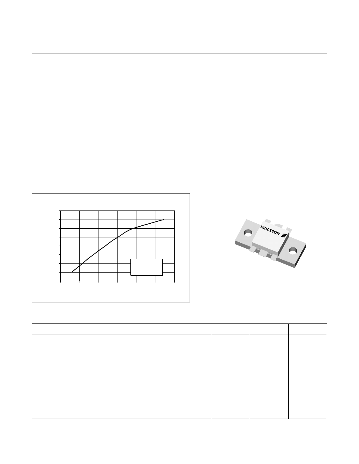
Typical Output Pow er vs. Input Pow er
70
65
60
55
50
45
40
Output Power (Watts)
35
30
6789101112
Input Power (Watts)
VCC = 24 V
f = 905 MHz
24 Volt, 905 MHz Common Base Characteristics
- Output Power = 60 W
- Power Gain = 7.0 dB Min
- Efficiency = 60% Min
Double Input/Output Matched for Wideband
Performance
Gold Metallization
Silicon Nitride Passivated
20167
LOT CODE
Package 20200
Maximum Ratings
Parameter Symbol Value Unit
Collector-Emitter Voltage V
Collector-Base Voltage V
Emitter-Base Voltage (collector open) V
Collector Current (continuous) I
Total Device Dissipation at T
Above 25°C derate by 1 W/°C
Storage Temperature Range T
Thermal Resistance (T
9/28/98
flange
= 25°C P
flange
= 70°C) R
1
CEO
CBO
EBO
C
D
STG
θJC
30 Vdc
55 Vdc
4.0 Vdc
10 Adc
175 Watts
–40 to +150 °C
1 °C/W

PTB 20167
e
Electrical Characteristics (100% Tested)
Characteristic Conditions Symbol Min Typ Max Units
Breakdown Voltage C to E IB = 0 A, IC = 50 mA V
Breakdown Voltage C to E VBE = 0 V, IC = 50 mA V
Breakdown Voltage E to B IC = 0 A, IE = 15 mA V
DC Current Gain VCE = 5 V, IC = 2.0 A h
Output Capacitance VCB = 28 V, f = 1 MHz C
(BR)CEO
(BR)CES
(BR)EBO
FE
ob
30 — — Volts
55 — — Volts
4.0 — — Volts
20 — 100 —
—60—pF
RF Specifications (100% Tested)
Characteristic Symbol Min Typ Max Units
Common Base Power Gain
(V
Collector Efficiency
(V
Load Mismatch Tolerance
(V
f = 905 MHz—all phase angles at frequency of test)
= 24 Vdc, P
CC
= 24 Vdc, P
CC
= 24 Vdc, P
CC
= 60 W, f = 905 MHz) G
out
= 60 W, f = 905 MHz) η
out
= 60 W, Ψ — — 5:1 —
out
pb
C
7.0 7.9 — dB
60 64 — %
Impedance Data (data shown for fixed-tuned broadband circuit)
(V
= 24 Vdc, P
CC
= 60 W)
out
Z Source Z Load
Frequency Z Source Z Load
MHz R jX R jX
850 5.4 -3.6 5.8 -0.7
905 5.3 -2.4 6.2 0.6
960 5.2 -1.4 6.9 1.7
2
 Loading...