

Ericsson PTB20146 Datasheet
e
Description
PTB 20146
0.4 Watt, 1.8–2.0 GHz
Cellular Radio RF Power Transistor
The 20146 is a class A, NPN, common emitter RF power transistor
intended for 26 Vdc operation from 1.8 to 2.0 GHz. Rated at 0.4 watt
minimum output power, it may be used for both CW and PEP
applications. Ion implantation, nitride surface passivation and gold
metallization are used to ensure excellent device reliability . 100% lot
traceability is standard.
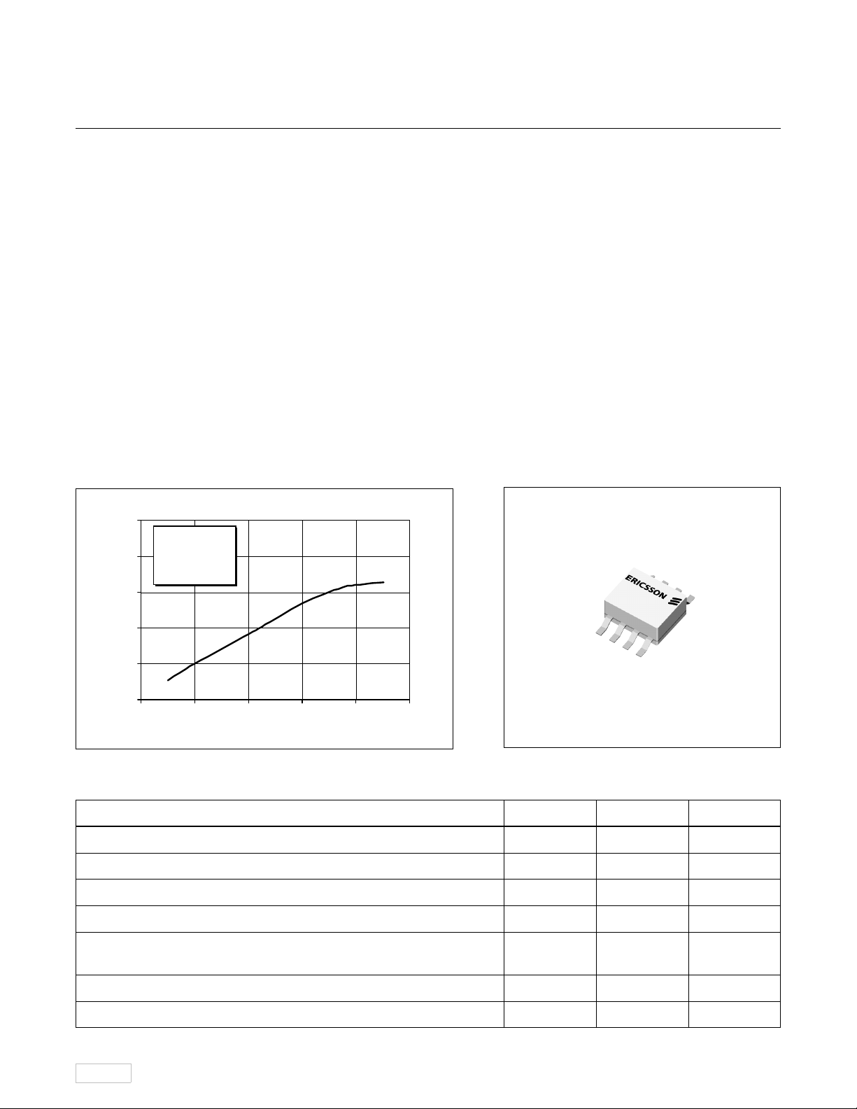
Typical Output Pow er vs. Input Power
1.0
VCC = 26 V
0.8
I
= 140 mA
CQ
f = 2.0 GHz
0.6
0.4
0.2
Output Power (Watts)
0.0
0.00 0.02 0.04 0.06 0.08 0.10
Input Power (Wa tts)
0.4 Watt, 1.8–2.0 GHz
Class A Characteristics
Tested to solderability standards:
- IEC-68-2-54
- ANSI/J Std-002-A
Gold Metallization
Silicon Nitride Passivated
Surface Mountable
Available in Tape and Reel
20146
LOT CODE
Package 20208
Maximum Ratings
Parameter Symbol Value Unit
Collector-Emitter Voltage V
Collector-Base Voltage V
Emitter-Base Voltage (collector open) V
Collector Current (continuous) I
Total Device Dissipation at T
Above 25°C derate by 0.031 W/°C
Storage Temperature Range T
Thermal Resistance (T
9/28/98
flange
= 25°C P
flange
= 70°C) R
1
CER
CBO
EBO
C
D
STG
θJC
50 Vdc
50 Vdc
4.0 Vdc
0.5 Adc
5.4 Watts
–40 to +150 °C
32.3 °C/W
PTB 20146
5
e
Electrical Characteristics (100% Tested)
Characteristic Conditions Symbol Min Typ Max Units
Breakdown Voltage C to E IB = 0 A, IC = 10 mA, RBE = 22 Ω V
Breakdown Voltage C to E VBE = 0 V, IC = 5 mA V
Breakdown Voltage E to B IC = 0 A, IE = 5 mA V
DC Current Gain VCE = 5 V, IC = 250 mA h
(BR)CER
(BR)CES
(BR)EBO
FE
50 — — Volts
50 — — Volts
4 5 — Volts
20 40 — —
RF Specifications (100% Tested)
Characteristic Symbol Min Typ Max Units
Gain
(V
Output Power at 1 dB Compressed
(V
Load Mismatch Tolerance
(V
f = 2.0 GHz—all phase angles at frequency of test)
= 26 Vdc, P
CC
= 26 Vdc, ICQ = 140 mA, f = 2.0 GHz) P-1dB 0.4 0.6 — Watts
CC
= 26 Vdc, P
CC
= 0.4 W, ICQ = 140 mA, f = 2.0 GHz) G
out
= 0.4 W, ICQ = 140 mA, Ψ — — 5:1 —
out
pe
810—dB
Impedance Data (data shown for fixed-tuned broadband circuit)
(V
= 26 Vdc, P
CC
= 0.4 W, ICQ = 140 mA)
out
Frequency Z Source Z Load
Ericsson Components
RF Power Products
675 Jarvis Drive
Morgan Hill, CA 95037 USA
Telephone: 408-778-9434
Z Source Z Load
GHz R jX R jX
1.800 18.8 3.0 5.8 22.0
1.900 18.1 5.3 8.6 22.4
2.000 18.1 9.3 5.0 21.6
1-877-GOLDMOS
(1-877-465-3667)
e-mail: rfpower@ericsson.com
www.ericsson.com/rfpower
2
Specifications subject to change without notice.
LF
© Ericsson Components AB 1995
EUS/KR 1301-PTB 20146 Uen Rev. D 09-28-98
/19/98
 Loading...