

Ericsson PTB20144 Datasheet
e
Description
PTB 20144
6 Watts, 915–960 MHz
Cellular Radio RF Power Transistor
The 20144 is a class AB, NPN, common emitter RF power transistor
intended for 25 Vdc operation from 915 to 960 MHz. Rated at 6 watts
minimum output power, it may be used for both CW and PEP
applications. Ion implantation, nitride surface passivation and gold
metallization are used to ensure excellent device reliability . 100% lot
traceability is standard.
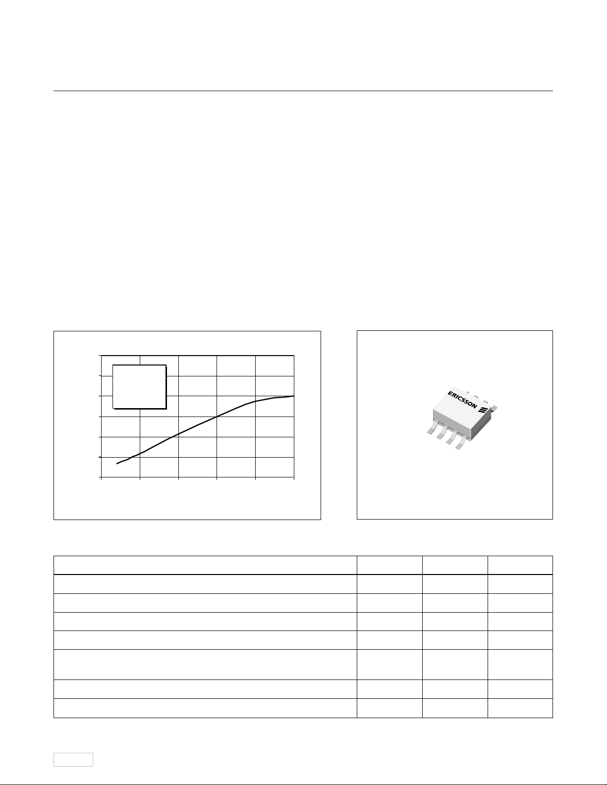
Typical Output Pow er vs. Input Pow er
12
VCC = 25 V
10
= 50 mA
I
CQ
8
f = 960 MHz
6
4
2
Output Power (Watts)
0
0.00 0.25 0.50 0.75 1.00 1.25
Input Power (Wa tts)
6 Watts, 915–960 MHz
Class AB Characteristics
50% Typ Collector Efficiency at 6 Watts
Tested to solderability standards:
- IEC-68-2-54
- ANSI/J Std-002-A
Gold Metallization
Silicon Nitride Passivated
20144
LOT CODE
Package 20208
Maximum Ratings
Parameter Symbol Value Unit
Collector-Emitter Voltage V
Collector-Base Voltage V
Emitter-Base Voltage (collector open) V
Collector Current (continuous) I
Total Device Dissipation at T
Above 25°C derate by 0.125 W/°C
Storage Temperature Range T
Thermal Resistance (T
9/28/98
flange
= 25°C P
flange
= 70°C) R
1
CER
CBO
EBO
C
D
stg
θJC
55 Vdc
60 Vdc
4.0 Vdc
1.7 Adc
22 Watts
–40 to +150 °C
8 °C/W
PTB 20144
e
Electrical Characteristics (100% Tested)
Characteristic Conditions Symbol Min Typ Max Units
Breakdown Voltage C to E IB = 0 A, IC = 50 mA V
Breakdown Voltage C to E VBE = 0 V, IC = 50 mA V
Breakdown Voltage E to B IC = 0 A, IE = 5 mA V
DC Current Gain VCE = 5 V, IC = 1 A h
(BR)CEO
(BR)CES
(BR)EBO
FE
24 30 — Volts
60 70 — Volts
3.5 5 — Volts
20 50 120 —
RF Specifications (100% Tested)
Characteristic Symbol Min Typ Max Units
Gain
(V
Collector Efficiency
(V
Load Mismatch Tolerance
(V
f = 960 MHz—all phase angles at frequency of test)
= 25 Vdc, P
CC
= 25 Vdc, P
CC
= 25 Vdc, P
CC
= 6 W, ICQ = 50 mA, f = 960 MHz) G
out
= 6 W, ICQ = 50 mA, f = 960 MHz) η
out
= 6 W, ICQ = 50 mA, Ψ — — 30:1 —
out
pe
C
910—dB
—50—%
Impedance Data (data shown for fixed-tuned broadband circuit)
(V
= 25 Vdc, P
CC
= 6 W, ICQ = 50 mA)
out
Z Source Z Load
Frequency Z Source Z Load
MHz R jX R jX
915 2.5 -1.4 6.3 9.8
960 2.6 -0.8 7.0 12.4
2
 Loading...