

Ericsson PTB20080 Datasheet
e
Description
PTB 20080
25 Watts, 1.6–1.7 GHz
RF Power Transistor
ThPTB 20080 is a class A/AB, NPN, silicon bipolar junction, internallymatched RF power transistor intended for 26 Vdc operation from 1.6
to 1.7 GHz. It is rated at 25 Watts minimum output power for PEP
applications. Ion implantation, nitride surface passivation and gold
metallization ensure excellent device reliability. 100% lot traceability
is standard.
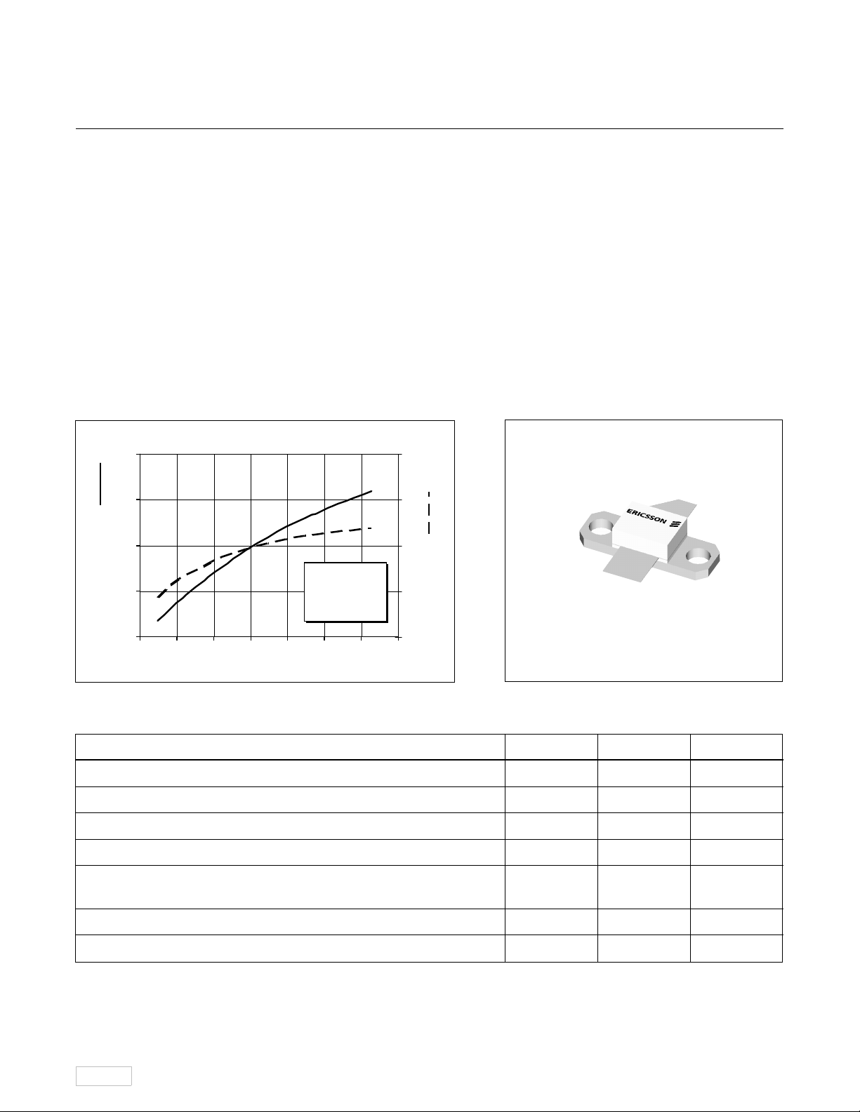
Typical Output Pow er & Efficiency vs. Input Power
40
30
20
VCC = 26 V
10
Output Power (Watts)
0
0.0 0.5 1.0 1.5 2.0 2.5 3.0 3.5
Input Power (Wa tts)
I
= 125 mA
CQ
f = 1.65 GHz
80
60
40
20
Efficiency (%)
0
Maximum Ratings
25 Watts, 1.6–1.7 GHz
Class AB Characteristics
40% Collector Efficiency at 25 Watts
Gold Metallization
Silicon Nitride Passivated
20080
EXXX
Package 20209
Parameter Symbol Value Unit
Collector-Emitter Voltage V
Collector-Base Voltage V
Emitter-Base Voltage (collector open) V
Collector Current (continuous) I
Total Device Dissipation at T
Above 25° C derate by 0.7 W/°C
Storage Temperature Range T
Thermal Resistance (T
9/28/98
flange
= 25° C P
flange
= 70°C) R
1
CER
CBO
EBO
C
D
STG
θJC
50 Vdc
50 Vdc
4.0 Vdc
3.4 Adc
123 Watts
150 °C
1.43 °C/W
PTB 20080
5
e
Electrical Characteristics (100% Tested)
Characteristic Conditions Symbol Min Typ Max Units
Breakdown Voltage C to B VBE = 0 V, IC = 15 mA V
Breakdown Voltage E to B IC = 5 mA V
Cut-off Current C to E VCE = 26 V I
DC Current Gain VCE = 5 V, IC = 2 A h
(BR)CES
(BR)EBO
CES
FE
50 — — Vdc
4.0 — — Vdc
——10mA
30 — — —
RF Specifications (100% Tested)
Characteristic Symbol Min Typ Max Units
Power Gain
(V
= 26 Vdc, P
CC
Power Output at 1 dB Compression
(V
Collector Efficiency
(V
Load Mismatch Tolerance
(V
f = 1.65 GHz—all phase angles at frequency of test)
= 26 Vdc, ICQ = 125 mA, f = 1.65 GHz) P-1dB 25 — — Watts
CC
= 26 Vdc, P
CC
= 26 Vdc, P
CC
= 10 W, ICQ = 125 mA, f = 1.65 GHz) G
OUT
= 25 W, ICQ = 125 mA, f = 1.65 GHz) η
OUT
= 25 W, ICQ = 125 mA, Ψ — — 10:1 —
OUT
pe
C
10.5 11.5 — dB
40 44 — %
Impedance Data (data shown for fixed-tuned broadband circuit)
V
= 26 Vdc, P
CC
= 25 W, ICQ = 125 mA
OUT
Z Source Z Load
Frequency Z Source Z Load
GHz R jX R jX
1.60 5.6 -4.1 2.6 -1.0
1.65 5.6 -4.0 2.6 -0.6
1.70 5.6 -4.0 2.7 -0.2
Z0 = 50 Ω
2
/6/98
 Loading...