

Page 1
PKJ 4000 PI
37.5-150W DC/DC Power Modules
48V Input Series
• High efficiency 91.5% Typ (5V)
at full load
• Industry standard footprint
• Max case temperature +100ºC
• Wide input voltage range according
to ETSI specifications
• High power density, up to 55W/in
3
• 1,500 Vdc isolation voltage
• MTBF > 3 million hours in
accordance with Bellcore TR-332
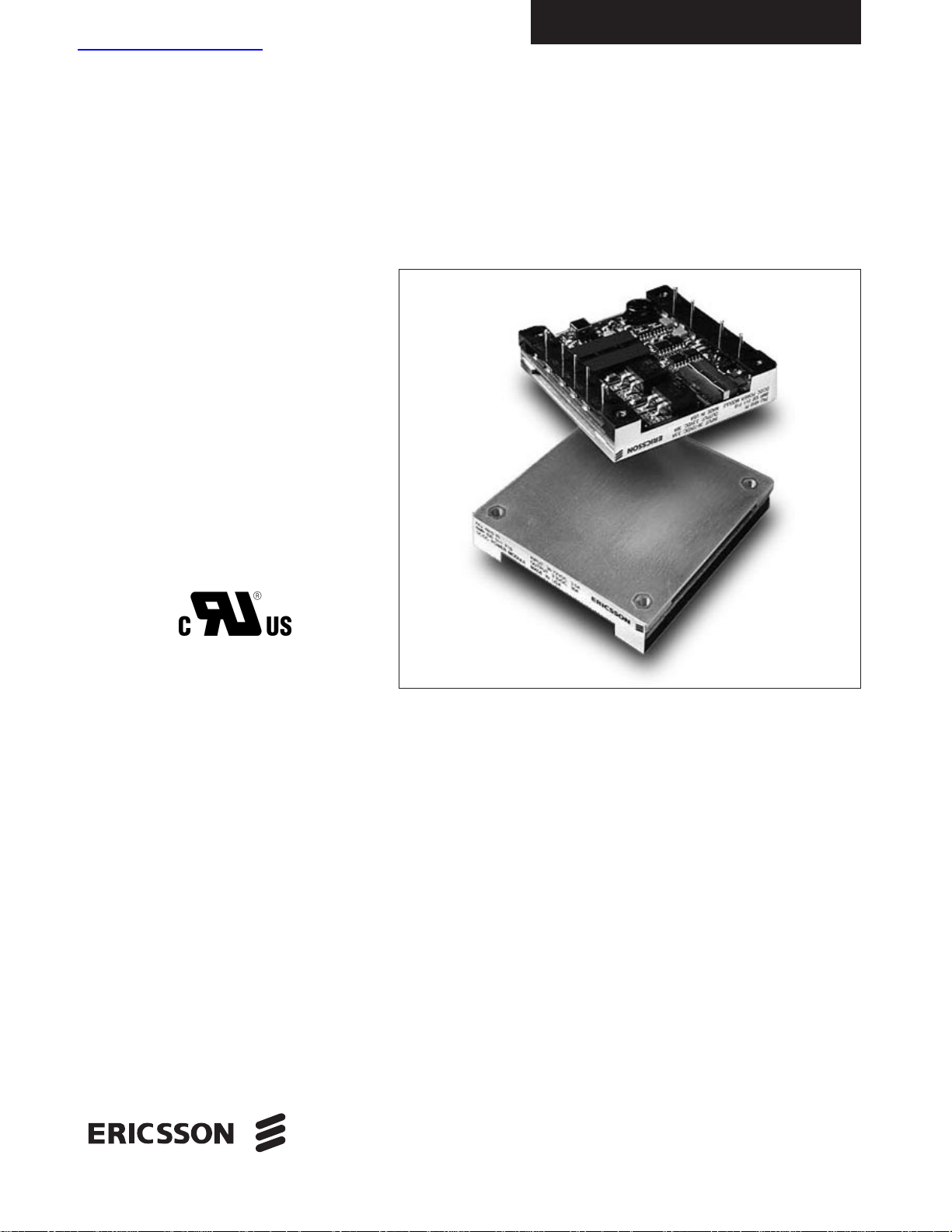
The PKJ series represents a “third generation” of High
Density DC/DC Power Modules providing 90% efficiency.
To achieve this high efficiency, Ericsson uses proprietary drive
and control circuits with planar magnetics and low resistivity
multilayer PCB technology, and a patent pending topology
with active rectification. The PKJ series can be used without
bulky and height consuming heatsinks, resulting in a lower
total cost. This also provides narrow board spacing for electronic, shelf based applications.
The products are in the industry standard package size and
offer a beneficial alternative to competing products on the
market. Because for certain applications they may not
require heatsinks, they are ideal for cost sensitive or highdensity applications.
The PKJ series also offers the flexibility of using a heatsink
when needed, enabling reduced airflow, extended reliability
or higher ambient temperature operation in a wide range of
48V and 60V DC powered systems. Similar to other
Ericsson Power Modules, the PKJ series includes an undervoltage shut down facility, protecting the associated batteries from being too deeply discharged. The PKJ series also
offers over-voltage protection, over-temperature protection
and is short circuit proof.
These products are manufactured using highly automated
manufacturing lines with a world-class quality commitment
and a five-year warranty. Ericsson Components AB has been
an ISO 9001 certified supplier since 1991. For product
program please see back cover.
查询PKJ4111API供应商
Page 2

Data Sheet AE/LZT 137 57 R1 © Ericsson Components AB, August 1999
Characteristics min max Unit
TCMaximum Operating Case Temperature -40 +100 °C
TSStorage temperature -40 +125 °C
VIContinuous input voltage -0.5 +75 Vdc
V
ISO
Isolation voltage 1,500 Vdc
(input to output test voltage)
V
RC
Remote control voltage 15 Vdc
I2t Inrush transient 1 A2s
Characteristics Conditions min typ max Unit
V
I
Input voltage 36 72 Vdc
range
1)
V
Ioff
Turn-off input Ramping from 31 33 Vdc
voltage higher voltage
V
Ion
Turn-on input Ramping from 34 36 Vdc
voltage lower voltage
C
I
Input capacitance 2.8 µF
I
Iac
Reflected 5 Hz to 20 MHz-150W 20 mA p-p
ripple current
50 W 1.6
I
I
max Maximum input V
I
= V
I
min 75 W 2.4 A
current 100 W 3.2
150 W 5.3
P
Ii
Input idling power IO= 0 2.5 7.5 W
P
RC
Input
stand-by power V
I
= 50V RC open .05 2.5 W
(turned off with RC)
TRIM Maximum input 6 Vdc
voltage on trim pin
Characteristics Test procedure & conditions
Random IEC 68-2-34EdFrequency 10...500 Hz
Vibration Spectral density 0.025 g2/Hz
Duration 10 min in each
direction
Sinusoidal IEC 68-2-6 F
c
Frequency 10-500 Hz
Vibration Amplitude 0.75mm
Acceleration 10g
# of cycles 10 in each axis
Shock IEC 68-2-27 E
a
Peak acceleration 50 g
(half sinus) Duration 3ms
Temperature IEC 68-2-14 N
a
Temperature -40°C...+100°C
change Number of cycles 300
Accelerated IEC 68-2-3 C
a
Temperature 85°C
damp heat with bias Humidity 85% RH
Duration 500 hours
Solder IEC 68-2-20 T
b
Temperature, solder 260° C
resistibility method IA Duration 10...13 s
General
Absolute Maximum Ratings
Input
TC < T
Cmax
Environmental Characteristics
2
Stress in excess of Absolute Maximum Ratings may
cause permanent damage. Absolute Maximum Ratings,
sometimes referred to as no destruction limits, are
normally tested with one parameter at a time exceeding
the limits of Output data or Electrical Characteristics.
If exposed to stress above these limits, function and
performance may degrade in an unspecified manner.
For design margin and to enhance system reliability,
it is recommended that the PKJ series DC/DC power
modules are operated at case temperatures below 90°C.
1) See also Input Voltage in the Operating
Information section
Safety
The PKJ Series DC/DC power modules are
designed to comply with EN 60 950 Safety of
information technology equipment including
electrical business equipment.
The PKJ DC/DC power modules are also
recognized by UL and meet the applicable
requirements in UL 1950, Safety of information
technology equipment and applicable Canadian
safety requirements.
The isolation is an operational insulation in
accordance with EN 60 950. The DC/DC power
module should be installed in end-use equipment,
in compliance with the requirements of the
ultimate application, and is intended to be
supplied by an isolated secondary circuit.
Consideration should be given to measuring
the case temperature to comply with T
C
max
when in operation.
When the supply to the DC/DC power
module meets all the requirements for SELV
(<60Vdc), the output is considered to remain
within SELV limits (level 3). If connected to a 60V
DC power system, reinforced insulation must be
provided in the power supply that isolates the
input from the mains. Single fault testing in the
power supply must be performed in combination
with the DC/DC power module to demonstrate
that the output meets the requirement for SELV.
One pole of the input and one pole of the output
is to be grounded or both are to be kept floating.
Page 3
3
Data Sheet AE/LZT 137 57 R1 © Ericsson Components AB, August 1999
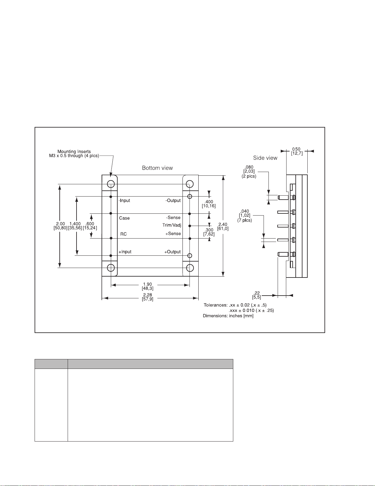
Designation Function
-In Negative input
Case Connected to base plate
RC Remote control (primary). To turn-on
and turn-off the output
+In Positive input
-Out Negative output
-Sen Negative remote sense (if sense not needed, connect to -Out)
Trim Output voltage adjust
+Sen Positive remote sense (if sense not needed, connect to +Out)
+Out Positive output
Connections
Weight
85 grams
Case
Aluminum baseplate with metal standoffs.
Pins
Pin material: Brass
Pin plating: Tin/Lead over Nickel.
Mechanical Data
Safety (continued)
The galvanic isolation is verified in an electric strength test. The
test voltage (V
ISO
) between input and output is 1,500 Vdc for
60 sec. Leakage current is less than 1
µA @ 50Vdc.
Flammability ratings of the terminal support and internal plastic
construction details meet UL 94V-0.
A fuse should be used at the input of each PKJ series power module.
If a fault occurs in the power module, that imposes a short on the
input source, this fuse will provide the following two functions:
• Isolate the failed module from the input source so that the
remainder of the system may continue operation.
• Protect the distribution wiring from
overheating.
A fast blow fuse should be used with a rating of 10A or less. It is
recommended to use a fuse with the lowest current rating, that is
suitable for the application.
Page 4
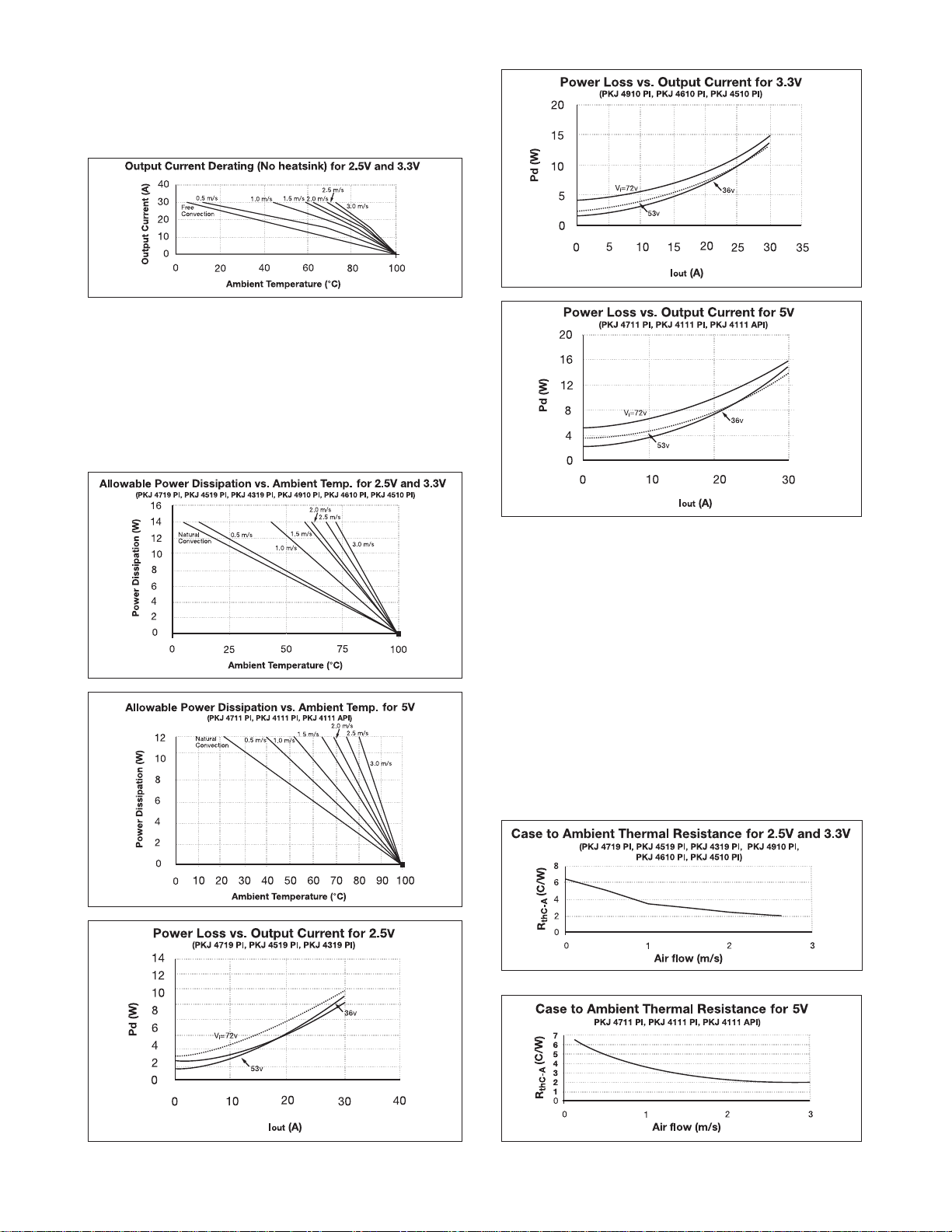
Thermal Data
The PKJ series DC/DC power modules has a robust thermal design
which allows operation at case (baseplate) temperatures (T
C
) up to
+100°C. The main cooling mechanism is convection (free or forced)
through the case or optional heatsinks.
The graph above shows the allowable maximum output
current to maintain a maximum +100°C case temperature.
Note that the ambient temperature is the air temperature
adjacent to the power module which is typically elevated
above the room environmental temperature.
The graphs below can be used to estimate case temperatures
for given system operating conditions (see Thermal design).
For further information on optional heatsinks, please contact
your local Ericsson sales office.
Thermal Design
The thermal data can be used to determine thermal performance
without a heatsink.
Case temperature is calculated by the following formula:
T
C
= TA+ Pdx R
thC-A
where Pd= P
O
(1/η - 1)
Where:
T
C
: Case Temperature
T
A
: Local Ambient Temperature
P
d
: Dissipated Power
R
thC-A
: Thermal Resistance from TCto T
A
The efficiency η can be found in the tables on the following pages.
For design margin and to enhance system reliability, it is recommended that the PKJ series DC/DC power modules are operated at case
temperatures below 90°C.
4
Data Sheet AE/LZT 137 57 R1 © Ericsson Components AB, August 1999
Page 5

5
Data Sheet AE/LZT 137 57 R1 © Ericsson Components AB, August 1999
Characteristics Conditions Output
min typ max Unit
V
Oi
Output voltage initial TC= +25°C, VI= 53V, IO= I
O
max 2.45 2.5 2.55 V
setting and accuracy
Output adjust range IO= 0 to I
O
max 2.0 2.75 V
V
O
Output voltage IO= 0 to I
O
max 2.38 2.63 V
tolerance band
Line regulation VI= 36...72V, IO= I
O
max 2 15 mV
Load regulation VI= 53V, IO= 0 to I
O
max 2 15 mV
V
tr
Load transient Load step = 0.25 x I
O
max
±
160 mVpeak
voltage deviation dI/dt = 1A/µs
t
tr
Load transient 50 µs
recovery time
t
s
Start-up time From VIconnection to VO= 0.9 x V
O
nom 35 55 ms
I
O
Output current 0 30 A
P
O
max Max output power At V
O
= V
O
nom 75 W
I
lim
Current limit threshold VO= 0.90 x V
O
nom @ T
C
<100°C 31 35 41 A
I
SC
Short circuit current 35 41 A
VOac Output ripple and noise IO= I
O
max f < 20 MHz 75 150 mVp-p
SVR Supply voltage f<1 kHz -53 dB
rejection
OVP Overvoltage protection 3.0 3.3 3.9 V
Output
PKJ 4719 PI (75W)
TC= -40...+100°C, VI= 36...72 V dc unless otherwise specified.
Characteristics Conditions min typ max Unit
η Efficiency TA= +25°C, VI= 53V, IO= I
O
max 84 87 %
P
d
Power dissipation IO= I
O
max, V
I
= 53V 11.2 W
f
O
Switching frequency IO= 0.1...1.0 x I
O
max 150 kHz
Miscellaneous
Page 6

Characteristics Conditions Output
min typ max Unit
V
Oi
Output voltage initial TC= +25°C, VI= 53V, IO= I
O
max 2.45 2.50 2.55 V
setting and accuracy
Output adjust range IO= 0 to I
O
max 2.0 2.75 V
V
O
Output voltage IO= 0 to I
O
max 2.38 2.63 V
tolerance band
Line regulation VI= 36...72VIO= 0 to I
O
max 2 15 mV
Load regulation VI= 53V, IO= 0 to I
O
max 2 15 mV
V
tr
Load transient Load step = 0.25 x I
O
max ±100 mVpeak
voltage deviation dI/dt = 1A/µs
t
tr
Load transient 50 µs
recovery time
t
s
Start-up time From VIconnection to VO= 0.9 x V
O
nom 30 55 ms
I
O
Output current 0 20 A
P
O
max Max output power At V
O
= V
O
nom 50 W
I
Iim
Current limit threshold VO= 0.90 x V
O
nom @ T
C
<100°C 21 25 31 A
I
SC
Short circuit current 25 31 A
VOac Output ripple and noise IO= I
O
max f < 20 MHz 75 150 mVp-p
SVR Supply voltage f<1 kHz -53 dB
rejection
OVP Overvoltage protection 3.0 3.3 3.9 V
Output
PKJ 4519 PI (50W)
TC= -40...+100°C, VI= 36...72 V dc unless otherwise specified.
6
Data Sheet AE/LZT 137 57 R1 © Ericsson Components AB, August 1999
Characteristics Conditions min typ max Unit
η Efficiency TA= +25°C, VI= 53V, IO= I
O
max 86 89 %
P
d
Power dissipation IO= I
O
max, V
I
= 53V 6.2 W
f
O
Switching frequency IO= 0.1...1.0 x I
O
max 150 kHz
Miscellaneous
Page 7

7
Data Sheet AE/LZT 137 57 R1 © Ericsson Components AB, August 1999
Characteristics Conditions Output
min typ max Unit
V
Oi
Output voltage initial TC= +25°C, VI= 53V, IO= I
O
max 2.45 2.50 2.55 V
setting and accuracy
Output adjust range IO= 0 to I
O
max 2.0 2.75 V
V
O
Output voltage IO= 0 to I
O
max 2.38 2.63 V
tolerance band
Line regulation VI= 36...72V, IO= I
O
max 2 15 mV
Load regulation VI= 53V, IO= 0 to I
O
max 2 15 mV
V
tr
Load transient Load step = 0.25 x I
O
max ±90 mVpeak
voltage deviation dI/dt = 1A/µs
t
tr
Load transient 50 µs
recovery time
t
S
Start-up time From VIconnection to VO= 0.9 x V
O
nom 30 55 ms
I
O
Output current 0 15 A
P
O
max Max output power At V
O
= V
O
nom 37.5 W
I
Iim
Current limit threshold VO= 0.90 x V
O
nom @ T
C
<100°C 16 17 24 A
I
SC
Short circuit current 17 25 A
VOac Output ripple and noise IO= I
O
max f <20 MHz 75 150 mVp-p
SVR Supply voltage f<1 kHz 53 dB
rejection
OVP Overvoltage protection 3.0 3.3 3.9 V
Output
PKJ 4319 PI (37.5W)
TC= -40...+100°C, VI= 36...72 V dc unless otherwise specified.
Characteristics Conditions min typ max Unit
η Efficiency TA= +25°C, VI= 53V, IO= I
O
max 86 89 %
P
d
Power dissipation IO= I
O
max, V
I
= 53V 4.6 W
f
O
Switching frequency IO= 0.1...1.0 x I
O
max 150 kHz
Miscellaneous
Page 8

Characteristics Conditions Output
min typ max Unit
V
Oi
Output voltage initial TC= +25°C, VI= 53V, IO= I
O
max 3.25 3.30 3.35 V
setting and accuracy
Output adjust range IO= 0 to I
O
max 2.64 3.63 V
V
O
Output voltage IO= 0 to I
O
max 3.2 3.4 V
tolerance band
Line regulation VI= 36...72V, IO= I
O
max 1 10 mV
Load regulation VI= 53V, IO= 0 to I
O
max 1 10 mV
V
tr
Load transient Load step = 0.25 x I
O
max ±180 mV
peak
voltage deviation dI/dt = 1A/µs
t
tr
Load transient 50 µs
recovery time
t
S
Start-up time From VIconnection to VO= 0.9 x V
O
nom 35 60 ms
I
O
Output current 0 30 A
P
O
max Max output power At V
O
= V
O
nom 100 W
I
Iim
Current limit threshold VO= 0.90 x V
O
nom @ T
C
<100°C 31 35 39 A
I
SC
Short circuit current 35 41 A
V
Oac
Output ripple and noise IO= I
O
max f <20 MHz 75 150 mVp-p
SVR Supply voltage f<1kHz -53 dB
rejection (ac)
OVP Over voltage protection VI= 53V 3.9 4.4 5.0 V
Output
PKJ 4910 PI (99W)
TC= -40...+100°C, VI= 36...72 V dc unless otherwise specified.
8
Data Sheet AE/LZT 137 57 R1 © Ericsson Components AB, August 1999
Characteristics Conditions min typ max Unit
η Efficiency TA= +25°C, VI= 53V, IO= I
O
max 86 89 %
P
d
Power dissipation IO= I
O
max, V
I
= 50V 12.2 W
f
O
Switching frequency IO= 0.1...1.0 x I
O
max 150 kHz
Miscellaneous
Page 9

9
Data Sheet AE/LZT 137 57 R1 © Ericsson Components AB, August 1999
PKJ 4610 PI (66W)
TC= -40...+100°C, VI= 36...72 V dc unless otherwise specified.
Characteristics Conditions Output
min typ max Unit
V
Oi
Output voltage initial TC= +25°C, VI= 53V, IO= I
O
max 3.25 3.30 3.35 V
setting and accuracy
Output adjust range IO= 0 to I
O
max 2.64 3.63 V
V
O
Output voltage IO= 0 to I
O
max 3.2 3.4 V
tolerance band
Line regulation VI= 36...72V, IO= I
O
max 1 10 mV
Load regulation VI= 53V, IO= 0 to I
O
max 1 10 mV
V
tr
Load transient Load step = 0.25 x I
O
max ±140 mV
peak
Voltage deviation dI/dt = 1A/µs
t
tr
Load transient 50 µs
recovery time
t
s
Start-up time From VIconnection to VO= 0.9 x V
O
nom 35 60 ms
I
O
Output current 0 20 A
P
O
max Max output power At V
O
= V
O
nom 66.6 W
I
Iim
Current limit threshold VO= 0.90 x V
O
nom @ T
C
<100°C 21 24 30 A
I
SC
Short circuit current 28 32 A
V
Oac
Output ripple and noise IO= I
O
max f <20 MHz 75 150 mVp-p
SVR Supply voltage f<1kHz -53 dB
rejection (ac)
OVP Over voltage protection 3.9 4.4 5.0 V
Output
Characteristics Conditions min typ max Unit
η Efficiency TA= +25°C, VI= 53V, IO= I
O
max 88 90.5 %
P
d
Power dissipation IO= I
O
max, V
I
= 53V 6.93 W
f
O
Switching frequency IO= 0.1...1.0 x I
O
max 150 kHz
Miscellaneous
Page 10

PKJ 4510 PI (50W)
TC= -40...+100°C, VI= 36...72 V dc unless otherwise specified.
Characteristics Conditions Output
min typ max Unit
V
Oi
Output voltage initial TC= +25°C, VI= 53V, IO= I
O
max 3.25 3.30 3.35 V
setting and accuracy
Output adjust range IO= 0 to I
O
max 2.64 3.63 V
V
O
Output voltage IO= 0 to I
O
max 3.2 3.4 V
tolerance band
Line regulation VI= 36...72V, IO= I
O
max 1 10 mV
Load regulation VI= 53V, IO= 0 to I
O
max 1 10 mV
V
tr
Load transient Load step = 0.25 x I
O
max ±100 mV
peak
Voltage deviation dI/dt = 1A/µs
t
tr
Load transient 50 µs
recovery time
t
s
Start-up time From VIconnection to VO= 0.9 x V
O
nom 35 60 ms
I
O
Output current 0 15 A
P
O
max Max output power At V
O
= V
O
nom 50 W
I
Iim
Current limit threshold VO= 0.90 x V
O
nom @ T
C
<100°C 16 19 22 A
I
SC
Short circuit current 21 23 A
V
Oac
Output ripple and noise IO= I
O
max f < 20 MHz 75 150 mVp-p
SVR Supply voltage f<1kHz -53 dB
rejection (ac)
OVP Over voltage protection 3.9 4.4 5.0 V
Output
10
Data Sheet AE/LZT 137 57 R1 © Ericsson Components AB, August 1999
Characteristics Conditions min typ max Unit
η Efficiency TA= +25°C, VI= 53V, IO= I
O
max 88 90.5 %
P
d
Power dissipation IO= I
O
max, V
I
= 53V 5.2 W
f
O
Switching frequency IO= 0.1...1.0 x I
O
max 150 kHz
Miscellaneous
Page 11

11
Data Sheet AE/LZT 137 57 R1 © Ericsson Components AB, August 1999
Characteristics Conditions Output
min typ max Unit
V
Oi
Output voltage initial TC= +25°C, VI= 53V, IO= I
O
max 4.9 5.0 5.1 V
setting and accuracy
Output adjust range IO= 0.1 to I
O
max 4.0 5.5 V
V
O
Output voltage IO= 0.1 to I
O
max 4.85 5.15 V
tolerance band
Line regulation VI= 36...72V, IO= I
O
max 5 20 mV
Load regulation VI= 53V, IO= 0.1 to I
O
max 5 20 mV
V
tr
Load transient Load step = 0.25 x I
O
max ±200 mV
peak
voltage deviation dI/dt = 1A/µs
t
tr
Load transient 50 µs
recovery time
t
s
Start-up time From VIconnection to VO= 0.9 x V
O
nom 55 90 ms
I
O
Output current 0 30 A
P
O
max Max output power At V
O
= V
O
nom 150 W
I
Iim
Current limit threshold VO= .90 x V
O
nom @ T
C
<100°C 31 35 42 A
I
SC
Short circuit current 35 41 A
VOac Output ripple and noise IO= I
O
max f < 20 MHz 75 150 mVp-p
SVR Supply voltage f<1 kHz -53 dB
rejection (ac)
OVP Over voltage protection 5.8 6.1 7 V
Output
PKJ 4111 API (150W)
TC= -40...+100°C, VI= 36...72 V dc unless otherwise specified.
Characteristics Conditions min typ max Unit
η Efficiency TA= +25°C, VI= 53V, IO= I
O
max 88 90.5 %
P
d
Power dissipation IO= I
O
max, V
I
= 53V 15.7 W
f
O
Switching frequency IO= 0.1...1.0 x I
O
max 200 kHz
Miscellaneous
Page 12

Characteristics Conditions Output
min typ max Unit
V
Oi
Output voltage initial TC= +25°C, VI= 53V, IO= I
O
max 4.9 5.0 5.1 V
setting and accuracy
Output adjust range IO= 0 to I
O
max 4.0 5.5 V
V
O
Output voltage IO= 0 to I
O
max 4.85 5.15 V
tolerance band
Line regulation VI= 36...72V, IO= I
O
max 5 20 mV
Load regulation VI= 53V, IO= 0.1 to I
O
max 5 20 mV
V
tr
Load transient Load step = 0.25 x I
O
max ±120 mV
peak
voltage deviation dI/dt = 1A/µs
t
tr
Load transient 20 µs
recovery time
t
s
Start-up time From VIconnection to VO= 0.9 x V
O
nom 55 90 ms
I
O
Output current 0 20 A
P
O
max Max output power At V
O
= V
O
nom 100 W
I
Iim
Current limiting threshold VO= 0.90 x V
O
nom @ T
C
<100°C 21 25 32 A
I
SC
Short circuit current 25 31 A
VOac Output ripple and noise IO= I
O
max f < 20 MHz 75 150 mVp-p
SVR Supply voltage f<1 kHz -53 dB
rejection (ac)
OVR Over voltage protection 5.8 6.1 7 V
Output
PKJ 4111 PI (100W)
TC= -40...+100°C, VI= 36...72 V dc unless otherwise specified.
12
Data Sheet AE/LZT 137 57 R1 © Ericsson Components AB, August 1999
Characteristics Conditions min typ max Unit
η Efficiency TA= +25°C, VI= 53V, IO= I
O
max 89 91.5 %
P
d
Power dissipation IO= I
O
max, V
I
= 53V 9.3 W
f
O
Switching frequency IO= 0.1...1.0 x I
O
max 200 kHz
Miscellaneous
Page 13

13
Data Sheet AE/LZT 137 57 R1 © Ericsson Components AB, August 1999
Characteristics Conditions Output
min typ max Unit
V
Oi
Output voltage initial TC= +25°C, VI= 53V, IO= I
O
max 4.9 5.0 5.1 V
setting and accuracy
Output adjust range IO= 0 to I
O
max 4.0 5.5 V
V
O
Output voltage IO= 0 to I
O
max 4.85 5.15 V
tolerance band
Line regulation VI= 36...72V, IO= I
O
max 5 20 mV
Load regulation VI= 53V, IO= 0.1 to I
O
max 5 20 mV
V
tr
Load transient Load step = 0.25 x I
O
max ±100 mV
peak
voltage deviation dI/dt = 1A/µs
t
tr
Load transient 15 µs
recovery time
t
s
Start-up time From VIconnection to VO= 0.9 x V
O
nom 55 90 ms
I
O
Output current 0 15 A
P
O
max Max output power At V
O
= V
O
nom 75 W
I
Iim
Current limiting threshold VO= 0.90 x V
O
nom @ T
C
<100°C 16 20 26 A
I
SC
Short circuit current 22 25 A
VOac Output ripple and noise IO= I
O
max f < 20 MHz 75 150 mVp-p
SVR Supply voltage f† 1 kHz -53 dB
rejection (ac)
OVP Over voltage protection 5.8 6.1 7 V
Output
PKJ 4711 PI (75W)
TC= -40...+100°C, VI= 36...72 V dc unless otherwise specified.
Characteristics Conditions min typ max Unit
η Efficiency TA= +25°C, VI= 53V, IO= I
O
max 89 91.5 %
P
d
Power dissipation IO= I
O
max, V
I
= 53V 7.0 W
f
O
Switching frequency IO= 0.1...1.0 x I
O
max 200 kHz
Miscellaneous
Page 14

Typical Characteristics
PKJ 4719 PI (75W)
PKJ 4519 PI (50W)
PKJ 4319 PI (37.5W)
14
Data Sheet AE/LZT 137 57 R1 © Ericsson Components AB, August 1999
Page 15

15
Data Sheet AE/LZT 137 57 R1 © Ericsson Components AB, August 1999
PKJ 4910 PI (99W)
PKJ 4610 PI (66W)
PKJ 4510 PI (50W)
4
2
3
1
4
2
3
1
4
2
3
1
Page 16

PKJ 4111 API (150W)
PKJ 4111 PI (100W)
PKJ 4711 PI (75W)
16
Data Sheet AE/LZT 137 57 R1 © Ericsson Components AB, August 1999
Page 17

17
Data Sheet AE/LZT 137 57 R1 © Ericsson Components AB, August 1999
EMC Specifications
The PKJ power module is mounted on a double sided printed circuit board PCB with groundplane during EMC
measurements.
The fundamental switching frequency is 200 kHz @ I
O
= I
O
max.
Conducted EMI
Input terminal value with 100µF capacitor (typ) and additional PI filter.
dBuV
0.15MHz
30MHz
EMI Filter for PKJ Module
1.0MHz
10MHz
L1: 425µH, 8.1A (Coilcraft P3217A)
L2: 22µH, 7A (Coilcraft D055022-223)
Page 18

Remote Sense
All PKJ series DC/DC power modules have remote sense that can
be used to compensate for moderate amounts of resistance in the
distribution system and allow for voltage regulation at the load or
other selected point. The remote sense lines will carry very little
current and do not need a large cross sectional area. However, the
sense lines on a PCB should be located close to a ground trace or
ground plane. In a discrete wiring situation, the usage of twisted pair
wires or other technique for reducing noise susceptibility is
recommended.
The power module will compensate for up to 0.5 V voltage drop
between the sense voltage and the voltage at the power module
output pins. The output voltage and the remote sense voltage
offset must be less than the minimum overvoltage trip point.
If the remote sense is not needed the -Sen should be connected
to -Out and +Sen should be connected to +Out.
Current Limiting
General Characteristics
All PKJ series DC/DC power modules include current limiting circuitry
that makes them able to withstand continuous overloads or short circuit
conditions on the output. The output voltage will decrease toward zero
for heavy overloads (see product code characteristics).
The power module will resume normal operation after removal of the
overload. The load distribution system should be designed to carry
the maximum short circuit output current specified (see applicable
code typical characteristics).
Over Voltage Protection (OVP)
All PKJ DC/DC power modules have latching output overvoltage
protection. In the event of an overvoltage condition, the power module will shut down. The power module can be restarted by cycling
the input voltage.
Turn-off Input Voltage (V
I
off)
The power module monitors the input voltage and will turn on and
turn off at predetermined levels.
Operating Information
Input Voltage
The input voltage range 36...72V meets the requirements in the
European Telecom Standard ETS 300 132-2 for normal input voltage
range in -48 V and -60 V DC power systems, -40.5...-57.0 V and
-50.0...-72.0 V respectively. At input voltages exceeding 72 V,
(abnormal voltage), the power loss will be higher than at normal
input voltage and T
C
must be limited to absolute max +90º C. The
absolute max continuous input voltage is 75 V DC. Output characteristics will be marginally affected at input voltages exceeding 72 V.
Remote Control (RC)
The RC pin can be wired directly to -In, to allow the module to
power up automatically without the need for control signals.
A mechanical switch or an open collector transistor or FET can be
used to drive the RC inputs. The device must be capable of sinking
up to 1mA at a low level voltage of 1.0V, maximum of 15 V dc, for
the primary RC.
RC (primary) Power module
Low ON
Open/High OFF
Output Voltage Adjust (Trim)
Voltage Trimming
All PKJ series DC/DC power modules have an Output Voltage
Adjust pin. This pin can be used to adjust the output voltage
above or below V
Oi
. When increasing the output voltage, the
voltage at the output pins (including any remote sensing offset)
must be kept below the overvoltage trip point. Also note that
at elevated output voltages the maximum power rating of the
module remains the same, and the output current capability will
decrease correspondingly.
To decrease V
O
connect Radj from - SEN to Trim
To increase V
O
connect Radj from + SEN to Trim
Decrease : Radj = (21*V
O
-2.5)/(2.5-VO) k ohm
Increase : Radj = (9.7*V
O
+1.225)/(0.49*VO-1.225) k ohm
Decrease : Radj = (11V
O
-3.3)/(3.3-VO) k ohm
Increase : Radj = 15.94*(V
O
+0.207)/(VO-3.3) k ohm
Decrease : Radj = (11V
O
-4.965)/(4.965-VO) k ohm
Increase : Radj = (7.286*V
O
+1.225)/(0.2467*VO-1.225) k ohm
18
Data Sheet AE/LZT 137 57 R1 © Ericsson Components AB, August 1999
Standard Remote Control
RC (primary) Power module
Low OFF
Open/High ON
Optional Remote Control
Page 19

Paralleling for Redundancy
The figure below shows how n + 1 redundancy can be achieved.
The diodes on the power module outputs allow a failed module
to remove itself from the shared group without pulling down the common output bus. This configuration can be extended to
additional numbers of power modules and they can also be
controlled individually or in groups by means of signals to the
primary RC inputs.
Output Ripple & Noise (V
O
ac
)
Output ripple is measured as the peak to peak voltage from 0 to
20MHz which includes the noise voltage and fundamental.
Over Temperature Protection
The PKJ DC/DC power modules are protected from thermal overload
by an internal over temperature shutdown circuit. When the case
temperature exceeds +110°C, the power module will automatically
shut down (latching). To restart the module the input voltage must
be cycled. The internal temperature is a few degrees higher than the
case (baseplate) temperature.
Input and Output Impedance
The impedance of both the power source and the load will interact
with the impedence of the DC/DC power module. It is most important
to have the ratio between L and C as low as possible, i.e. a low characteristic impedance, both at the input and output, as the power modules have a low energy storage capability. The PKJ series of DC/DC
power modules has been designed to be completely stable without the
need for external capacitors on the input or output when configured
with low inductance input and output circuits. The performance in
some applications can be enhanced by the addition of external capacitance as described below. If the distribution of the input voltage source
to the power module contains significant inductance, the addition of a
220-470 µF capacitor across the input of the power module will help
insure stability. Tantalum capacitors are not recommended due to their
low ESR-value. This capacitor is not required when powering the
module from a low impedance source with short, low inductance,
input power leads.
Output Capacitance
When powering loads with significant dynamic current requirements,
the voltage regulation at the load can be improved by the addition of
decoupling capacitance at the load. The most effective technique is to
locate low ESR ceramic capacitors as close to the load as possible, using
several capacitors to lower the effective ESR. These ceramic capacitors
will handle the short duration high frequency components of the
dynamic current requirement. In addition, higher values of electrolytic
capacitors should be used to handle the mid frequency components. It
is equally important to use good design practices when configuring the
DC distribution system.
19
Data Sheet AE/LZT 137 57 R1 © Ericsson Components AB, August 1999
Low resistance and low inductance PCB (printed circuit board) layouts
and cabling should be used. Remember that when using remote sensing, all the resistance, inductance and capacitance of the distribution
system is within the feedback loop of the power module. This can have
an effect on the modules compensation and the resulting stability and
dynamic response performance.
As a rule of thumb, 100 µF/A of output current can be used without
any additional analysis. For example, with a 30A (max P
O
150W)
power module, values of decoupling capacitance up to 3000 µF can be
used without regard to stability. With larger values of capacitance, the
load transient recovery time can exceed the specified value. As much of
the capacitance as possible should be outside of the remote sensing
loop and close to the load.The absolute maximum value of output
capacitance is 10,000 µF. For values larger than this contact your local
Ericsson representative.
Quality
Reliability
The calculated MTBF of the PKJ module family is 3 million
hours using Bellcore TR-332 methodology. The calculation is valid
for an ambient temperature of 40°C and an output load 80% of
rated maximum.
Quality Statement
The power modules are designed and manufactured in an industrial
environment where quality systems and methods like ISO 9000, 6σ,
and SPC, are intensively in use to boost the continuous improvements
strategy. Infant mortality or early failures in the products are screened
out and they are subjected to an ATE-based final test.
Conservative design rules, design reviews and product qualifications,
plus the high competence of an engaged work force, contribute to the
high quality of our products.
Warranty
Ericsson Components warrants to the original purchaser or end user
that the products conform to this Data Sheet and are free from material
and workmanship defects for a period of five (5) years from the date of
manufacture, if the product is used within specified conditions and not
opened.
In case the product is discontinued, claims will be accepted up to three
(3) years from the date of the discontinuation. For additional details on
this limited warranty we refer to Ericsson Components AB’s “General
Terms and Conditions of Sales”, EKA 950701, or individual contract
documents.
Limitation of Liability
Ericsson Components does not make any other warranties, expressed
or implied including any warranty of merchantability or fitness for a
particular purpose (including, but not limited to use in life support
applications, where malfunctions of product can cause injury to a
person’s health or life).
Page 20

Ericsson Energy Systems’ Sales Offices:
Brazil: Phone: +55 11 681 0040 Fax: +55 11 681 2051
Denmark: Phone: +45 33 883 109 Fax: +45 33 883 105
Finland: Phone: +358 9 299 4098 Fax: +358 9 299 4188
France: Phone: +33 1 4083 7720 Fax: +33 1 4083 7741
Germany: Phone: +49 211 534 1516 Fax: +49 211 534 1525
Great Britain: Phone: +44 1793 488 300 Fax: +44 1793 488 301
Hong Kong: Phone: +852 2590 2356 Fax: +852 2590 7152
Italy: Phone: +39 2 7014 4203 Fax: +39 2 7014 4260
Japan: Phone: +81 3 5216 9091 Fax: +81 3 5216 9096
Norway: Phone: +47 66 841 906 Fax: +47 66 841 909
Russia: Phone: +7 095 247 6211 Fax: +7 095 247 6212
Spain: Phone: +34 91 339 1858 Fax: +34 91 339 3145
Sweden: Phone: +46 8 721 6258 Fax: +46 8 721 7001
United States: Phone: +1 888 853 6374 Fax: +1 972 583 7999
Ericsson Components AB
Energy Systems Division
SE-164 81 Kista-Stockholm, Sweden
Phone: +46 8 721 6258 Fax: +48 8 721 7001
Internet: www.ericsson.com/energy
Information given in this data sheet is believed
to be accurate and reliable. No respnsibility is
assumed for the consequences of its use nor for
any infringement of patents or other rights of
third parties which may result from its use. No
license is granted by implication or otherwise
under any patent or patent rights of Ericsson
Components. These products are sold only
according to Ericsson Components’ general
conditions of sale, unless otherwise confirmed
in writing.
Specifications subject to change without notice.
Preliminary Data Sheet
AE/LZT 137 57 R1
© Ericsson Components AB, August 1999
V
I
VO/I
O
P
O
max Ordering Number
48/60 V 2.5V/30A 75W PKJ 4719 PI
48/60 V 2.5V/20A 50W PKJ 4519 PI
48/60 V 2.5V/15A 37.5W PKJ 4319 PI
48/60 V 3.3V/30A 100W PKJ 4910 PI
48/60 V 3.3V/20A 66W PKJ 4610 PI
48/60 V 3.3V/15A 50W PKJ 4510 PI
48/60 V 5V/30A 150W PKJ 4111 API
48/60 V 5V/20A 100W PKJ 4111 PI
48/60 V 5V/15A 75W PKJ 4711 PI
Product Program
To order with Optional Remote Control add P to end of ordering number for
example PKJ 4719 PIP.
 Loading...