

Ericsson PBL40310 Datasheet
Advance information
PBL 40310
PBL 403 10
March 2001
PBL 403 10
3.5 V GSM 900 MHz Power Amplifier
Description.
The PBL 40310 is a highly integrated single-ended silicon MMIC power amplifier
intended for use in GSM terminals. It delivers 35 dBm at 900 MHz with 55 % power added
efficiency into a 50 Ω unbalanced load using a single 3.5 V supply.
The circuit has an analog ramp signal to control output power level and a logical on/
off signal for power down mode. It can be used in dual-band amplifiers using the band
select logical signal. It can be operated up to 50 % duty cycle with minimum performance
degradation. The circuit is housed in a specially designed QSOP16 (150 mil body)
package and the implementation requires only few external components.
25 GHz ft state-of-the-art deep trench isolated double-poly silicon bipolar process
with additional features for improved wireless performance has been used. On-chip
capacitors and inductors are used for the integrated internal matching network. Special
front-side metallized substrate contacts provide excellent ground paths from active
devices to the highly doped semiconductor substrate and package ground.
V
CC
Key features.
• 2.7 to 5.0 V single supply operation
• 35 dBm output power at 3.5 V
• 55 % Power Added Efficiency
• Input matched to 50 Ω
• Complete on chip input and
interstage matching
• Analog power control
• Less than 10 µA current
consumption in power down mode
• Proven RF Silicon Technology
Reliability
• Minimum number of external
components for low overall solution
cost
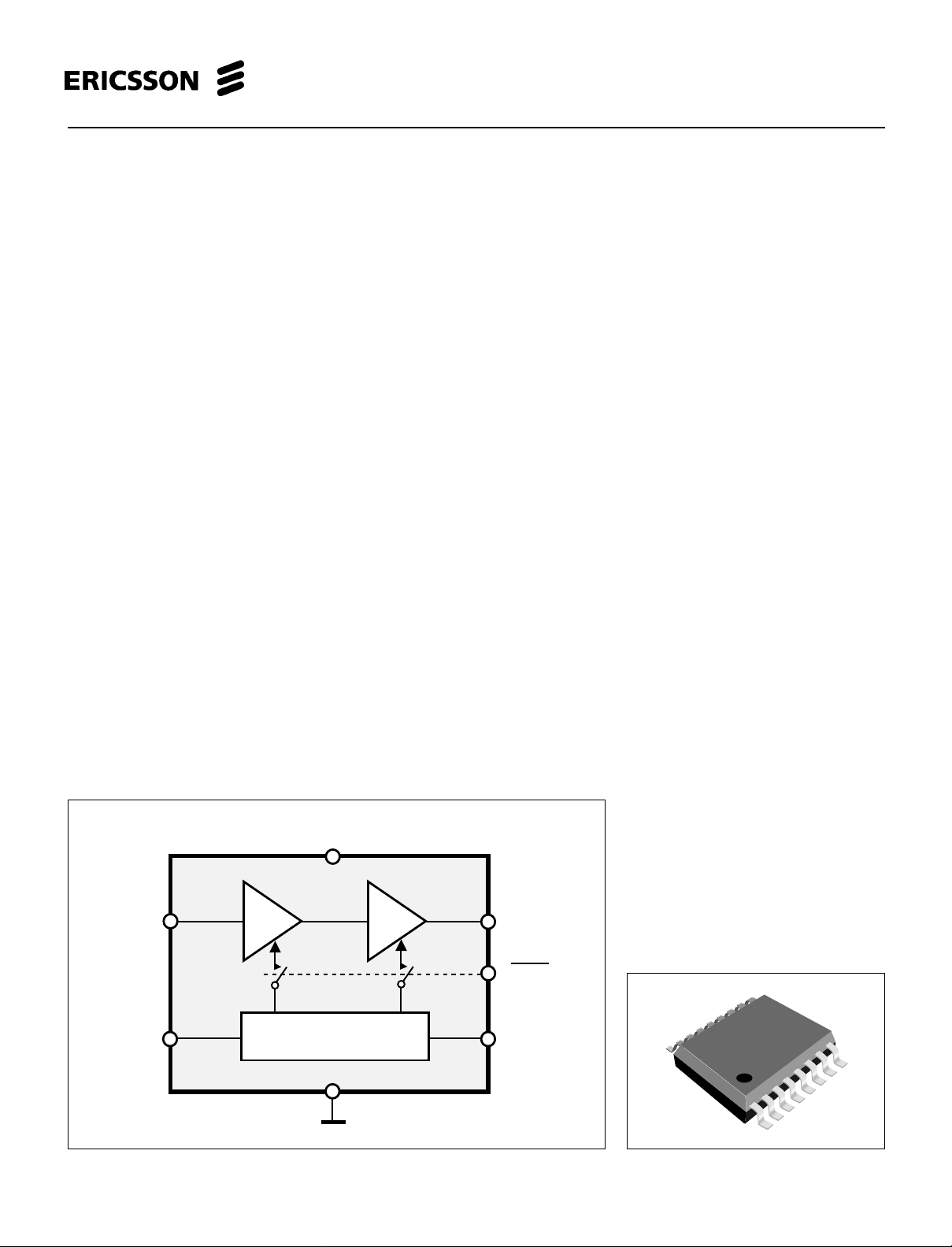
RFin
Power
Control
Figure 1. Block diagram.
BIAS
RFout
B
SEL
TX - ON
Figure 2. Package outlook.
1

PBL 403 10
Maximum Ratings
Parameter Conditions Symbol Min. T yp. Max. Unit
Supply voltage, continuous V
Power control voltage V
Input power P
Operating Case Temperature T
Storage Temperature Range T
CC
APC
IN
OP
STORAGE
DC Electrical Characteristics
VCC = 3.5 V, TA= + 25°C unless otherwise stated.
Parameter Conditions Symbol Min. T yp. Max. Unit
Supply voltage range V
Supply current V
Standby supply current V
Power down leakage current V
Input current, V
APC
= 2.5 V, no RF signal applied I
APC
<=0.5 V , TX-ON=HIGH I
APC
<= 0.5 V , TX-ON=LOW I
APC
0 < V
< 3.5 V 2.0 3.0 mA
APC
CC
CC
STBY
LEAK
-0.5 6.0 V
-0.5 6.0 V
+20 dBm
-40 +85 °C
-30 +100 °C
2.7 5.0 V
150 mA
3.0 mA
5.0 µA
AC Electrical Characteristics
VCC = 3.5 V, f
pulse width = 577 µs, T
Parameter Conditions Symbol Min. T yp. Max. Unit
Frequency range f
Input impedance Z
Input VSWR P
Recommended input power P
Power gain P
Output power P
Power added efficiency η 50 55 %
Output power V
nd
2
harmonic 2 fo tbd dBc
rd
3
harmonic 3 fo tbd dBc
Output Noise RBW=100 kHz, f=925 to 935 MHz tbd dBm
Output Noise RBW=100 kHz, f=925 to 960 MHz tbd dBm
Forward isolation V
Stability, load VSWR All phases, no oscillations. VSWR 6:1
Ruggedness, load VSWR All phases, no damage. VSWR 10:1
Power control for max. P
Power control for min. P
Power control slope -10 dBm < P
= 900 MHz, P
IN
= 8 dBm, V
IN
= +25°C unless otherwise stated. All data measured on evaluation board.
A
OUT
OUT POUT
= 2.5 V, TX-ON = high (VCC), BSEL = low (GND), duty cycle = 12.5 %,
APC
IN
IN
= -10 to +20 dBm VSWR 2:1
IN
IN
= 0 dBm G
IN
= 2.9 V P
CC
< 0.5 V, PIN = -10 to + 10 dBm -25 dB
APC
< -30 dBm V
< 35 dBm tbd tbd dB/V
OUT
P
OUT
OUT
V
APC
APC
880 915 MHz
8.0 12.0 dBm
30 31 dB
34.5 35 dBm
2.5 V
50 Ω
33 dBm
0.5 V
This document contains advance information of a new product. Data given in this document shall be considered as preliminary
and may be changed without notice.
2
 Loading...