


PBL 403 09
Preliminary
August 2000
PBL 403 09
3.6 V Differential Power Amplifier
for DECT Telecommunications system
Description.
The PBL 403 09 is a differential two stage silicon MMIC power amplifier intended for
use in handheld cordless terminals in the 1900 MHz band. It can deliver more than 27
dBm at 1900 MHz into a balanced 50 Ω load using a single 3.6 V supply. The circuit has
a logic input to control transmit on/off and can be operated up to 100 % duty cycle with
minimum performance degradation. The circuit is housed in a specially designed
QSOP16 (150 mil body ) package and the implementation requires only few external
components.
25 GHz ft state-of-the-art deep trench isolated double-poly silicon bipolar process
with additional features for improved wireless performance has been used. On-chip
capacitors and inductors are used for the integrated internal matching network. Special
front-side metallized substrate contacts provide excellent ground paths from active
devices to the highly doped semiconductor substrate and package ground.
V
CC
RF In A
RF Out A & V
CC
Key features.
• 27 dBm output power
• 25 dB small signal gain
• 50 % Power Added Efficiency
• Simple logic on/off power control
• Battery charging conditions to 5.0 V
• ESD protected
• Excellent ruggedness
• On-chip input and interstage
matching
• Differential input matched to 50 Ω
• Easy implementation with a simple
output matching network
• Proven RF Silicon Technology
Reliability
RF In B
Figure 1. Block diagram.
Power Control
PA-ON
RF Out B & V
CC
• Low overall solution cost
Applications.
• DECT
PBL 403 09
Figure 2. Package outlook.
1
PBL 403 09
40
42
44
46
48
50
52
54
22.533.54
Vcc [V]
Pout [dBm]
Pin = 10 dBm
Pin = 4 dBm
Maximum Ratings
Parameter Symbol Min. Max. Unit
Supply voltage, continuous Vcc - 5.2 V
All inputs (zener protection) 6.5 V
Operating case temperature T
Storage temperature range T
op
Stg
Electrical Characteristics at room temperature
Unless otherwise stated the values below are valid for Vcc = 3.6 V, Pin = 4dBm, ZL = 50 Ω and f = 1900 MHz, pulsed mode
t = 417 µs, duty cycle 1/24. All data as measured in the recommended typical application circuit.
Parameter Condition Symbol Min. Typ. Max. Unit
Frequency range f 1880 1930 MHz
Power output PA - ON = low P 27 29 - dBm
Power Added Efficiency P
Power Added Efficiency P
Small signal Gain P
Isolation PA - ON = high, P
and 3
rd
harmonics PA - ON = low, Pin < 4 dBm -35 dBc
nd
2
Input VSWR 1.6:1 3:1
Load Mismatch P
Stability and spurious P
Supply current No input signal present, I
Supply current P
Supply current PA - ON = high I
Rise time P
Fall time P
PA - ON = low -0.5 0.5 V
PA - ON = high Vcc -0.5 Vcc +0.5 V
I ( PA - ON ) low 110 130 µA
in = 10 dBm PAE 45 50 - %
in = 4 dBm PAE 35 43 - %
in = -10 dBm G 25.5 - dB
in = 4 dBm -35 -30 dB
in = 4-10 dBm, Vcc = 5.2 V, no damage for 10 sec.
Load VSWR = 6:1 all phases
in = 4-10 dBm, Vcc = 3.0-5.2 V, All spurious below - 36 dBm
Load VSWR = 5:1 all phases
PA - ON = low
in = 4 dBm IDC 550 mA
out to 1dB from final value. tr 1 µA
Measure time from switch to low.
out to less than -20 dB measured tf 2 µs
from PA - ON pulse switched to high
-25 +80 °C
-30 +100 °C
DC 135 mA
DC 110µA
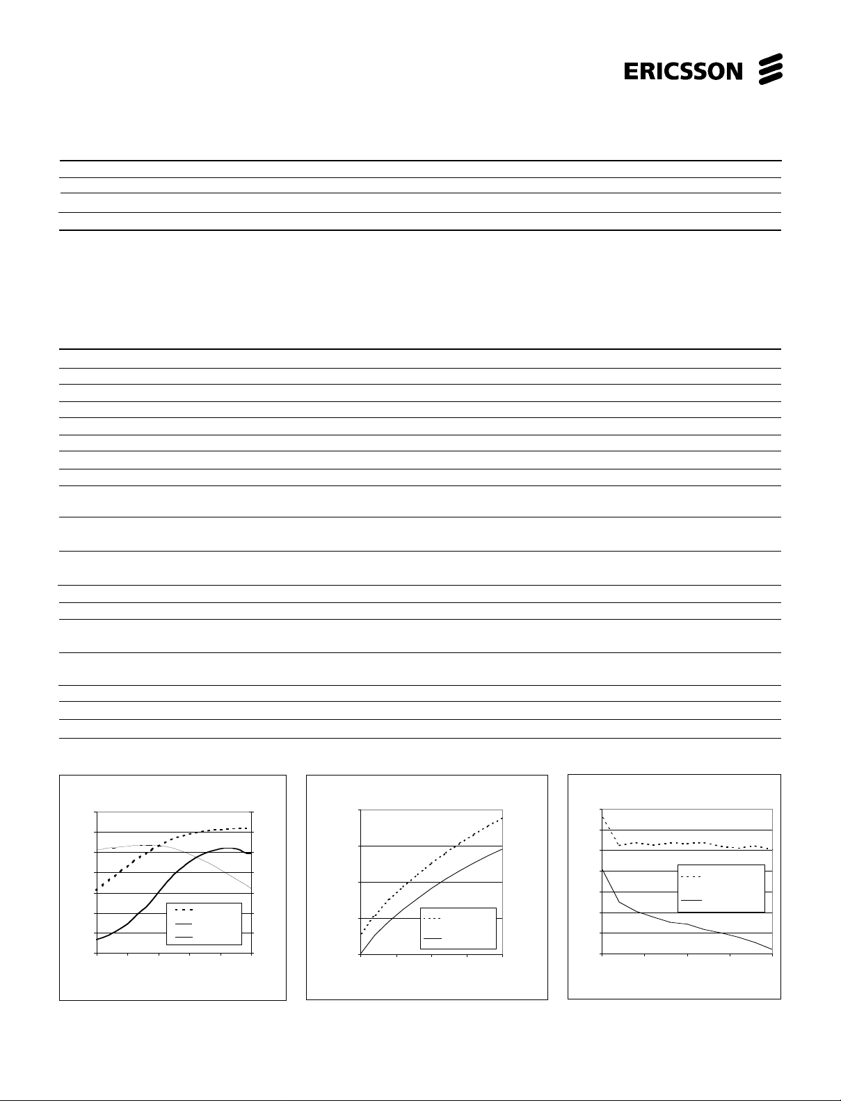
35
30
25
20
15
10
Pout [dBm]or Gain [dB]
5
0
-10 -5 0 5 10 15
Figure 3. P
Pin [dBm]
out
, Gain and PAE vs. P
Vcc = 3.6 V
2
Pout [dBm]
Gain [dB]
PAE [%]
70
60
50
40
30
PAE [%]
20
10
0
in
32
30
28
Pout [dBm]
26
24
2 2.5 3 3.5 4
Figure 4. P
and 10 dBm
Pin = 10 dBm
Pin = 4 dBm
Vcc [V]
out
vs. Vcc for Pin = 4 dBm
Figure 5. PAE vs.Vcc for Pin = 4 dBm
and 10 dBm
 Loading...