

Key Features
• One IC handles GSM900 DCS 1800/
PCS 1900 bands
• High output power: (17 dBm, 13dBm/
13dBm)
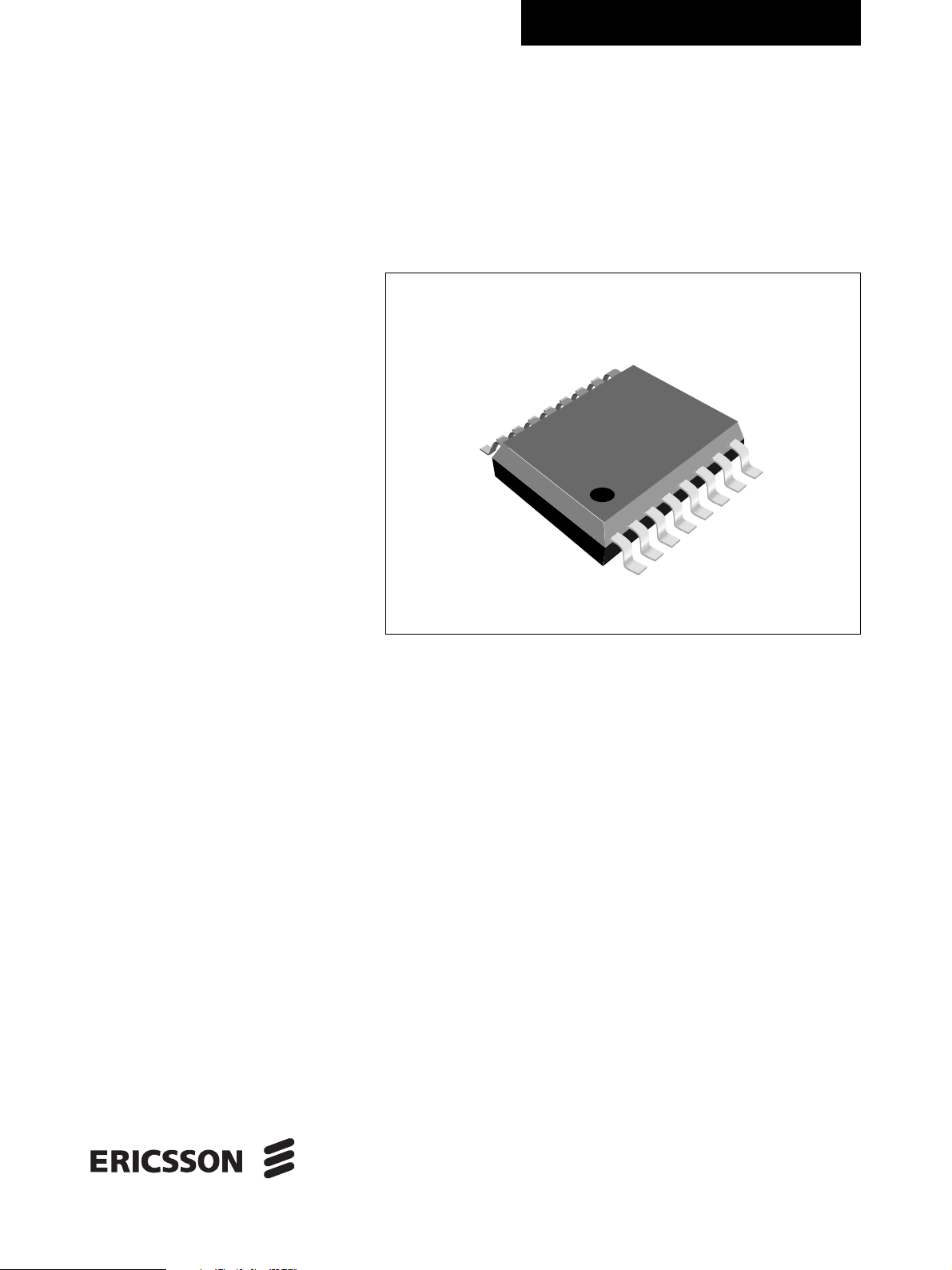
PBL 403 07
GSM Dual Band
Tx_VCO
PBL 40307
16 pin QSOP
Description
The PBL 403 07 is a Dual Band Tx_VCO for use in
GSM dual band terminals.
The resonators for each band are external. The resonator consists of varactor, capacitor and inductor in
series from ground to the VCO resonator pin. The
inductor, capacitor and varactor determines the
oscillation frequency, and also the tuning range.
PBL 403 07
Absolute Maximum Ratings
Parameter Symbol Condition Value Unit
Supply V
Operating case temp. range T
Storage temp. range T
cc
c
stg
5V
-25 to +90 °C
-30 to +100 °C
Electrical Characteristics
Specifications apply measured in a reference fixture.
Parameter Symbol Condition Limits Unit
Min Typ Max
Supply voltage 3.55 3.75 3.95 V
Current Consumption 45 60 mA
Osc frequency OSC_GSM T=25 deg. C nom.
center frequency 880 928 MHz
deviation
Osc frequency OSC_DCS T=25 deg. C nom.
center frequency 1700 1807 MHz
deviation
Osc frequency OSC_PCS T=25 deg. C, 1835 1933 MHz
RF output GSM 15.2 16.7 18.2 dBm
RF output DCS 11.2 12.7 14.2 dBm
RF output PCS 11.2 12.7 14.2 dBm
V
sensitivity GSM V
cont
V
sensitivity DCS/PCS V
cont
Pushing figure Slope for VCC = 3,75 ±0.15V -3 3 MHz/V
Pulling figure VSWR 6:1 All phase F
Spurios, harmonics At TXA, TXB -10 dBc
Phase noise +/-400kHz from carrier -115 dBc/Hz
Output power TXA, TXB Unbalanced or balanced -15 -3 dBm
=0.5-2.5V 28 33 43 MHz/V
cont
=0.5-2.5V 50 60 70 MHz/V
cont
-2 F
c
c
Fc+2 MHz
at PA output
ESD
These devices are ESD sensitive.
2 EN/LZT 146 64 R1A ©Ericsson Microelectronics, February 2001
 Loading...