

PBL 403 05
PBL 40305
January 2001
PBL 403 05
Multiband GSM Power Amplifier
Description.
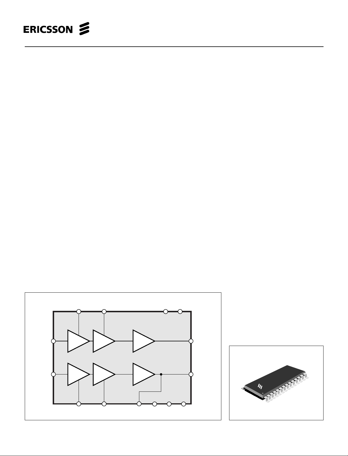
The PBL 403 05 is a dual line-up GaAs MMIC power amplifier intended for use in
multiband GSM terminals. Powered of a 3.2V supply it delivers more than 34.5 dBm
output power at GSM900 and more than 31.5 dBm output power at DCS1800 or
PCS1900 frequencies.
The circuit uses an analog control signal to control the output power level. The circuit
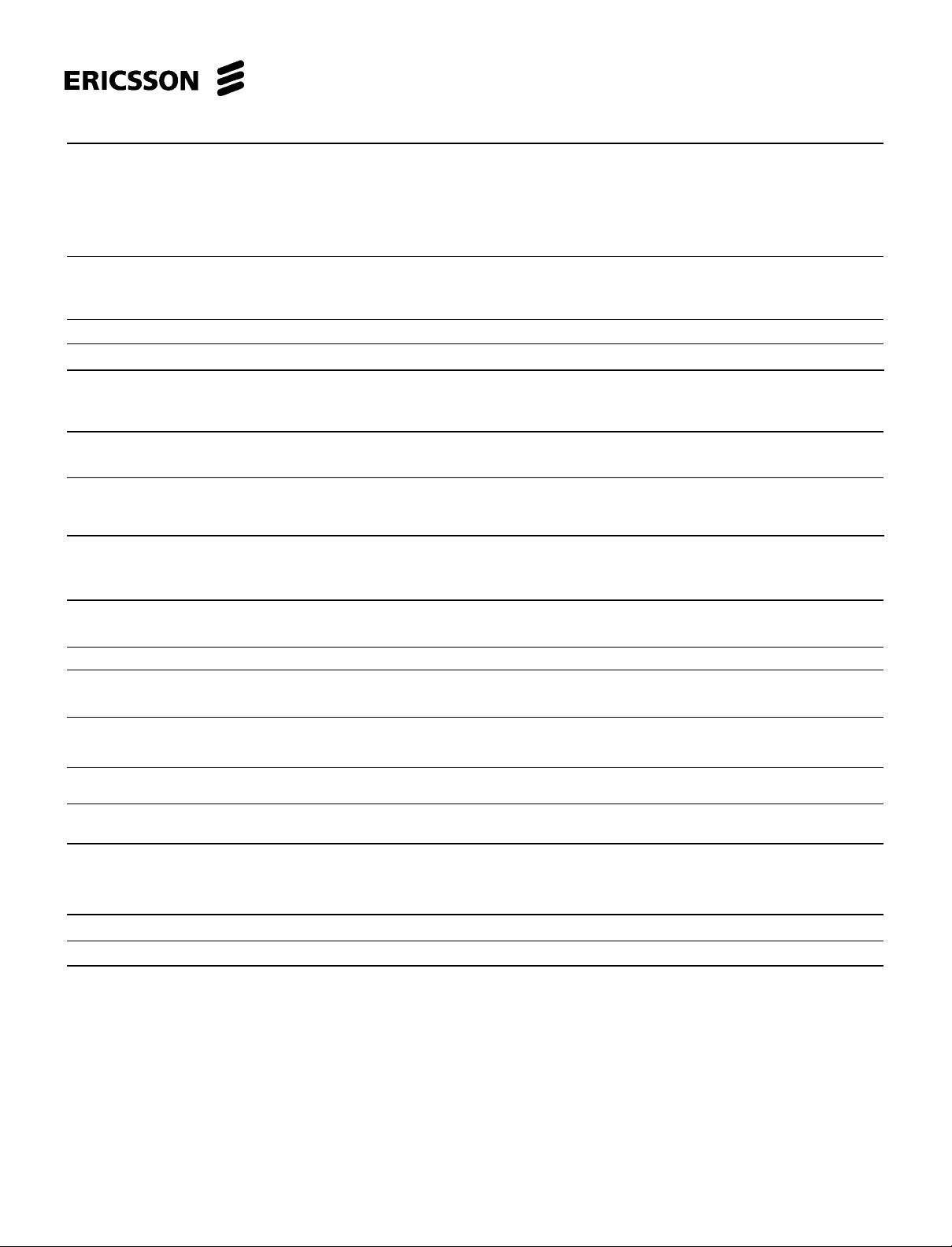
is housed in a specially designed QSOP28 (150 mil body) package with no special
mounting requirements.
The circuit is manufactured in a high performance MESFET process that ensures
ruggednes for environmental variations.
VD1_DCS
VD2_DCS
Current generator
CA
VDC
Key features.
• One IC handles GSM900, DCS
1800 and PCS1900 bands.
• Low cost solution.
• Inputs matched to 50 Ω
• Digital band select function.
• Analog gain control.
• Proven GaAs MESFET-reliability.
• Tape and Reel.
• SMD QSOP 28 package.
RFIN_DCS
RFIN_GSM
VD1_GSM
Figure 1. Block diagram.
VD2_GSM
VD3GSM
VNEG
BIAS
VSEL
VD3_DCS
RFOUTGSM
VAPC
Figure 2. Package outlook.
1

PBL 403 05
Maximum Ratings:
T
= + 25°C unless otherwise stated.
AMB
Parameter Conditions Symbol Min. T yp. Max. Unit
Supply voltage short supply spike V
Supply voltage V
Power control voltage V
Operating Case Temperature T
Storage Temperature Range T
DD
DD
APC
CASE
STORAGE
-25 +80 °C
-30 +100 °C
Electrical Characteristics for PA in GSM 900 mode:
= 3.2 V, T
V
CC
noted. Pulsed operation with pulse width of 577µs and a duty cycle of 1:8. V
Parameter Conditions Symbol Min. Typ. Max. Unit
Output Power V
Power added efficiency P
nd
2
harmonic - 0 dBm < P
rd
3
harmonic - 0 dBm < P
Isolation P
Power degradation P
V
Stability and leakage spurious Output VSWR = 6:1 all phases No parasitic oscillations
Noise power 935 - 960 MHz -90 dBm
Input S11 V
Input S11 P
= + 25°C, Z = 50 Ω, PIN = 10 dBm, f = 880 - 915 MHz and V
AMB
= 3.15 V P
APC
< 34.5 dBm 2 f
OUT
< 34.5 dBm 3 f
OUT
= 11.5 dBm, V
IN
T
= -25 °C to +75 °C
AMB
= 8.5 dBm, V
IN
= 2.8 V, T
APC
<= 0.5 V -30 -20 dBm
APC
= 0.6 V, 33 dBm
SEL
= -25 °C to +75 °C
AMB
All combinations of following when I
parameters: P
V
= 2.7 V to 5.1 V
DD
T
= -25 °C to +75 °C
AMB
925 - 935 MHz
= 0.5 V , -5.2 -5.0 dBm
APC
= 34.5dBm -12 -6.0 dBm
OUT
=5 to 34.5dBm(50Ω) All spurious < -36 dBm
OUT
RBW = 30 kHz
adjusted to give P
APC
= -4.0 V, V
NEG
OUT
AE
o
o
= 34.5 dBm unless othervise
OUT
= 0.0 V.
SEL
34.5 34.7 dBm
50 53 %
-7.0 0 dBm
-27 0 dBm
< 2.2 A
DD
6.0 V
5.0 V
4.2 V
-78 dBm
Electrical Characteristics for PA in DCS 1800 mode:
VCC = 3.2 V, T
dBm unless othervise noted. Pulsed operation with pulse width of 577µs and a duty cycle of 1:8. V
Parameter Conditions Symbol Min. Typ. Max. Unit
Output Power V
Power added efficiency P
nd
2
harmonic - 0 dBm < P
rd
3
harmonic - 0 dBm < P
Isolation PIN = 10.5 dBm, V
Power degradation P
V
2
= + 25°C, Z = 50 Ω, PIN = 9 dBm, f = 1710 - 1785 MHz / 1850 - 1910 MHz and V
AMB
= 3.15 V P
APC
= 31.5 dBm P
OUT
< 31.5 dBm 2 f
OUT
< 31.5 dBm 3 f
OUT
= 0.5 V -35 -30 dBm
T
= -25 °C to +75 °C
AMB
= 7.5 dBm, V
IN
= 2.8 V, T
APC
APC
= 2.85 V 30 30.5 dBm
DD
= -25 °C to +75 °C
AMB
OUT
AE
o
o
adjusted to give P
APC
= -4.0 V, V
NEG
SEL
OUT
= 2.0 V.
= 31.5
31.5 31.7 dBm
37 41 %
-8.0 0 dBm
-15 0 dBm
PBL 403 05
Parameter Conditions Symbol Min. T yp. Max. Unit
Stability and leakage spurious Output VSWR = 6:1 all phases No parasitic oscillations
All combinations of following when I
parameters: P
V
= 2.7 V to 5.1 V RBW = 3 MHz
DD
T
= -25 °C to +75 °C
AMB
Noise power 1805 - 1880 MHz -76 dBm
935 - 960 MHz
=5 to 31.5dBm(50Ω) All spurious < -36 dBm
OUT
RBW = 30 kHz
925 - 935 MHz -70
Input S11 V
Input S11 P
= 0.5 V, -5.0 -4.0 dBm
APC
= 31.5dBm -14 -6.0 dBm
OUT
Common specifications:
Parameter Conditions Symbol Min. Typ. Max. Unit
Isolation at GSM RF output f = f
when DCS is active f = 2 • f
0
, f0 = 1750 - 1785 MHz -30 dBm
0
< 2.20 A
DD
-82 dBm
-20 dBm
Isolation at DCS RF output f = 2 • f
when GSM is active f = 3 • f
0
, f0 = 880 - 915 MHz -30 -25 dBm
0
-18 -15 dBm
Power regulation characteristics:
Parameter Conditions Symbol Min. Typ. Max. Unit
Power control range GSM: V
DCS: V
Power control slope V
APC
Switching time Step in V
= 0.5 - 3.15 V -20 34.5 dBm
APC
= 0.5 - 3.15 V -30 31.5 dBm
APC
= 0.5 - 3.15 V 150 dB/V
giving P
ref
= -15 to 2 µs
OUT
32.5 dBm, up and down
Power control current V
consumption
Band select current consumption V
Negative supply current V
<= 3.15 V I
APC
V
= 0 - 3 V
SEL
= 0 - 3 V, V
SEL
= 0 V, V
SEL
<= 3.15 V I
APC
<= 3.15 V I
APC
APC
SEL
NEG
45mA
0.01 0.1 mA
5.5 7.0 mA
consumption
Current generator:
Parameter Conditions Symbol Min. Typ. Max. Unit
Input resistance VDC- VCA < 0.8 V R
Charge current V
= 1.5 - 5.0 V, VCA = 0 V I
DC
ON
GSAT
100 150 Ω
6.7 10 mA
3
 Loading...