

Preliminary
January 2001
PBL 402 15
PBL 402 15
RF Transceiver circuit for the Digital
Enhanced Cordless Telecommunications
(DECT) system
Description.
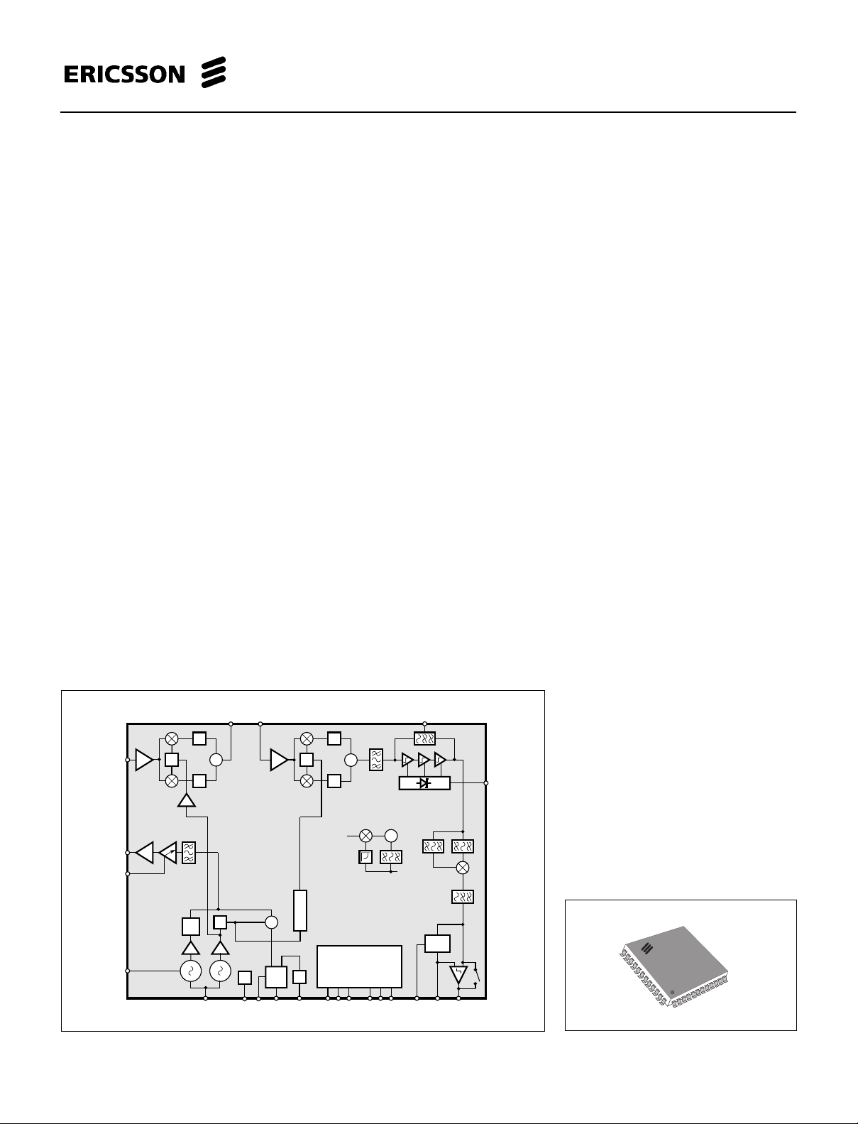
The PBL 402 15 is a complete RF transceiver to be used in the Digital Enhanced
Cordless Telecommunications ( DECT ) system. It is designed to interface to various
base-band controllers.
The circuit contains transmit and receive functions that share integrated high stability
VCO´s and a phase locked loop function ( PLL ). All functionality is controlled through a
3-wire bus interface with optional hard wire lines.
The receive section comprises of a low noise image reject down conversion to the
first intermediate frequency, an external channel filter, a second down convertion to a
second intermediate frequency, an integrated channel pass filter, a high gain limiting
amplifier, a received signal strenght indicator with DC compensation loop, a self aligned
frequency discriminator and a preamble based data slicer.
The transmit section comprises of a signal gate and a pre-power amplifier. Data
transmission is achieved by direct open loop modulation of the Tx VCO.
Key features.
• High Tx output power to +7dBm
• Integrated PLL and high stability
VCO´s
• 3-line serial interface bus
• Minimum 2.7 V supply voltage
• Low current consumption
• Differential Rx input and Tx output
• Flexible interface to various base band controllers
• Exellent performance with Ericsson´s
power amplifier PBL403 09
• Low cost
Applications:
• DECT Handset and base station
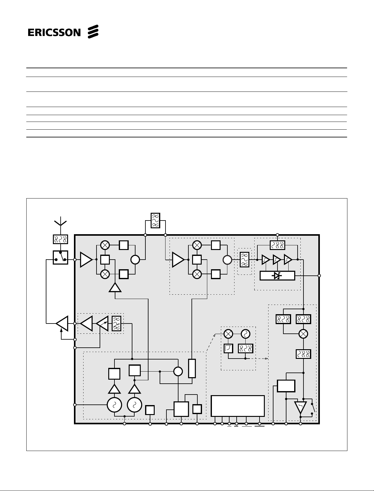
Figure 1. Block diagram.
• Wireless local area network ( WLAN )
• Wireless local loop ( WLL )
PBL 402 15
Figure 2. Package outlook.
1
PBL 402 15
C0
6.8nF
R0
3.9k
Regulated supply
Vcc
VccVCO
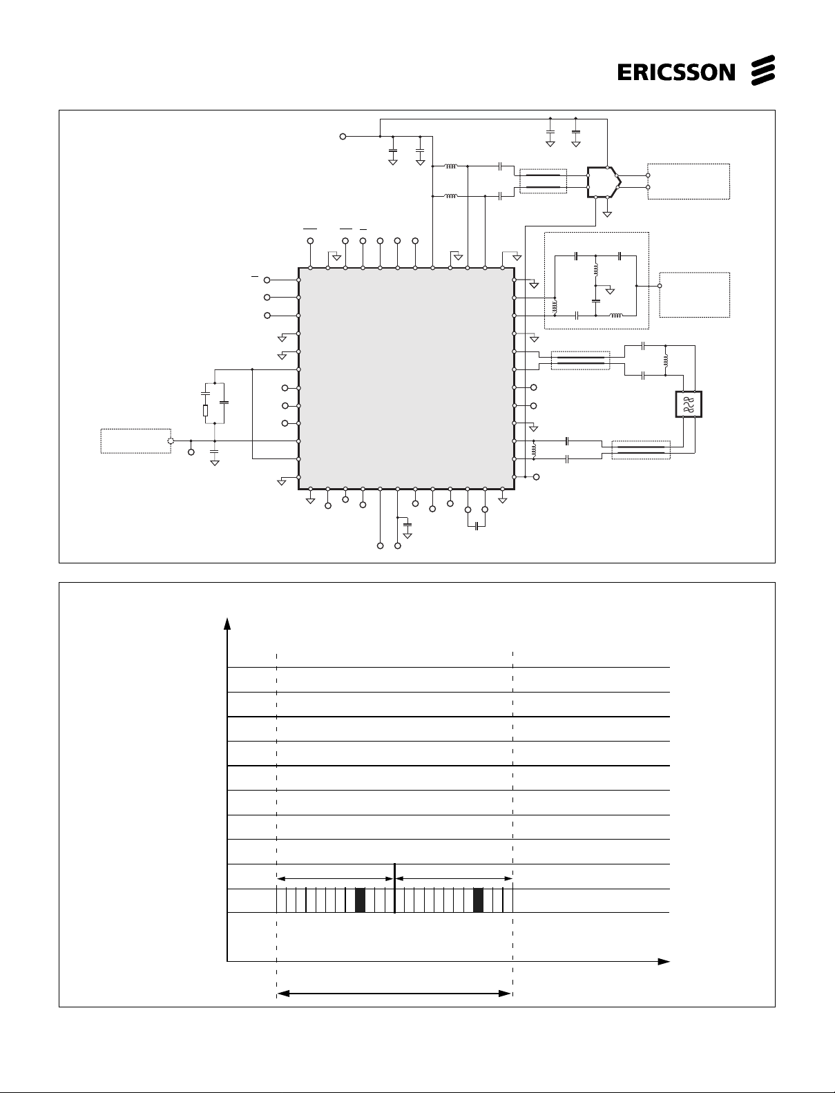
Figure 3. DECT application.
C2
100nF
C1
680 pF
VccPLL
EN
REF
GND
CP
VccCP
NC
NC
V
TUNE
1
3
4
5
10
11
12
GND
PA - Vcc
RxEN TxEN
GND GND
48
47
2
6
7
8
9
14
13
DTx
C14
C15
2.2nF
8pF
GND
ST CK D
46 45 44 43 42 41 40 39 38 37
GATE
PBL402 15
15 16 17 18
MOD
SHold
19
VccFM
C3
2nF
DSL
DRx
L5
4.7nH
L6 4.7nH
20
21 22 23 24
Vcc
RSSI
C18 22nF
C16
10nF
C12 1pF
C13 1pF
MS lines 3
GND
36
GND
35
34
33
32
31
30
VccIF
29
28
27
L1
140nH *
26
25
GND
* These components for matching are not needed if Murata filter is used
C17
33pF
Vcc
+in
+out
-in
-out
Gate
Can also be a balun type of solution
GND
LD
GND
PA Gate
C10 8pF
L4
8.2nH
C11 8pF
MS lines 1
C6 68pF *
C7 68pF *
C8 1pF
L3
5.6nH
1pF
C9
L2
5.6nF
C4 11pF *
C5 11pF *
IF - SAW filter
MS lines 2
Consult PBL40309 for PA
output matching requirements
RF in to Rx
Feed from antenna switch.
( 50 ohms )
L0
180nH *
in
_
+
_
+
out
10 channels
Channel spacing
1.728 MHz
Channel 0
Frequency
9
8
7
6
5
4
3
2
1
EUROPEAN DECT Band 1880 - 1900 MHz
TDMA ( time division multiple access )
Frequency and time division.
Base to Mobile Mobile to Base
123456789101112 13 14 15 16 17 18 19 20 22 2321
0
24 time slots
1 slot = 416.67µs
Frame =10 ms
A-word
CNT_A
1
2
3
4
5
6
7
8
9
10
each slot contains, a synchronisation field,
control info, data package and error control.
Frequency MHz
1881.792
1883.520
1885.248
1886.976
1888.704
1890.432
1892.160
1893.888
1895.616
1897.344
Time
Figure 4. The European DECT band .
2

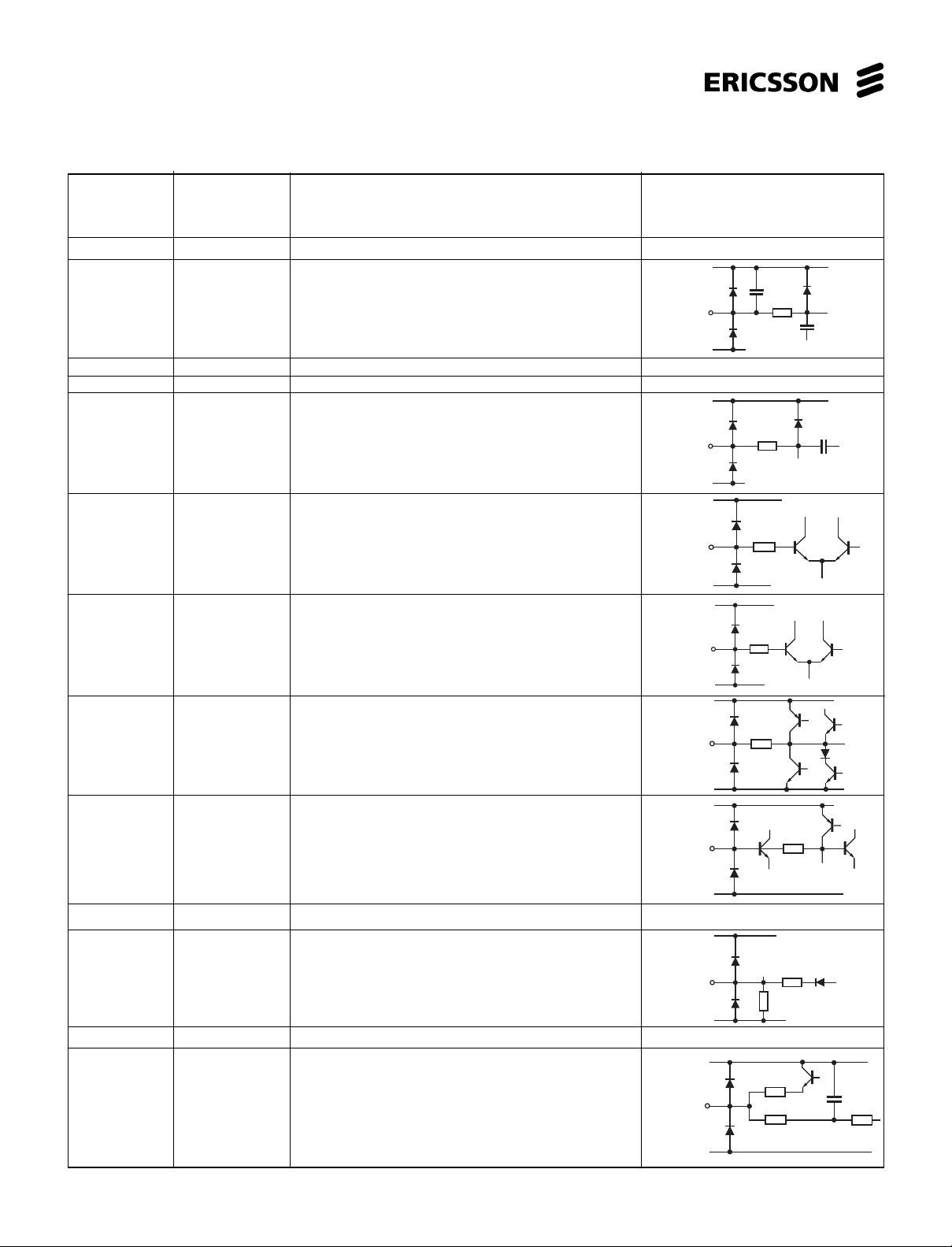
RXEN
VCCPLL
EN
GndPLL
165 k
VCCPLL
REF
GndPLL
DIE
TXENSTCKDGATE
VccRF
GndRF
TX+
TX-
PBL 402 15
GndRF
48 47 46 45 44 43 42 41 40
1
EN GndRF
CP
NC
NC
2
3
4
5
6
7
8
9
10
11
12
13
14
GndFM
1516171819 20
MOD
DRX
SHOLD
DSL
DTX
RSSI
VccFM
REF
VccPLL
GndPLL
GndCP
VccCP
VccVCO
VTUNE
GndVCO
39 38
21 22 23 24
CAP-
CAP+
VccRSSI
37
36
35
34
33
32
31
30
29
28
27
26
25
GndRSSI
RX+
RXGndRF
IFOUT+
IFOUT-
LD
VccIF
GndIF
IFIN+
IFINPA Gate
Figure 5. Pinning configuration.
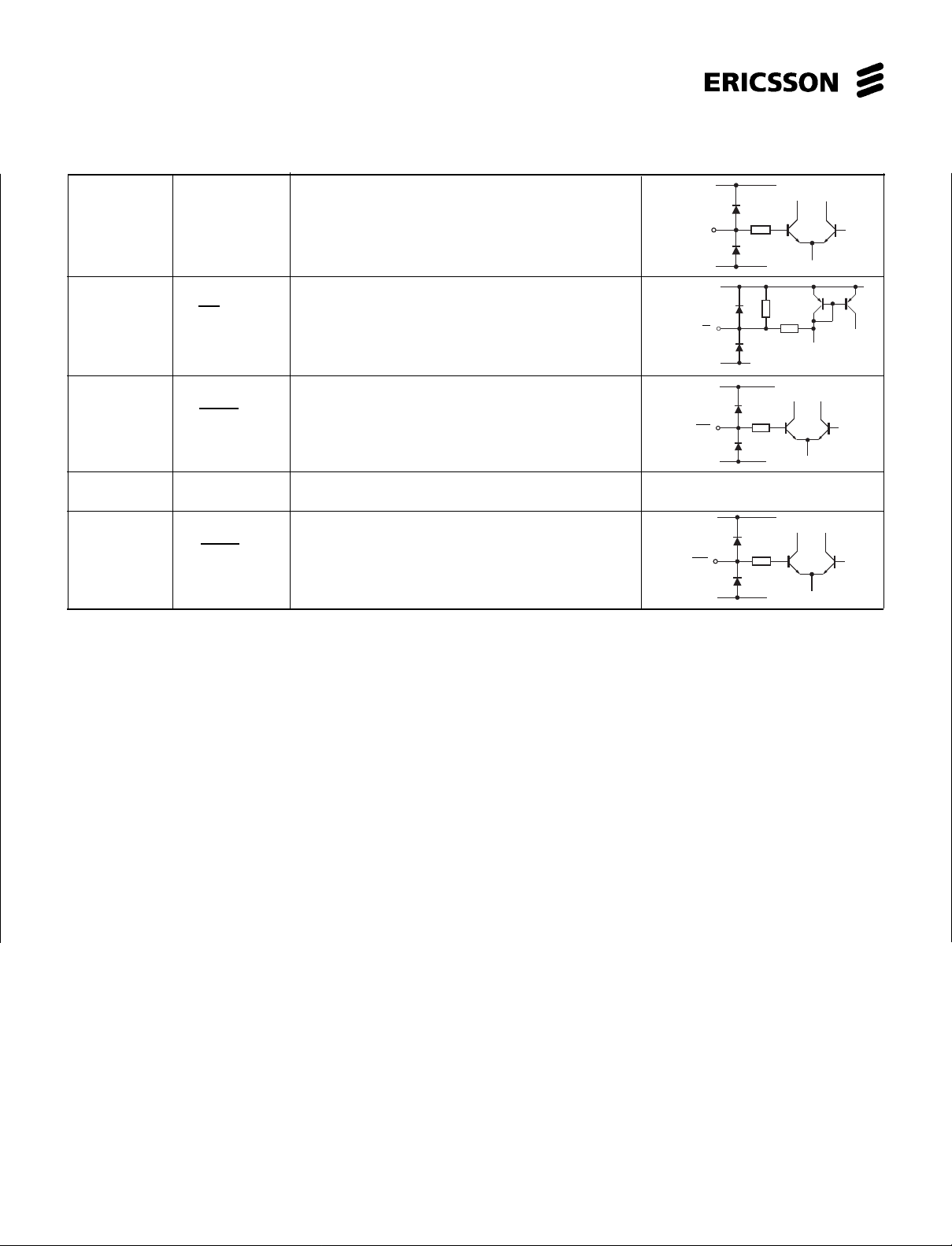
Pin Descriptions:
Refer to pin configuration.
Pin number Name Function Schematic in/output of the pin
1 EN Enable 3-wire interface and synthesiser.
2 REF PLL reference clock input
3VCCPLL Voltage supply to the frequency synthesiser.
4 GndPLL Ground connection to the frequency synthesiser.
5 GndCP Ground connection to the charge pump.
6 CP Charge pump output.
7VCCCP Voltage supply to the charge pump.
Clamp to GndPLL
A diode to GndCP and GndRF
A diode to GndPLL and GndVCO
VCCCP
CP
GndCP
Clamp to GndCP
3
PBL 402 15
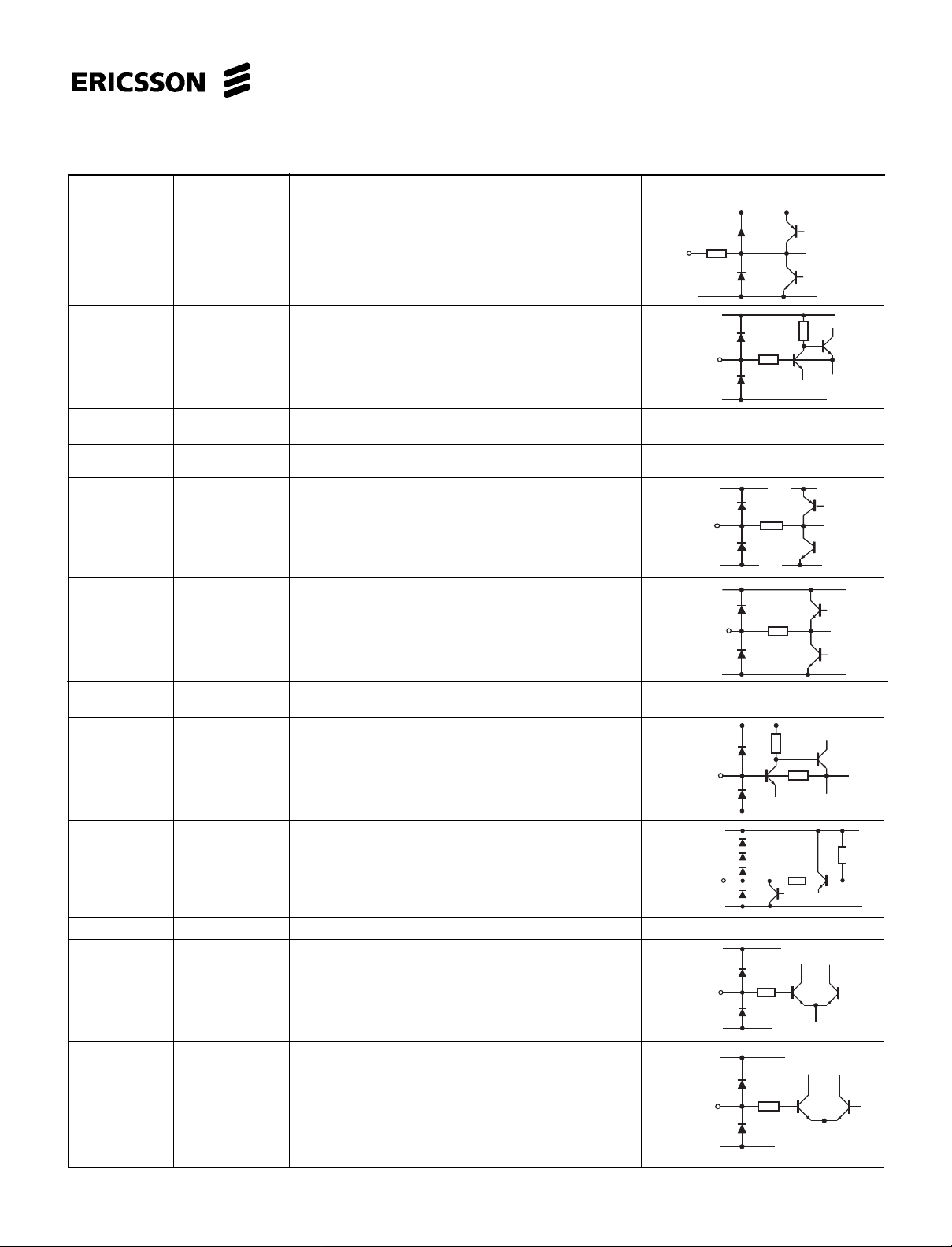
Pin Descriptions (cont.):
Pin number Name Function Schematic in/output of the pin
8 Not connected
9 Not connected
10 VCCVCO Voltage supply to the VCO
11 VTUNE Tuning voltage input for the VCO
12 GndVCO Ground connection to the VCO
13 GndFM Ground connection to the FM discriminator section.
14 DTX Tx data input for either analog or logic signal.
15 MOD Apply modulation. The PLL is set into open loop
condition and modulation is applied to the VCO.
16 SHOLD Slice level hold logic input. (In Tx mode this input
may also act as the MOD pin).
N/C
Clamp to GndVCO
VCCVCO
VTUNE
GndVCO
A diode to GndCP and GndFM
VCCFM
DTX
GndFM
VCCFM
MOD
GndFM
VCCFM
SHOLD
GndFM
VCCFM
Bias
Bias
17 DRX Rx data output of FM discriminator for either analog
or logic signal.(In standby mode outputs lock detect)
18 DSL Data slice level output.
19 VCCFM Voltage supply to the FM discriminator section.
20 RSSI RSSI output of limiting strip detector chain.
21 VCCRSSI Voltage supply to the RSSI section.
22 CAP+ External stabilising capacitors for limiting strip
DC input offset correction loop.
23 CAP-
DRX
GndFM
VCCFM
DSL
GndFM
Clamp to GndFM
VCCRSSI
RSSI
GndRSSI
Clamp to GndRSSI
VCCRSSI
CAP+/CAPBoth inputs alike
GndRSSI
4
PBL 402 15
VCCRF
TX-/TX+
Both inputs alike
GndRF
VCCPLL
GATE
GndPLL
Bias
Pin Descriptions (cont.):
Pin number Name Function Schematic in/output of the pin
24 GndRSSI Ground connection to the RSSI.
A diode to GndFM and GndIF
VCCRF
25 PA Gate Output control signal for external PA power on/off.
26 IFIN- Rx IF inputs to internal channel filtering, limiting
amplifiers,RSSI and FM discriminator. Internally
27 IFIN+ matched to 300 Ω.
28 GndIF Ground connection to the down IF convertor and
channel filter sections.
29 V
CCIF Voltage supply to the down IF convertor and
channel filter sections.
30 LD Lock detect.
31 IFOUT- Rx IF outputs to external adjacent channel filter.
Internally matched to 300Ω.
32 IFOUT+
33, 36 GndRF Ground connection to the RF sections.
37, 40
PA - Gate
GndRF
VCCIF
IFIN-/IFIN+
both inputs alike
GndIF
A diode to GndFM and GndIF
Clamp to GndIF
VCCRF
LD
GndRF
VCCRF
IFOUT-/IFOUT+
both outputs alike
GndRF
A diode to GndIF and GndPLL
VCCRF
34 RX- RF inputs to LNA and image reject mixer.
35 RX+ Internally matched to 100Ω.
38 TX- Tx outputs to external PA. Internally matched to
39 TX+ 100 Ω. Each output requires an externalchoke
to VCC.
41 VCCRF Voltage supply to the RF sections.
42 GATE Input to gate the Tx output power.
43 D Serial interface, Data .
RX-/RX+
both inputs alike
GndRF
Clamp to GndRF
VCCPLL
D
GndPLL
Bias
5
PBL 402 15
VCCPLL
ST
GndPLL
165 k
Pin Descriptions (cont.):
Pin number Name Function Schematic in/output of the pin
VCCPLL
44 CK Serial interface, Clock .
45 ST Serial interface, Strobe .
46 TXEN Transmitter enable.
47 DIE Gnd. pin used for internal shielding. Connected
to DIE substrate.
48 RXEN Receiver enable
CK
GndPLL
VCCPLL
TXEN
GndPLL
VCCPLL
RXEN
GndPLL
Bias
Bias
Bias
6
PBL 402 15
Maximum Ratings
Parameter Condition Symbol Min. Typ. Max. Unit
Supply voltage Vcc 5.5 V
Voltage applied between two different Vccdiff 0.6 V
supply pins, except VccRF
Voltage applied between two Grounds are clamped together Gnddiff 0.6 V
different ground pins
Maximum input power LNA input P
Maximum power dissipation P
IC storage temperature T
Lead temperature solder, 10 sec. T
(a). Under continous operation and during power-up sequences.
Handling
Every pin withstands the ESD test in accordance with MIL-STD-883 (method 3050) and IEC 68-2.
(a)
(a)
by diodes
max 10 dBm
D 250 mW
S -65 150 °C
LEAD 300 °C
PIN switch
PA-GATE
RXIN
TXOUT
GATE
DTX
IR RX
Modulator
TX
CAP
RSSI
RSSI
FM Demod
Slice
control
PLL
IFIN
IR IF
π/4
÷2
IF2
+
ƒ-φ
÷R
-π/4
+
IF Filt
Slave PLL
Control
IFOUT
π/4
π/4
-π/4
-π/4
+
÷2
LD
÷2
÷2
×2
Figure 6. Block diagram.
VTUNE
LD
MOD
CP
REF
D
CK
RXEN
EN
ST
TXEN
SHOLD
DSL
DRX
7
 Loading...