

Ericsson PBL38814-1SO, PBL38814-1SOT, PBL38814-1N Datasheet
May 1998
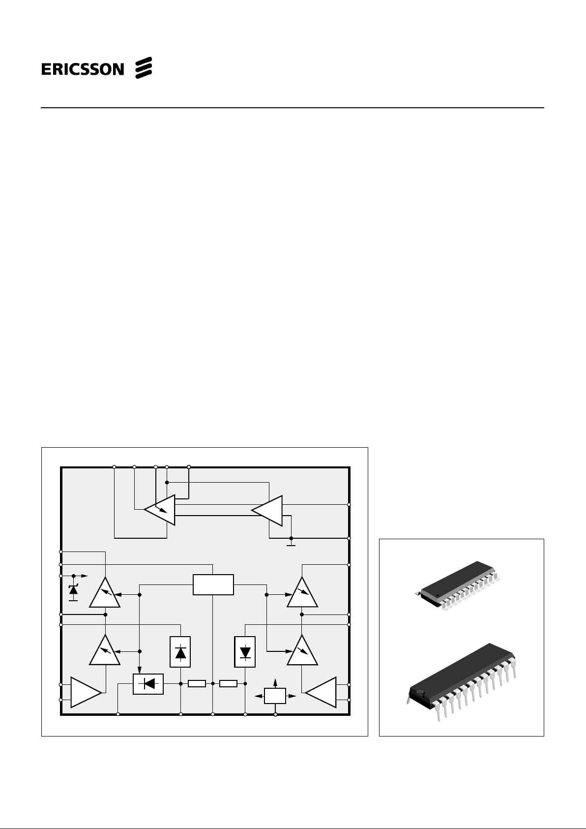
Figure 1. Block diagram.
24 pin DIP
PBL 388 14
Voice - switched 2-channel Circuit with
loudspeaker amplifier
24 pin SO
Description.
1
The PBL 388 14 contains all the necessary circuitry, amplifiers, detectors,
comparator and control functions to implement a high performance voice switched
handsfree two- way communication system. The gain dynamics (attenuation between
channels) is selectable (25dB or 50dB) via a separate pin. A background noise
detector in the transmitting channel reduces the influence of continuous external noise
signals to the switching .
The PBL 388 14 is designed for mains powered handsfree telephones, vehicular
mobile telephone handsfree systems and handsfree intercom systems. Automatic
volume attenuation in the power amplifier extends the operating range at low supply
currents. The circuit has two special features, the power amplifiers volume control can
be implemented either as an ac. potentiometer control or as a digital control by a µprocessor (dc. control) and that the feedback loop of the power amplifier is accessible
thus making it possible to add a simple external power stage driving low impedance
loudspeakers up to several watts.
Filtering is possible of both, the audio and the speech switching control signals,
in both transmitter and receiver channels.
Key Features
• Minimum of external components
needed for function.
• Selectable gain dynamics. (25 or 50
dB)
• Low power consumption: ≈1mA at 3.3V
(typical) for speech switching, audio
power amplifier quiscent current ≈1mA.
• Drives an 25 - 50 ohm loudspeaker
without a transformer.
• Background noise compensation in the
transmitting channel with hold function
at receive.
• Input amplifiers of both channels have
balanced inputs.
• Exellent noise performance.
• Encapsulated in 24 pin plastic ”skinny”
DIP and 24 pin SO .
F2
F3
F6
F5
F1
PBL 388 14
F4
3
1
2
8
9
10
14
15
12
23
17
18
19
22
24
4
+
+
–
–
+
21
11
13
Ref.
5
16
Control
6
7
20
PBL 388 14
PBL 388 14
PRELIMINARY
2
PBL 388 14
Maximum Ratings
Parameter Symbol Min Max Unit
Speech switch supply current I
D
10 mA
Speaker amplifier supply current I
+L
130 mA
Voltage pin 1-14 -0,5 Vpin
15
+0.5 V
Operating temperature T
Amb
-20 +70 °C
Storage temperature T
Stg
-55 +125 °C
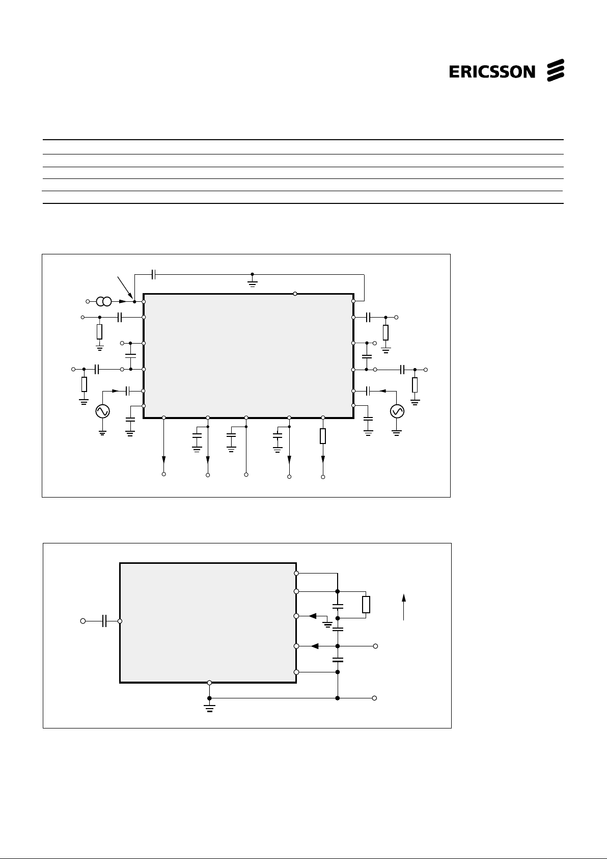
Figure 2. T est circuit. Reference figure No. 2.
Figure 3. T est circuit. Reference figure No. 3.
+
LSP 19
22
18
+
100
16 V
µ
F
µ
0.015
used only
with inductive load
I
+L
GND
17
V
in
Input
23 LSP
in
50Ω
Load
PBL 388 14
1 µF
0.015µ
VOL 21
V
out
V
A
+
-
I
VOL
LL 20
V
A
GND
A
15
V
Txout
CTR
V
V
CMP
V
TxDet
V
Rxout
+
10 µF
CMP CTR
GND
24
17
8
Det
N
Tx
Detout
4
Tx
out
Rx
Detout
in
-Rx
2
1 µF
Rxin
I
V
Rxin
+
NDet
R
CTR
C
TxDet
I
TxDet
0,1µF
C
RxDet
V
RxDet
I
CTR
V
NDet
RxDet
I
PBL 388 14
12
Rx
out
R
Rxout
10 µF
+
1
3
5
F2
out
14
1 µF
Txout
R
100µF/16V
V+16
+
V
+
D
I
I
Txin
V
Txin
4.7 µF
+
+
+
+
+
Tx
Detin
-Tx
in
+Tx
in
in
+Rx
11
Rx
Detin
13F5out
10 µF
+
F5
out
R
F5
out
C
Rx
1 µF
+
10 µF
+
F2
out
R
F2
out
C
Tx
6
9
10
7
Ref.

3
PBL 388 14
Electrical Characteristics
f = 1 kHz, T = 25°C, R
CTR
=0, C
TxDet
= 0, R
Txout
= ∞, R
Rxout
= ∞, R
F2out
= ∞, R
F5out
= ∞, CTx= 0, CRx= 0, C
RxDet
= 0 and
I
D
=1.0mA unless otherwise noted.
Ref.
Parameter fig. Condition Min. Typ. Max. Unit.
Speech control section
T erminal voltage, V
+
2I
D
= 1.0mA 3.3 V
Internal reference voltage, V
Ref
2 1.96 V
Frequency response for all amplifiers 2 200 - 3400 Hz, Relative 1 kHz -1 1 dB
Transmit gain, 20 •
10
log(V
Txout
/V
Txin
)2V
CMP
= V
Ref
- 0.1 V 40.5 43 dB
V
CMP
= V
Ref
+ 0.1 V -7 -4.5 dB
V
CMP
= V
Ref
- 0.1 V R
CTR
=100k, V
CTR
=V+ 40.5 43 dB
V
CMP
= V
Ref
+ 0.1 V R
CTR
=100k, V
CTR
=V+ 18 20.5 dB
Receive gain, 20 •
10
log(V
Rxout
/V
Rxin
)2V
CMP
= V
Ref
+ 0.1 V 26.5 29 dB
V
CMP
= V
Ref
- 0.1 V -21 -18.5 dB
V
CMP
= V
Ref
+ 0.1 V R
CTR
=100k, V
CTR
=V+ 26.5 29 dB
V
CMP
= V
Ref
- 0.1 V R
CTR
=100k, V
CTR
=V+ 4 6.5 dB
Max transmit detector gain, 2 V
TxDet
< 200 mVp , CRx = 100nF
20 •
10
log(V
Txdet
/V
Txin
)V
CMP
= V
Ref
- 0.1 V 67 dB
V
CMP
= V
Ref
+ 0.1 V 36.5 42 dB
Max receive detector gain, 2 V
RxDet
< 200 mVp , CTx = 100nF
20 •
10
log(V
Rxdet
/V
Rxin
)V
CMP
= V
Ref
+0.1 V 53 dB
V
CMP
= V
Ref
- 0.1 V 22.5 28 dB
Background noise rectifier gain, (note 1) 2 V
CMP
= V
Ref
- 0.1 V , C
Txdet
=1µF 6.0 dB
V
CMP
= V
Ref
+ 0.1 V, C
Txdet
=1µF Hold
+ TxIn input impedance 2 80 100 120 kΩ
- Tx
In
input impedance 2 2.4 3.0 3.6 kΩ
+ Rx
In
input impedance 2 120 140 160 kΩ
- Rx
In
input impedance 2 16 20 24 kΩ
Tx
Out
ac, load impedance 2 10 kΩ
Rx
Out
ac, load impedance 2 10 kΩ
F2
Out
ac, load impedance 2 10 kΩ
F5
Out
ac, load impedance 2 10 kΩ
Transmitter channel output swing, v
TxOut
2 2% distortion,R
Txout=RRxout
=10k Ω 500 mV
p
Receiver channel output swing, v
RxOut
2 2% distortion,R
Txout=RRxout
=10k Ω 500 mV
p
Transmitter output noise, v
TxOut
2 V
CMP
= V
Ref
- 0.1 V , v
TxIn
= 0 V -75 dB
psof
Receiver output noise, v
RxOut
2V
CMP
= V
Ref
+ 0.1 V , v
RxIn
= 0 V -80 dB
A
Tx
Det
sink current, I
TxDetOut
2V
TxDetIn
= V
Ref
+ 0.1 V -6.0 -2.5 mA
Rx
Det
source current, I
RxDetOut
2V
RxIn
= V
Ref
- 0.1 V 2.5 6.0 mA
Tx
Det
source current, I
TxDet
2V
CMP
= V
Ref
- 0.1 V 30 µA
Rx
Det
sink current, I
RxDetOut
2V
RxDetIn
= V
Ref
+ 0.1 V -30 µA
Tx
Det
swing relative to V
Ref
, V
TxDetOut
2V
TxDetIn
= V
Ref
+ 0.1 V (note 2) -0.7 V
Rx
Det
swing relative to V
Ref
, V
RxDetOut
2V
RxDetIn
= V
Ref
- 0.1 V (note 2) +0.7 V
N
Det
sink current (fast charge), I
NDet
2V
TxDetIn
= V
Ref
- 0.1 V -3 -1 mA
V
CMP
= V
Ref
- 0.1 V
N
Det
source current, I
NDet
2V
TxDetIn
= V
Ref
+ 0.1 V 3 5 7 µA
V
CMP
= V
Ref
- 0.1 V

4
PBL 388 14
Ref.
Parameter fig. Conditions Min. Typ. Max. Unit.
N
Det
leakage current (hold), I
NDet
2V
TxDetIn
= V
Ref
- 0.1 V , -100 nA
V
CMP
= V
Ref
+ 0.1 V ,
N
Det
swing relative to V
Ref
, V
NDet
2V
TxDetIn
= V
Ref
+ 0.1 V , 0.45 V
V
CMP
= V
Ref
- 0.1 V
CMP (comparator) sensitivity, 2 Tx mode = max Tx gain, 40 80 mV
transmit (Tx) mode to receive 12 Rx mode = max Rx gain
(Rx) mode or vice versa
CTR voltage for 25 dB dynamics, V
CTR
2,14 R
CTR
=100kΩ V
+
V
CTR voltage for mute, V
CTR
2,14 1.1 1.6 V
CTR voltage for disable, V
CTR
2,14 0.9 V
Loudspeaker amplifier
Operating voltage, V
A
3 2.5 12 V
Current consumption (no signal), I
+L
3VA = 3.0 V 1 2.3 mA
3V
A
= 5.0 V 2 mA
3V
A
= 12.0 V 4 9 mA
Current consumption 3 V
A
= 3.0 V 7 mA
(output swing at 5% dist.) 3 V
A
= 5.0 V 13 mA
3V
A
= 12.0 V 30 mA
Swing at 5% dist., V
Out
3VA = 3.0 V 0.6 0.85 V
p
3VA = 5.0 V 1.5 1.7 V
p
3VA =12.0 V 3.6 4.0 V
p
Gain 3 VA =5.0 V , I
VOL
= 0 34.5 36.5 38.5 dB
Frequency response 3 200 to 3400 Hz, relative 1kHz, -1 1 dB
Amplifier power efficiency (5% dist), n 3 V
A
= 3.0 to 12.0 V ,
n = 100 • P
Load/PSupply
40 %
Input impedance pin 23 3 24 30 36 kΩ
Notes
V
NDet
- V
Ref
1. 20 •
10
log ( )
V
TxDet
- V
TxDetO
V
NDet
= voltage at noise detector output
V
Ref
= reference voltage (about 2 V) see figure 2.
V
TxDet
= Voltage at transmit detector output.
V
TxDetO
= voltage at transmit detector output at the point
when the voltage at the noise detector starts
moving when a signal at transmit channel input is
gradually increased (threshold, typical value 30 mV)
2. Depends on V
+
. Channels are tracking.

5
PBL 388 14
Figure 4. Pin configuration.
Pin Descriptions
Refer to figure 6. (24 pin DIP and 24 pin SO package)
24 pin SO
Pin Symbol Description
1 -Txin Transmitter channel negative input.
Input impedance 3.16 kohm.
2 +Txin T ransmitter channel positive input.
Input impedance 100 kohm.
3 F2out Output of the second amplifier in the
transmitter channel.
4 Txout Transmitter channel output. Min. ac
load impedance 10 kohm.
5 TxDetin Input of the transmitter channel signal
detector. Input impedance 13 kohm.
6 TxDetout Output of the transmitter channel signal
detector. Goes nagative referred to the
internal ref. voltage of appx. 2V when a
transmitter signal is present.
7 Ref. Internal reference app. 2V .
8 NDet Background noise detector output.
Goes positive referred to the internal ref.
voltage of app. 2V when a background
noise signal is present
9 CMP Comparator input. External resistance
to this point should not be less than
50 kohm. Summing point to the different
detector outputs.
10 RxDetout Output of the receiver channel signal
detector. Goes positive referred to the
internal ref. voltage of appx. 2V when a
receiver signal is present
Pin Symbol Description
11 RxDetin Input of the receiver channel signal
detector. Input impedance 13 kohm.
12 Rxout Receiver channel output. Min. ac load
impedance 10 kohm.
13 F5out Output of the second amplifier in the
receiver channel.
14 +Rxin Receiver channel positive input. Input
impedance 140 kohm.
15 -Rxin Receiver channel negative input. Input
impedance 20 kohm.
16 V+ Supply of the speech switching circuitry.
A shunt regulator, voltage apprx. 3.3V at
1.0mA.
17 GND System ground.
18 GND
A Power amplifier ground. Can lie positive
relative to GND, otherways connected
externally to GND.
19 LSP Loudspeaker power amplifier output.
20 LL Feedback loop input
21 VOL Volume control input. By sourcing a
current of appx. 0-40 µA into this pin the
gain can be reduced.
22 VA Positive supply for the loudspeaker
amplifier.
23 LSPin Loudspeaker amplifier signal input. Input
impedance 30 kohm.
24 CTR Control input for gain dynamics
(25 or 50dB), mute and disable.
24 pin DIP
1
2
3
4
5
6
7
8
9
10
11
22
21
20
19
18
17
16
15
14
13
12
23
24
-Txin
+Txin
F2out
Txout
TxDetin
TxDetout
Ref.
CMP
RxDetout
RxDetin
Rxout
F5out
+Rxin
-Rxin
V+
GND
A
LSP
LL
V
A
VOL
LSPin
GND
CTR
N Det
1
2
3
4
5
6
7
8
9
10
11
22
21
20
19
18
17
16
15
14
13
12
23
24
-Txin
+Txin
F2out
Txout
TxDetin
TxDetout
N Det
CMP
RxDetout
RxDetin
Rxout
F5out
+Rxin
-Rxin
V+
GND
A
LSP
LL
V
A
VOL
LSP in
GND
CTR
Ref.
 Loading...