

Ericsson PBL38812, PBL38812-1SO, PBL38812-1SOT Datasheet
PBL 388 12
1
October 1999
PBL 388 12
Voice-switch circuit for
Handsfree speakerphone TAM
Description
The PBL 388 12 contains all the necessary circuitry , amplifiers, detectors, comparators
and control functions to implement a high performance, voice-switched, ”hands-free ”
function in an answering machine. The gain dynamics (attenuation between channels)
is settable (25dB or 50dB) via CTR pin that also control two mute levels. A background
noise detector in the transmitting channel reduces the influence of continuous noise signals.
The PBL 388 12 is designed for answering machines that are either powered from the
telephone line or from a mains powered dc. supply.
Filtering of both the audio and control signals in both transmitter and receiver channels
possible.
An external loudspeaker amplifier has to be used, normally the same as used for the
answering machine.
Control
F2
F3
F6
F5
F1
PBL 388 12
F4
4
2
3
879
10
14
12
1
5
16
+
+
–
+
11
13
Ref.
6
15
PBL388 12
16-pin SO
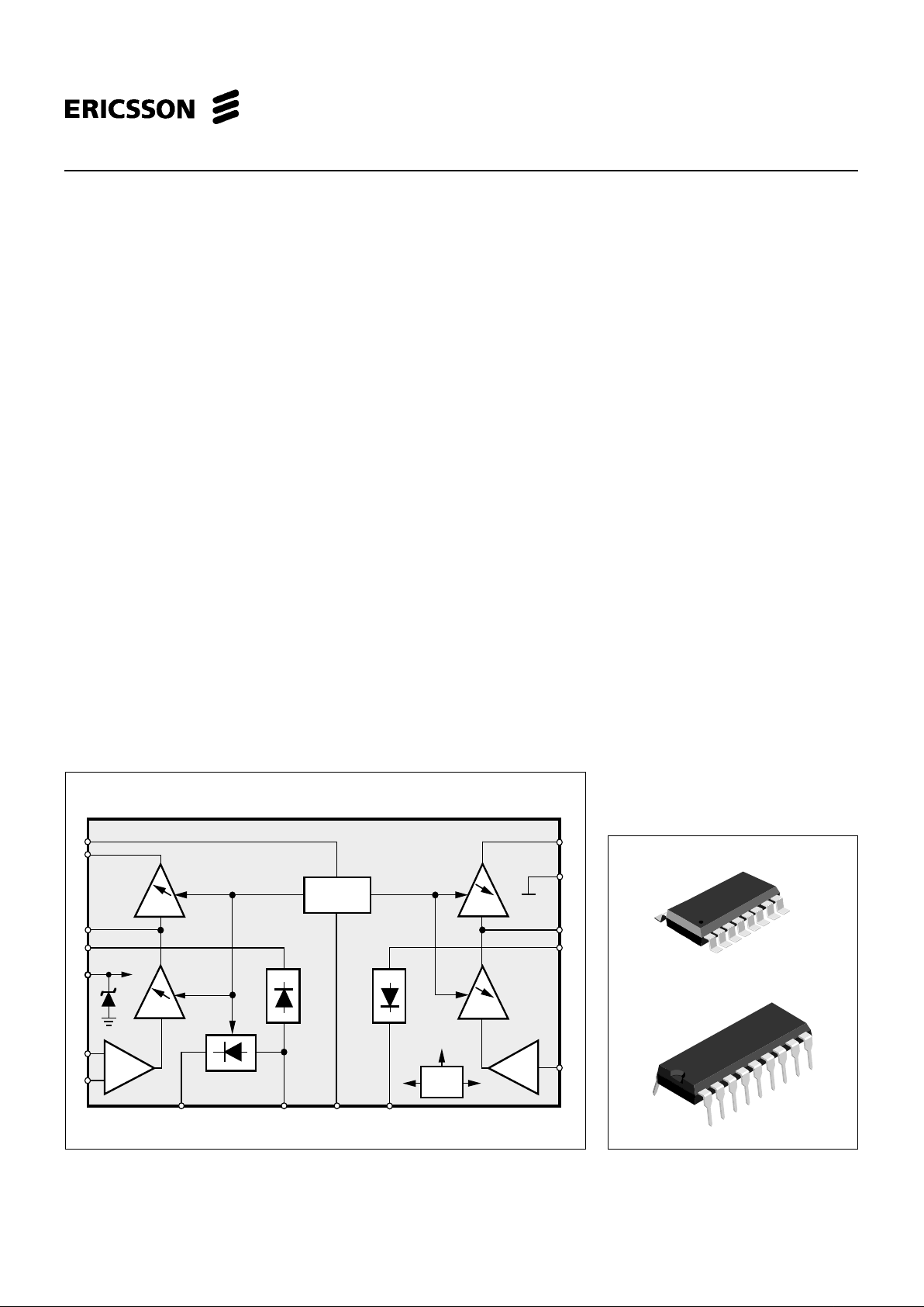
Figure 1. Block diagram. ( SO - package )
18-pin DIP
PBL388 12
Key Features
• Settable gain dynamics (25 or 50
dB).
• Low power consumption, totally
1.0mA at 3.3V typical.
• Background noise compensation in
the transmitting channel with hold
function.
• Exellent noise performance.
• Both channel input amplifiers have
balanced inputs.
• Minimum of external components
needed for function.
• 16-pin SO and 18-pin DIP
encapsulation.
All figures in this paper refer to 16-pin SO package.
PBL 388 12
2
Maximum Ratings
Parameter Symbol Min Max Unit
Speech switch supply current I
D
10 mA
Voltage pin 1-14 -0,5 Vpin
15
+0.5 V
Operating temperature T
Amb
-20 +70 °C
Storage temperature T
Stg
-55 +125 °C
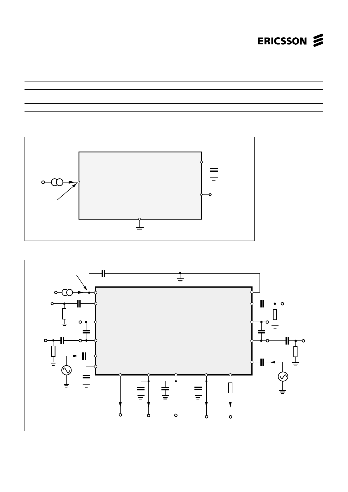
Figure 3. T est circuit. Reference figure No. 3.
Figure 2. Isolation and measurement of V
Ref
. Reference figure No.2.
CTR
V
V
CMP
V
TxDet
V
Rxout
CMP CTR
GND
79
10
1
16
8
Det
N
Tx
Detout
5
Tx
out
Rx
Detout
3
1 µF
Rxin
I
V
Rxin
+
NDet
R
CTR
C
TxDet
I
TxDet
0,1µF
C
RxDet
V
RxDet
I
CTR
V
NDet
RxDet
I
PBL 388 12
12
Rx
out
R
Rxout
10 µF
+
2
4
6
F2
out
14
100µF/16V
V
+
15
V
+
+
+
Tx
Detin
-Tx
in
+Tx
in
in
-Rx
11
Rx
Detin
13
F5
out
10 µF
+
F5
out
R
F5
out
C
Rx
V
Txout
+
10 µF
Txout
R
+
D
I
I
Txin
V
Txin
4.7 µF
+
1 µF
+
10 µF
+
F2
out
R
F2
out
C
Tx
+
V
+
GND
V
Ref
+
PBL 388 12
V
+
D
I
RxDetin
RxDetout 10
15
16
11
100nF

PBL 388 12
3
Electrical Characteristics
f = 1 kHz, T = 25°C, R
CTR
=0, C
TxDet
= 0, R
Txout
= ∞, R
Rxout
= ∞, R
F2out
= ∞, R
F5out
= ∞, RTx= 0, RRx= 0, C
RxDet
= 0 and
I
D
=1.0mA unless otherwise noted.
Ref.
Parameter fig. Condition Min. T yp. Max. Unit.
Speech control section
T erminal voltage, V
+
3ID = 1.0mA 3.3 V
Internal reference voltage, V
Ref
2 1.96 V
Frequency response for all amplifiers 3 200 - 3400 Hz, Relative 1 kHz -1 1 dB
Transmit gain, 20 •
10
log(V
Txout
/V
Txin
)3V
CMP
= V
Ref
- 0.1 V 41.5 44 dB
V
CMP
= V
Ref
+ 0.1 V -6 -3.5 dB
V
CMP
= V
Ref
- 0.1 V R
CTR
=100k, V
CTR
=V+ 41.5 44 dB
V
CMP
= V
Ref
+ 0.1 V R
CTR
=100k, V
CTR
=V+ 19 21.5 dB
Receive gain, 20 •
10
log(V
Rxout
/V
Rxin
)3V
CMP
= V
Ref
+ 0.1 V 26.5 29 dB
V
CMP
= V
Ref
- 0.1 V -21 -18.5 dB
V
CMP
= V
Ref
+ 0.1 V R
CTR
=100k, V
CTR
=V+ 26.5 29 dB
V
CMP
= V
Ref
- 0.1 V R
CTR
=100k, V
CTR
=V+ 4 6.5 dB
Max transmit detector gain, 3 V
TxDet
< 200 mVp , CTx = 100nF
20 •
10
log(V
Txdet
/V
Txin
)V
CMP
= V
Ref
- 0.1 V 67.5 dB
V
CMP
= V
Ref
+ 0.1 V 37 42.5 dB
Max receive detector gain, 3 V
RxDet
< 200 mVp , CTx = 100nF
20 •
10
log(V
Rxdet
/V
Rxin
)V
CMP
= V
Ref
+0.1 V 53 dB
V
CMP
= V
Ref
- 0.1 V 22.5 28 dB
Background noise rectifier gain, (note 1) 3 V
CMP
= V
Ref
- 0.1 V , C
Txdet
=1µF 6.0 dB
V
CMP
= V
Ref
+ 0.1 V , C
Txdet
=1µF Hold
+ Tx
In
input impedance 3 80 100 120 kΩ
- Tx
In
input impedance 3 2.4 3.0 3.6 kΩ
- Rx
In
input impedance 3 16 20 24 kΩ
Tx
Out
ac, load impedance 3 10 kΩ
Rx
Out
ac, load impedance 3 10 kΩ
F2
Out
ac, load impedance 3 10 kΩ
F5
Out
ac, load impedance 3 10 kΩ
Transmitter channel output swing, v
TxOut
3 2% distortion,R
Txout=RRxout
=25k Ω 500 mV
p
Receiver channel output swing, v
RxOut
3 2% distortion,R
Txout=RRxout
=25k Ω 500 mV
p
Transmitter output noise, v
TxOut
3V
CMP
= V
Ref
- 0.1 V , v
TxIn
= 0 V -75 dB
psof
Receiver output noise, v
RxOut
3V
CMP
= V
Ref
+ 0.1 V , v
RxIn
= 0 V -75 dB
A
Tx
Det
sink current, I
TxDetOut
3V
TxDetIn
= V
Ref
+ 0.1 V -6.0 -2.5 mA
Rx
Det
source current, I
RxDetOut
3V
RxIn
= V
Ref
- 0.1 V 2.5 6.0 mA
Tx
Det
source current, I
TxDet
3V
CMP
= V
Ref
- 0.1 V 30 µA
Rx
Det
sink current, I
RxDetOut
3V
RxDetIn
= V
Ref
+ 0.1 V -30 µA
Tx
Det
swing relative to V
Ref
, V
TxDetOut
3V
TxDetIn
= V
Ref
+ 0.1 V (note 2) -0.7 V
Rx
Det
swing relative to V
Ref
, V
RxDetOut
3V
RxDetIn
= V
Ref
- 0.1 V (note 2) +0.7 V
N
Det
sink current (fast charge), I
NDet
3V
TxDetIn
= V
Ref
- 0.1 V -4.5 -1.5 mA
V
CMP
= V
Ref
- 0.1 V
N
Det
source current, I
NDet
3V
TxDetIn
= V
Ref
+ 0.1 V 3 5 7 µA
V
CMP
= V
Ref
+ 0.1 V
 Loading...