

Ericsson PBL38661-2QNS, PBL38661-2QNT Datasheet
Description
The PBL 386 61/2 Subscriber Line Interface Circuit (SLIC) is a 90 V bipolar integrated
circuit for use in Central Office, MUX and other telecommunications equipment. The
PBL 386 61/2 has been optimized for low total line interface cost and a high degree of
flexibility in different applications.
The PBL 386 61/2 emulates a transformer equivalent dc-feed, programmable
between 2x25 Ω and 2x900 Ω, with short loop current limiting adjustable to max
65 mA.
A second lower battery voltage may be connected to the device to reduce short
loop power dissipation. The SLIC automatically switches between the two battery
supply voltages without need for external components or external control.
The SLIC incorporates loop current and ring trip detection functions. The
PBL 386 61/2 is compatible with loop start signalling.
Two- to four-wire and four- to two-wire voice frequency (vf) signal conversion is
accomplished by the SLIC in conjunction with either a conventional CODEC/filter or
with a programmable CODEC/filter, e.g. SLAC, SiCoFi, Combo II. The programmable
line terminating impedance could be complex or real to fit every market.
Longitudinal line voltages are suppressed by a feedback loop in the SLIC and the
longitudinal balance specifications meet Bellcore TR909 requirements.
The PBL 386 61/2 package is 28-pin PLCC.
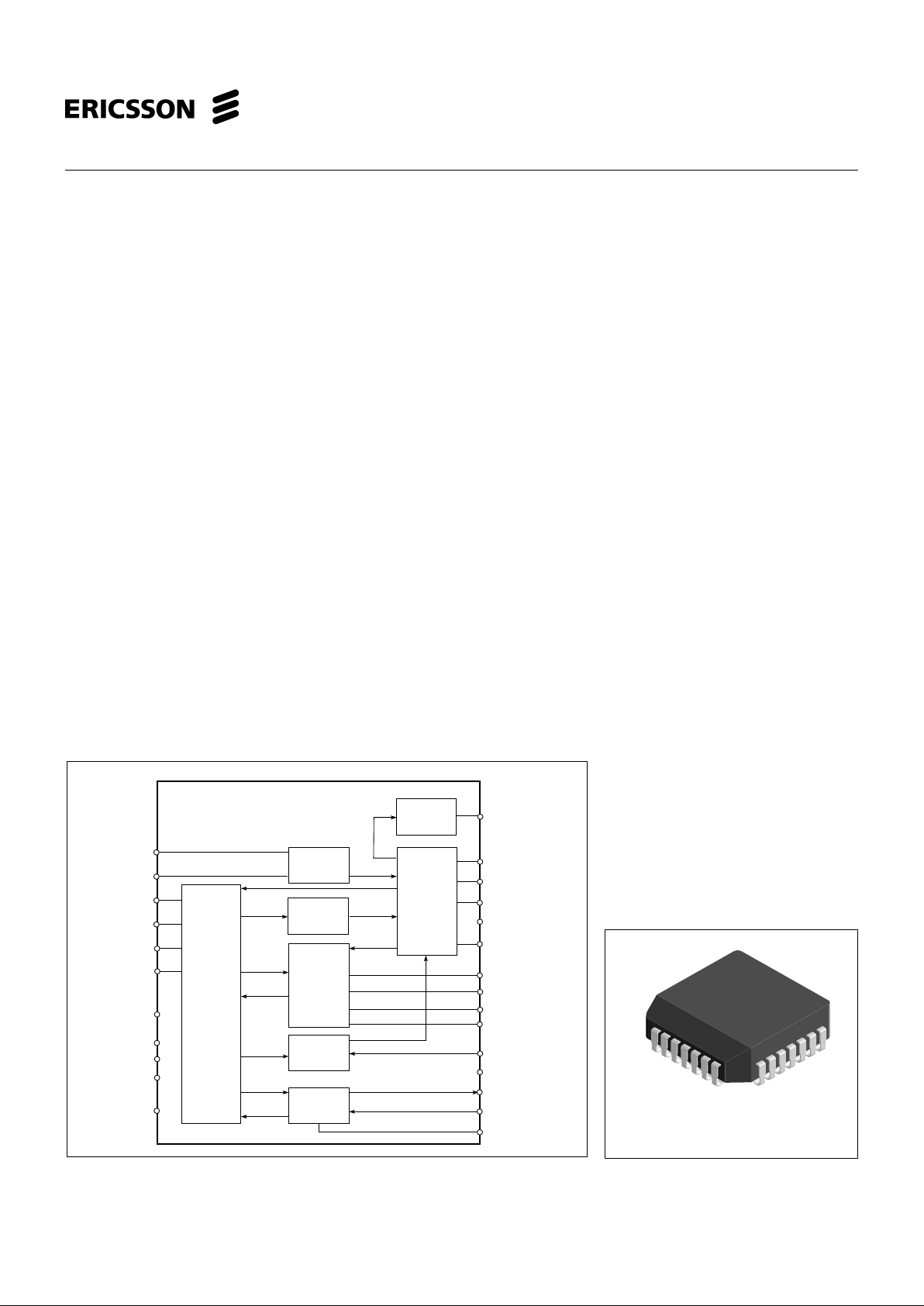
Figure 1. Block diagram.
February 2000
PBL 386 61/2
Subscriber Line
Interface Circuit
28-pin plastic PLCC
VF Signal
Transmission
Off-hook
Detector
Line Feed
Controller
and
Longitudinal
Signal
Suppression
Ring Trip
Two-wire
Interface
Input
Decoder and
Control
C1
C2
DET
REF
LP
VTX
RSN
DT
DR
TIPX
HP
RINGX
VCC
VEE
VBAT2
VBAT
AGND
C3
BGND
Comparator
Ground Key
Detector
Ring Relay
Driver
RRLY
PLD
PLC
PSGTS
AOV
VEE
PBL
386 61/2
Preliminary
Key Features
• Selectable overhead voltage principle
– All adaptive: The overhead voltage
follows 0.6 V
Peak
< signals < 6.2 V
Peak
.
– Semi adaptive: The overhead voltage
follows 3.1 V
Peak
< signals < 6.2 V
Peak
.
• Metering 2.2 V
rms
.
• High and low battery with automatic
switching
• Battery supply as low as -10 V
• Only +5 V in addition to GND
and battery (VEE optional)
• 39 mW on-hook power dissipation in
active state
• Long loop battery feed tracks V
Bat
for
maximum line voltage
• 44 V open loop voltage @ -48 V battery
feed
• Constant loop voltage for line
leakage <5 mA
• On-hook transmission
• Full longitudinal current capability
during on-hook
• Programmable loop & ring-trip detector
threshold
• Analog temperature guard
1

PBL 386 61/2
2
Preliminary
Maximum Ratings
Parameter Symbol Min Max Unit
Temperature, Humidity
Storage temperature range T
Stg
-55 +150 °C
Operating temperature range T
Amb
-40 +110 °C
Operating junction temperature range, Note 1 T
J
-40 +140 °C
Power supply, 0°C ≤ T
Amb
≤ +70°C
V
CC
with respect to AGND V
CC
-0.4 6.5 V
V
EE
with respect to AGND V
EE
V
Bat
0.4 V
V
Bat
with respect to BGND, continuous V
Bat
-75 0.4 V
V
Bat
with respect to BGND, 10 ms V
Bat
-80 0.4 V
V
Bat2
with respect to A/BGND V
Bat2
V
Bat2
0.4 V
Power dissipation
Continuous power dissipation at T
Amb
≤ +70 °CP
D
1.5 W
Ground
Voltage between AGND and BGND V
G
-5 VCC V
Relay Driver
Ring relay supply voltage BGND +13 V
Ring relay current 75 mA
Ring trip comparator
Input voltage V
DT
, V
DR
V
Bat
V
CC
V
Input current I
DT
, I
DR
-5 5 mA
Digital inputs, outputs (C1, C2, DET)
Input voltage V
ID
-0.4 V
CC
V
Output voltage (DET not active) V
OD
-0.4 V
CC
V
Output current (DET) I
OD
30 mA
TIPX and RINGX terminals, 0°C < T
Amb
< +70°C, V
Bat
= -50 V
TIPX or RINGX current I
TIPX
, I
RINGX
-110 +110 mA
TIPX or RINGX voltage, continuous (referenced to AGND), Note 2 V
TA
, V
RA
V
Bat
2V
TIPX or RINGX, pulse < 10 ms, t
Rep
> 10 s, Note 2 VTA, V
RA
V
Bat
- 20 5 V
TIPX or RINGX, pulse < 1 µs, t
Rep
> 10 s, Note 2 VTA, V
RA
V
Bat
- 40 10 V
TIP or RING, pulse < 250 ns, t
Rep
> 10 s, Note 3 VTA, V
RA
V
Bat
- 70 15 V
Recommended Operating Condition
Parameter Symbol Min Max Unit
Ambient temperature T
Amb
0 +70 °C
Maximum supplied V
CC
with respect to AGND V
CC
4.75 5.25 V
V
EE
with respect to AGND V
EE
V
Bat
-4.75 V
V
Bat
with respect to BGND V
Bat
-58 -10 V
V
Bat2
with respect to BGND V
Bat2
V
Bat
-10 V
Notes
1. The circuit includes thermal protection. Operation above max. junction temperature may degrade device reliability.
2. A diode in series with the VBat input increases the permitted continuous voltage and pulse < 10 ms to -85 V. A pulse
≤1µs is increased to the greater of |-70V| and |VBat -40V|.
3. R
F1
and RF2 ≥20 Ω are also required. Pulse is supplied to TIP and RING outside RF1 and RF2.
PBL 386 61/2
3
Preliminary
Electrical Characteristics
0 °C ≤ T
Amb
≤ +70 °C, VCC = +5V ±5 %, VEE = -5V ± 5%, V
Bat
= -58V to -40V, RLC=18.7kΩ, IL = 27 mA, ZL = 600 Ω, RF1, RF2 = 0 Ω,
R
Ref
= 15kΩ, CHP = 68nF, CLP=0.33 µF, RT = 120 kΩ, RSG = 24 kΩ, RRX = 120 kΩ, AOV and V
Bat2
pin not connected, unless
otherwise specified. Current definition: current is positive if flowing into a pin.
Ref
Parameter fig Conditions Min Typ Max Unit
Two-wire port
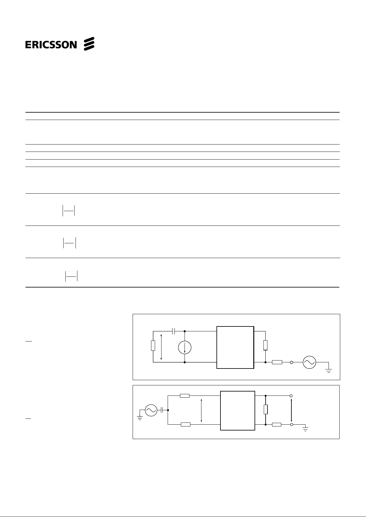
Overload level, V
TRO ,ILDC
> 10 mA 2 Active state
1% THD, Note 1 3.1 V
Peak
On-Hook, I
LDC
≤ 5 mA 1.4 V
Peak
Input impedance, Z
TR
Note 2 ZT/200
Longitudinal impedance, Z
LoT
, Z
LoR
0 < f < 100 Hz 20 35 Ω/wire
Longitudinal current limit, I
LoT
, I
LoR
active state 28 mA
rms
/wire
Longitudinal to metallic balance, B
LM
IEEE standard 455-1985, ZTRX = 736 Ω, active state
0.2 kHz < f < 1.0 kHz 55 dB
1.0 kHz < f < 3.4 kHz 55 dB
Longitudinal to metallic balance, B
LME
3 active state
E
Lo
B
LME
= 20 • Log 0.2 kHz ≤ f ≤ 1.0 kHz 55 dB
V
TR
1.0 kHz < f < 3.4 kHz 55 dB
Longitudinal to four-wire balance, B
LFE
3 active state
E
Lo
B
LFE
= 20 • Log 0.2 kHz ≤ f ≤ 1.0 kHz 61 dB
V
TX
1.0 kHz < f < 3.4 kHz 61 dB
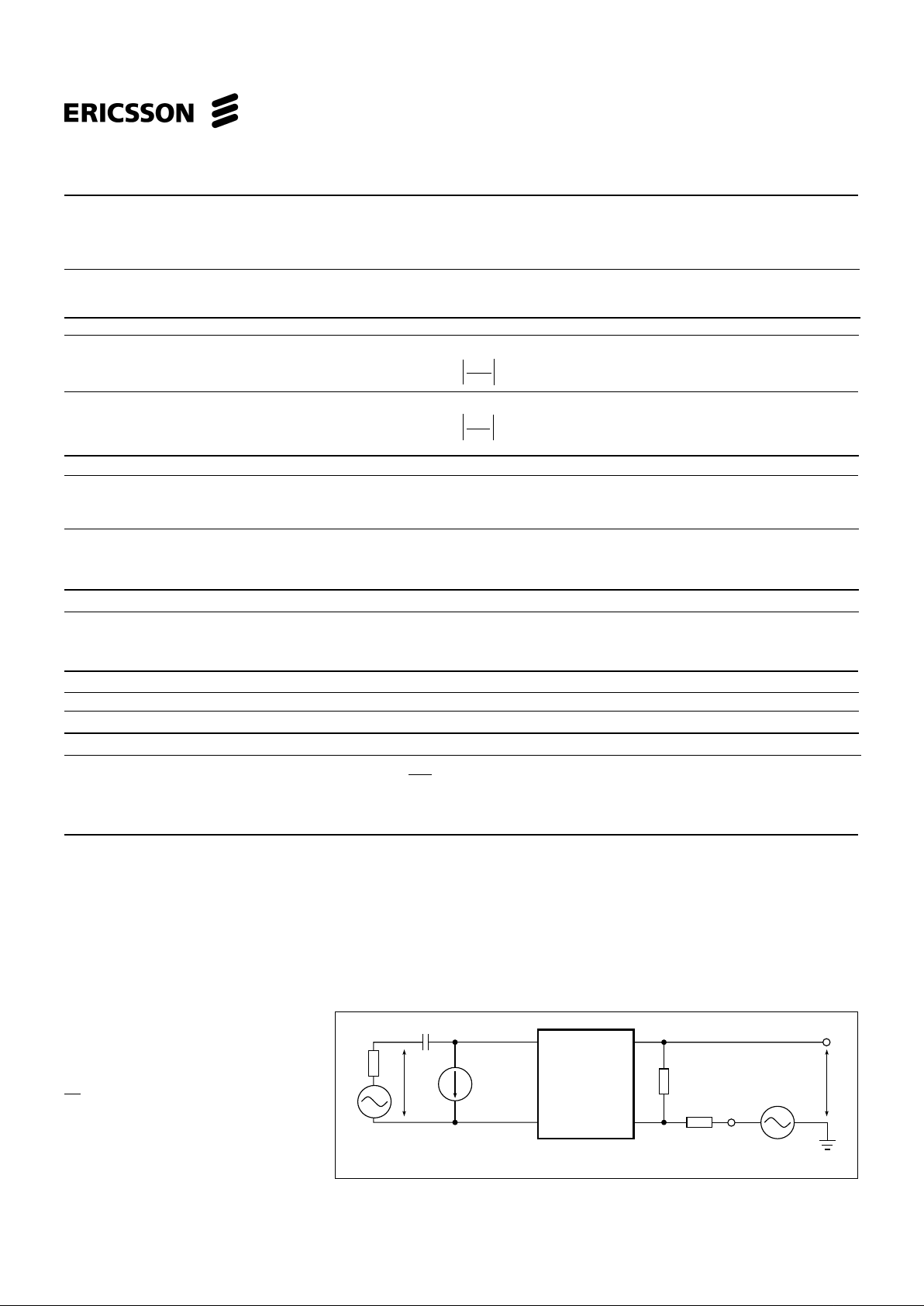
Metallic to longitudinal balance, B
MLE
4 active state
VTR
0.2 kHz < f < 3.4kHz 40 dB
B
MLE
= 20 • Log
V
Lo
Figure 2. Overload level, V
TRO
, two-wire
port
1
<< RL, RL= 600 Ω
ωC
RT = 120 kΩ, RRX = 120 kΩ
PBL 386 61/2
TIPX
RINGX
RSN
VTX
R
T
R
RX
E
RX
R
L
V
TRO
I
LDC
C
PBL 386 61/2
TIPX
RINGX RSN
VTX
R
T
R
RX
V
TX
R
LT
C
V
TR
R
LR
E
Lo
Figure 3. Longitudinal to metallic (B
LME
)
and Longitudinal to four-wire (B
LFE
)
balance
1
<< 150 Ω, R
LR
= RLT = RL /2= 300Ω
ωC
RT = 120 kΩ, RRX = 120 kΩ
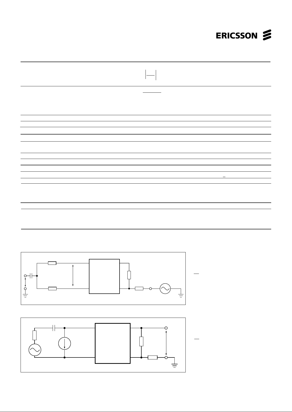
PBL 386 61/2
4
Preliminary
Parameter fig Conditions Min Typ Max Unit
Four-wire to longitudinal balance, B
FLE
4 active state
E
RX
B
FLE
= 20 • Log
V
Lo
0.2 kHz < f < 3.4 kHz 40 dB
Two-wire return loss, r |Z
TR
+ ZL|
r = 20 • Log
|Z
TR
- ZL|
0.2 kHz < f < 0.5 kHz 25 dB
0.5 kHz < f < 1.0 kHz 27 dB
1.0 kHz < f < 3.4 kHz, Note 3 23 dB
TIPX idle voltage, V
Ti
active, IL = 0 - 1.5 V
RINGX idle voltage, V
Ri
active, IL = 0 V
Bat+
2.7 V
V
TR
active, IL = 0 V
Bat
+4.2 V
Four-wire transmit port (VTX)
Overload level, I
LDC
≥ 10 mA 5 Load impedance > 20 kΩ, 1.55 V
Peak
On hook I
LDC
≤ 5 mA 1% THD, Note 4 0.7 V
Peak
Output offset voltage, ∆V
TX
-60 60 mV
Output impedance, z
TX
0.2 kHz < f < 3.4 kHz 5 20 Ω
Four-wire receive port (RSN)
Receive summing node (RSN) dc voltage I
RSN
= 0 mA GND +25 mV
Receive summing node (RSN) impedance 0.2 kHz < f < 3.4 kHz 10 50 Ω
Receive summing node (RSN) 0.3 kHz < f < 3.4 kHz
current (I
RSN
) to metallic loop current (IL) 400 ratio
gain,α
RSN
Frequency response
Two-wire to four-wire, g
2-4
6 relative to 0 dBm, 1.0 kHz. ERX = 0 V
0.3 kHz < f < 3.4 kHz -0.15 0.15 dB
f = 8.0 kHz, 12 kHz, 16 kHz -0.5 -0.1 0 dB
Figure 4. Metallic to longitudinal and
four-wire to longitudinal balance
1
<< 150 Ω, R
LT
= RLR = RL /2 =300Ω
ωC
RT = 120 kΩ, RRX = 120 kΩ
Figure 5. Overload level, V
TXO
, four-wire
transmit port
1
<< R
L
, RL = 600 Ω
ωC
R
T
= 120 kΩ, RRX = 120 kΩ
Ref
PBL 386 61/2
TIPX
RINGX RSN
VTX
R
T
R
RX
E
RX
R
LT
C
V
TR
R
LR
V
Lo
PBL 386 61/2
TIPX
RINGX RSN
VTX
R
T
R
RX
R
L
I
LDC
C
E
L
V
TXO
PBL 386 61/2
5
Preliminary
Four-wire to two-wire, g
4-2
6 relative to 0 dBm, 1.0 kHz. EL = 0 V
0.3 kHz < f < 3.4 kHz -0.15 0.15 dB
f = 8 kHz, 12 kHz, -1.0 -0.2 0 dB
16 kHz -1.0 -0.3 0 dB
Four-wire to four-wire, g
4-4
6 relative to 0 dBm, 1.0 kHz. EL = 0 V
0.3 kHz < f < 3.4 kHz -0.15 0.15 dB
Insertion loss
Two-wire to four-wire, G
2-4
6 0 dBm, 1.0 kHz, Note 5
V
TX
G
2-4
= 20 • Log ,ERX = 0
V
TR
-6.22 -6.02 -5.82 dB
Four-wire to two-wire, G
4-2
6 0 dBm, 1.0 kHz, Notes 5, 6
V
TR
G
4-2
= 20 • Log ,EL = 0
E
RX
-0.2 0.2 dB
Gain tracking
Two-wire to four-wire R
LDC
≤ 2kΩ 6 Ref. -10 dBm, 1.0 kHz, Note 7
-40 dBm to +3 dBm -0.1 0.1 dB
-55 dBm to -40 dBm -0.2 0.2 dB
Four-wire to two-wire R
LDC
≤ 2kΩ 6 Ref. -10 dBm, 1.0 kHz, Note 7
-40 dBm to +3 dBm -0.1 0.1 dB
-55 dBm to -40 dBm -0.2 0.2 dB
Noise
Idle channel noise at two-wire C-message weighting 7 12 dBrnC
(TIPX-RINGX) Psophometrical weighting -85 -78 dBmp
Note 8
Harmonic distortion
Two-wire to four-wire 6 0 dBm, 1.0 kHz test signal -50 dB
Four-wire to two-wire 0.3 kHz < f < 3.4 kHz -50 dB
Battery feed characteristics
Constant loop current, I
LConst
12 I
LProg
=
500
R
LC
18 < I
LProg
< 65 mA 0.92 I
LProgILProg
1.08 I
LProg
mA
Ref
Parameter fig Conditions Min Typ Max Unit
Figure 6.
Frequency response, insertion loss,
gain tracking.
1
<< R
L
, RL = 600 Ω
ωC
RT = 120 kΩ, RRX = 120 kΩ
PBL 386 61/2
TIPX
RINGX RSN
VTX
R
T
R
RX
E
RX
R
L
V
TR
I
LDC
C
E
L
V
TX

PBL 386 61/2
6
Preliminary
Loop current detector
Programmable threshold, I
DET
I
LTh
=
500 0.9•I
LThILTh
1.1•I
LTh
mA
R
LD
Ring trip comparator
Offset voltage, ∆V
DTDR
Source resistance, RS = 0 Ω -20 0 20 mV
Input bias current, I
B
IB = (IDT + IDR)/2 -50 -20 200 nA
Input common mode range, V
DT
, V
DR
V
Bat
+1 -1 V
Ring relay driver
Saturation voltage, V
OL
IOL = 50 mA 0.5 V
Off state leakage current, I
Lk
V
OH
= 12 V 100 µA
Digital inputs (C1, C2, C3)
Input low voltage, V
IL
0 0.5 V
Input high voltage, V
IH
2.5 V
CC
V
Input low current, I
IL
VIL = 0.5 -200 µA
Input high current, I
IH
VIH = 2.5 V 200 µA
Detector output (DET)
Output low current, I
OL
VOL < 0.6V 0.5 1 mA
Internal pull-up resistor 10 kΩ
Power dissipation (V
Bat
= -48V, V
Bat2
= -32V)
P
1
Open circuit state, C1, C2, C3 = 0, 0, 0 14 mW
P
2
@ VEE = -5V Active state, C1, C2, C3 = 0, 1, 0 39 mW
P
3
@ VEE = -48V Longitudinal current = 0 mA, IL = 0 mA 44 mW
P
4
@ VEE = -5V RL = 300Ω (off-hook) 710 mW
P
5
@ VEE = -5V RL = 800Ω (off-hook) 340 mW
Power supply currents (V
Bat
= -48V)
V
CC
current, I
CC
Open circuit state 0.8 mA
V
EE
current, I
EE
C1, C2, C3 = 0, 0, 0 -0.1 mA
V
Bat
current, I
Bat
-0.2 mA
V
CC
current, I
CC
Active state 2.0 mA
V
EE
current, I
EE
C1, C2, C3 = 0, 1, 0 0.1 mA
V
Bat
current, I
Bat
On-hook, Long Current = 0 mA, IL = 0 mA -0.7 mA
Power supply rejection ratios
V
CC
to 2- or 4-wire port Active State 28.5 35 dB
V
EE
to 2- or 4-wire port C1, C2, C3 = 0, 1, 0 28.5 55 dB
V
Bat
to 2- or 4-wire port 50 Hz < f< 3400 Hz, Vn = 100mV 28.5 40 dB
V
Bat2
to 2- or 4-wire port 28.5 60 dB
Temperature guard
Junction threshold temperature, T
JG
140 °C
Parameter fig Conditions Min Typ Max Unit
Ref
 Loading...