

Datasheet PBL38650-2QNS, PBL38650-2QNT, PBL38650-2SHT, PBL38650-2SOS, PBL38650-2SOT Datasheet (Ericsson)
Description
The PBL 386 50/2 Subscriber Line Interface Circuit (SLIC) is a 90 V bipolar integrated
circuit for use in Central Office Metering applications and other telecommunications
equipment. The PBL 386 50/2 has been optimized for low total line interface cost and
a high degree of flexibility in different applications.
The PBL 386 50/2 emulates resistive loop feed, programmable between 2x50 Ω
and 2x900 Ω, with short loop current limiting adjustable to max 45 mA. In the current
limited region the loop feed is nearly constant current with a slight slope
corresponding to 2x30kΩ.
A second, lower battery voltage may be connected to the device to reduce short
loop power dissipation. The SLIC automatically switches between the two battery
supply voltages without need for external components or external control.
The SLIC incorporates loop current, ground key and ring trip detection functions.
The PBL 386 50/2 is compatible with both loop and ground start signaling.
Two- to four-wire and four- to two-wire voice frequency (VF) signal conversion is
accomplished by the SLIC in conjunction with either a conventional CODEC/filter or
with a programmable CODEC/filter, e.g. SLAC, SiCoFi, Combo II. The programmable
two-wire impedance, complex or real, is set by a simple external network.
Longitudinal voltages are suppressed by a feedback loop in the SLIC and the
longitudinal balance specifications meet Bellcore TR909 requirements.
The PBL 386 50/2 package options are 24-pin SSOP, 24-pin SOIC or 28-pin PLCC.
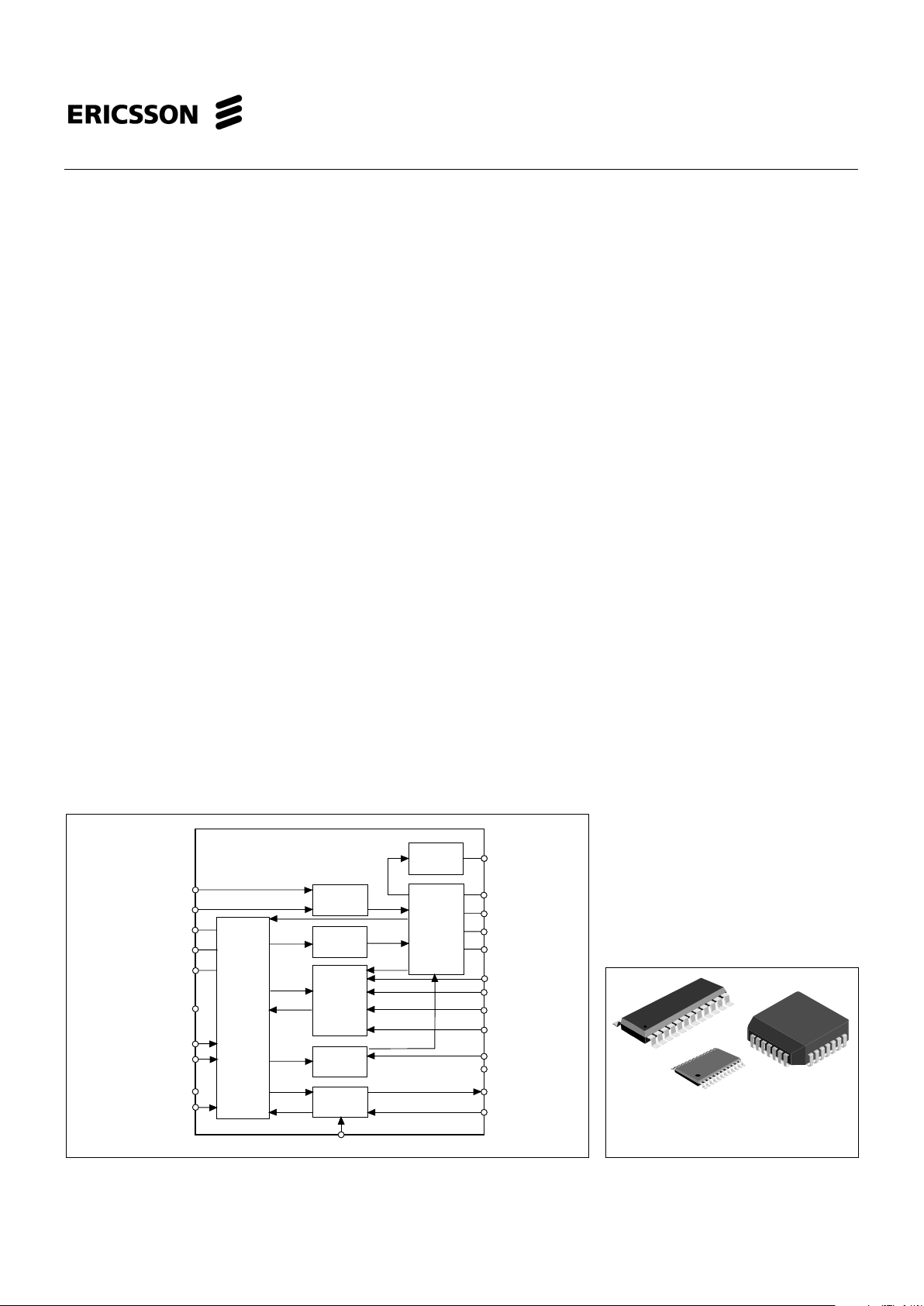
Figure 1. Block diagram.
June 1999
PBL 386 50/2
Subscriber Line
Interface Circuit
Key Features
• 24-pin SSOP package
• Programmable two-wire signal
headroom for 2.2 V
rms
metering
• High and low battery with automatic
switching
• Only +5 V feed in addition to battery
• Selectable transmit gain (0.5x or 0.25x)
• 70 mW on-hook power dissipation in
active state
• On-hook transmission
• Long loop battery feed tracks Vbat for
maximum line voltage
• No power-up sequence
• 43V open loop voltage @
-48V battery feed
• Constant loop voltage for line leakage
<5 mA (RLeak ~ >10 kΩ @ -48V)
• Full longitudinal current capability
during on-hook state
• Analog over temperature protection
permits transmission while the
protection circuit is active
• Line voltage measurement
• Polarity reversal
• Ground key detector
• Tip open state with ring ground
detector
24-pin SOIC, 24-pin SSOP, 28-pin PLCC
1
RRLY
C1
C2
C3
DET
PSG
REF
LP
PLD
PLC
VTX
RSN
PTG
BGND
AGND
VBAT
VBAT2
VCC
HP
RINGX
TIPX
DR
DT
Ring Relay
Driver
Input
Decoder
and
Control
Ring Trip
Comparator
Ground Key
Detector
Line Feed
Controller
and
Longitudinal
Signal
Suppression
Off-hook
Detector
VF Signal
Transmission
Two-wire
Interface
POV
PBL
386 50/2
PBL 386 50/2
PBL 386 50/2

PBL 386 50/2
2
Maximum Ratings
Parameter Symbol Min Max Unit
Temperature, Humidity
Storage temperature range T
Stg
-55 +150 °C
Operating temperature range T
Amb
-40 +110 °C
Operating junction temperature range, Note 1 T
J
-40 +140 °C
Power supply, 0°C ≤ T
Amb
≤ -70°C
V
CC
with respect to A/BGND V
CC
-0.4 6.5 V
V
Bat2
with respect to A/BGND V
Bat2
V
Bat
0.4 V
V
Bat
with respect to A/BGND, continuous V
Bat
-75 0.4 V
V
Bat
with respect to A/BGND, 10 ms V
Bat
-80 0.4 V
Power dissipation
Continuous power dissipation at T
Amb
≤ +70 °CP
D
1.5 W
Ground
Voltage between AGND and BGND V
G
-0,3 0,3 V
Relay Driver
Ring relay supply voltage BGND+14 V
Ring trip comparator
Input voltage V
DT
, V
DR
V
Bat
AGND V
Input current I
DT
, I
DR
-5 5 mA
Digital inputs, outputs (C1, C2, C3, DET)
Input voltage V
ID
-0.4 V
CC
V
Output voltage V
OD
-0.4 V
CC
V
TIPX and RINGX terminals, 0°C < T
Amb
< +70°C, V
Bat
= -50V
Maximum supplied TIPX or RINGX current I
TIPX
, I
RINGX
-100 +100 mA
TIPX or RINGX voltage, continuous (referenced to AGND), Note 2 VTA, V
RA
-80 2 V
TIPX or RINGX, pulse < 10 ms, t
Rep
> 10 s, Note 2 VTA, V
RA
V
Bat
-10 5 V
TIPX or RINGX, pulse < 1 µs, t
Rep
> 10 s, Note 2 VTA, V
RA
V
Bat
-25 10 V
TIPX or RINGX, pulse < 250 ns, t
Rep
> 10 s, Notes 2 & 3 VTA, V
RA
V
Bat
-35 15 V
Recommended Operating Condition
Parameter Symbol Min Max Unit
Ambient temperature T
Amb
0 +70 °C
V
CC
with respect to AGND V
CC
4.75 5.25 V
V
Bat
with respect to AGND V
Bat
-65 -8 V
AGND with respect to BGND V
G
-100 100 mV
Notes
1. The circuit includes thermal protection. Operation at or above 140°C junction temperature may degrade device reliability.
2. With the diodes D
VB
and D
VB2
included, see figure 12.
3. R
F1
and RF2 ≥ 20 Ω is also required. Pulse is applied to TIP and RING outside RF1 and RF2.
PBL 386 50/2
3
Figure 2. Overhead voltage, V
TRO
, two-
wire port
1
<< R
L
, RL= 600 Ω
ωC
R
T
= 60 kΩ, RRX = 60 kΩ
Electrical Characteristics
0 °C ≤ T
Amb
≤ +70 °C, PTG = Open (see pin description), ROV = ∞, VCC= +5V ±5 %, V
Bat
= -58V to -40V, V
Bat2
= -32V, RLC=32.4 kΩ, I
L
= 27 mA. RL = 600 Ω, RF1= RF2= RP1= RP2=0, R
Ref
= 49.9 kΩ, CHP = 47 nF, CLP=0.15 µF, RT = 60 kΩ, RSG = 0 kΩ, RRX = 60 kΩ, RR =
11 kΩ unless otherwise specified. Current definition: current is positive if flowing into a pin.
Ref
Parameter fig Conditions Min Typ Max Unit
Two-wire port
Overhead voltage, V
TRO ,ILdc
> 18mA 2 Active state, ROV = ∞ 2.7 V
Peak
0.2 kHz < f < 3.4 kHz
On-Hook, I
Ldc
< 5mA 1% THD, Note 1 1.1 V
Peak
Over load level, metering f≤16kHz, Z
LAC
=200Ω, Adj. by R
OV
5.0 V
Peak
Input impedance, Z
TR
Note 2 ZT/200
Longitudinal impedance, Z
LOT
, Z
LOR
0 < f < 100 Hz 20 35 Ω/wire
Longitudinal current limit, I
LOT
, I
LOR
active state 18 mA
rms
/wire
Longitudinal to metallic balance, B
LM
Normal polarity:
(IEEE standard 455-1985, Z
TRX
=736Ω) 0.2 kHz < f < 1.0 kHz 55 dB
Longitudinal to metallic balance, B
LME
3 1.0 kHz < f < 3.4 kHz 55 dB
Reverse polarity:
0.2 kHz < f < 3.4 kHz 55 dB
Longitudinal to four-wire balance, B
LFE
3 Normal polarity:
0.2 kHz < f < 1.0 kHz 61 75 dB
1.0 kHz < f < 3.4 kHz 61 70 dB
Reverse polarity:
0.2 kHz < f < 3.4 kHz 61 68 dB
Metallic to longitudinal balance, B
MLE
4 0.2 kHz < f < 3.4 kHz 40 50 dB
VTR
B
MLE
= 20 · Log ; ERX = 0
V
Lo
Figure 3. Longitudinal to metallic (B
LME
)
and Longitudinal to four-wire (B
LFE
)
balance
1
<< 150 Ω, R
LR =RLT
=RL /2=300Ω
ωC
RT = 60 kΩ, RRX = 60 kΩ
B
LFE
= 20 · Log
E
Lo
V
TR
B
LME
= 20 · Log
E
Lo
V
TX
PBL 386 50/2
TIPX
RINGX
RSN
VTX
R
T
R
RX
E
RX
R
L
V
TRO
I
LDC
C
PBL 386 50/2
TIPX
RINGX RSN
VTX
R
T
R
RX
V
TX
R
LT
C
V
TR
R
LR
E
Lo
PBL 386 50/2
4
Parameter fig Conditions Min Typ Max Unit
Four-wire to longitudinal balance, B
FLE
4 0.2 kHz < f < 3.4 kHz 40 50 dB
E
RX
B
FLE
= 20 · Log
V
Lo
Two-wire return loss, r |ZTR + ZL|
r = 20 · Log
|Z
TR
- ZL|
0.2 kHz < f < 1.0 kHz 27 35 dB
1.0 kHz < f < 3.4 kHz, Note 3 20 22 dB
TIPX idle voltage, V
Ti
active, IL <5 mA - 1.3 V
RINGX idle voltage, V
Ri
active, IL <5 mA V
Bat
+3.0 V
tip open, I
L
<5 mA V
Bat
+3.0 V
V
TR
active, IL<5 mA V
Bat
+4.3 V
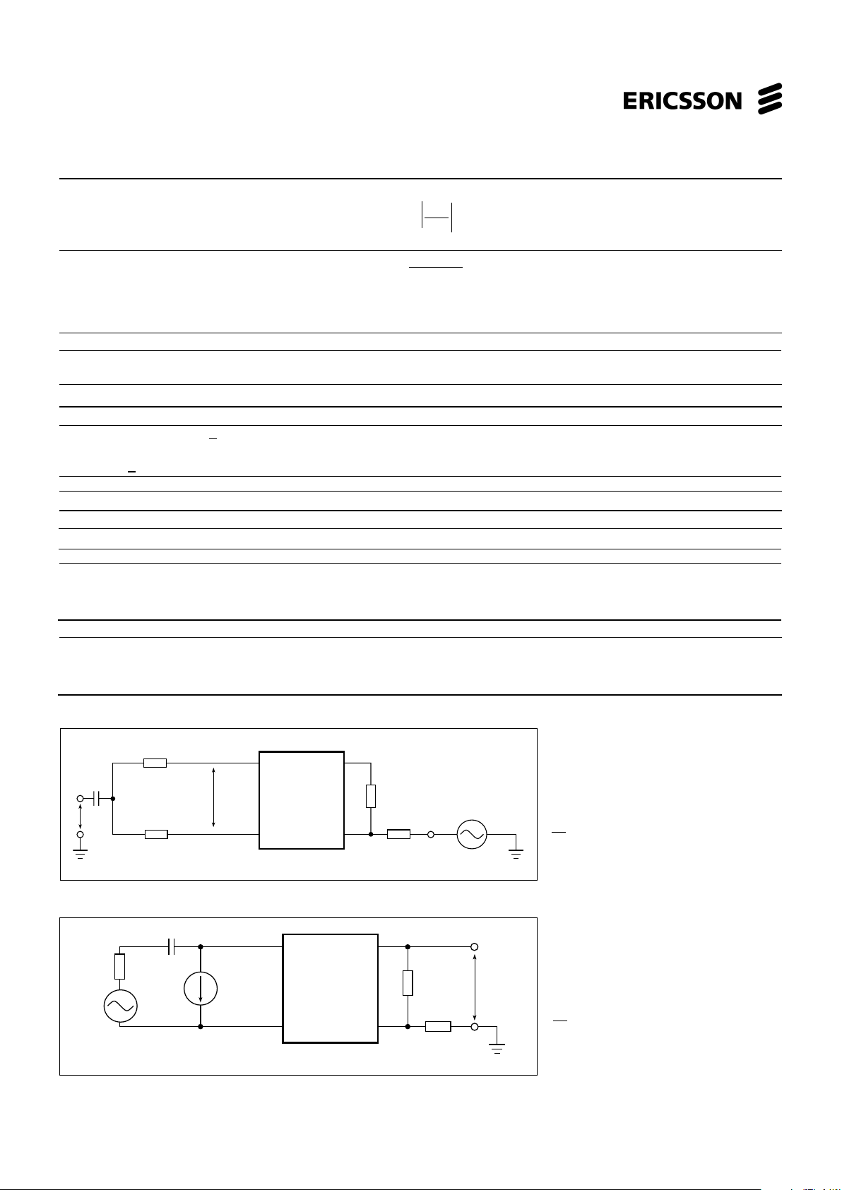
Four-wire transmit port (VTX)
Overhead voltage, V
TXO
, IL > 18mA 5 Load impedance > 20 kΩ, 1.35 V
Peak
1% THD, Note 4
On-hook, I
L
< 5mA 0.55 V
Peak
Output offset voltage, ∆V
TX
-100 0 100 mV
Output impedance, z
TX
0.2 kHz < f < 3.4 kHz 15 50 Ω
Four-wire receive port (RSN)
Receive summing node (RSN) DC voltage I
RSN
= -155 µA 1.15 1.25 1.35 V
Receive summing node (RSN) impedance 0.2 kHz < f < 3.4 kHz 8 20 Ω
Receive summing node (RSN) 0.3 kHz < f < 3.4 kHz
current (I
RSN
) to metallic loop current (IL) 200 ratio
gain,α
RSN
Frequency response
Two-wire to four-wire, g
2-4
6 relative to 0 dBm, 1.0 kHz. ERX = 0 V
0.3 kHz < f < 3.4 kHz -0.20 0.10 dB
f = 8.0 kHz, 12 kHz, 16 kHz -1.0 0.1 dB
Figure 4. Metallic to longitudinal and fourwire to longitudinal balance
1
<< 150 Ω, R
LT
=RLR =RL /2 =300Ω
ωC
R
T
= 60 kΩ, RRX = 60 kΩ
Figure 5. Overhead voltage, V
TXO
, four-
wire transmit port
1
<< R
L
, RL = 600 Ω
ωC
R
T
= 60 kΩ, RRX = 60 kΩ
Ref
PBL 386 50/2
TIPX
RINGX RSN
VTX
R
T
R
RX
E
RX
R
LT
C
V
TR
R
LR
V
Lo
PBL 386 50/2
TIPX
RINGX RSN
VTX
R
T
R
RX
R
L
I
LDC
C
E
L
V
TXO

PBL 386 50/2
5
Four-wire to two-wire, g
4-2
6 relative to 0 dBm, 1.0 kHz. EL=0 V
0.3 kHz < f < 3.4 kHz -0.2 0.1 dB
f = 8 kHz, 12 kHz, -1.0 0 dB
16 kHz -2.0 0 dB
Four-wire to four-wire, g
4-4
6 relative to 0 dBm, 1.0 kHz, EL=0 V
0.3 kHz < f < 3.4 kHz -0.2 0.1 dB
Insertion loss
Two-wire to four-wire, G
2-4
6 0 dBm, 1.0 kHz, Note 5
V
TX
G
2-4
= 20 · Log ; ERX = 0 -6.22 -6.02 -5.82 dB
V
TR
PTG = AGND -12.24 -12.04 -11.84 dB
Four-wire to two-wire, G
4-2
6 0 dBm, 1.0 kHz, Note 6
V
TR
G
4-2
= 20 · Log ; EL = 0 -0.2 0.2 dB
E
RX
Gain tracking
Two-wire to four-wire 6 Ref. -10 dBm, 1.0 kHz, Note 7
-40 dBm to +3 dBm -0.1 0.1 dB
-55 dBm to -40 dBm -0.2 0.2 dB
Four-wire to two-wire 6 Ref. -10 dBm, 1.0 kHz,
-40 dBm to +3 dBm -0.1 0.1 dB
-55 dBm to -40 dBm -0.2 0.2 dB
Noise
Idle channel noise at two-wire C-message weighting, 2 wire 12 dBrnC
(TIPX-RINGX) or four-wire (VTX) output Psophometrical weighting, 2 wire -78 dBmp
C-message weighting, 4 wire 6 dBrnC
Psophometrical weighting, 4 wire -84 dBmp
Note 8
Harmonic distortion
Two-wire to four-wire 6 0 dBm -67 -50 dB
Four-wire to two-wire 0.3 kHz < f < 3.4 kHz -67 -50 dB
Battery feed characteristics
Loop current, I
L
, in the current 13 18mA ≤ IL ≤ 45 mA 0.92 ILI
L
1.08 ILmA
limited region, reference A, B & C
Tip open state TIPX current, I
Leak
7 S = closed; R = 7 kΩ, Note 10 -150 µA
Tip open state RINGX current, I
LRTo
R
LRTo
= 0Ω, V
Bat
= -48V I
L
mA
R
LRTo
= 2.5 kΩ, V
Bat
= -48V 17 mA
Tip open state RINGX voltage, V
RTo
I
LRTo
< 23 mA V
Bat
+6 V
Ref
Parameter fig Conditions Min Typ Max Unit
Figure 6.
Frequency response, insertion loss,
gain tracking.
1
<< R
L
, RL = 600 Ω
ωC
R
T
= 60 kΩ, RRX = 60 kΩ
PBL 386 50/2
TIPX
RINGX RSN
VTX
R
T
R
RX
E
RX
R
L
V
TR
I
LDC
C
E
L
V
TX

PBL 386 50/2
6
Tip voltage (ground start) 7 Active state, Tip lead open (S open), -4 -2.2 V
Ring lead to ground through 150 Ω
Tip voltage (ground start) Active state, tip lead to -48 V -6 -2.4 V
through 7 kΩ (S closed), Ring
lead to ground through 150 Ω
Open circuit state loop current, I
LOC
RL = 0Ω -100 0 100 µA
Loop current detector
Programmable threshold, I
LTh
,I
LTh
=
500
0.85·I
LThILTh
1.15·I
LTh
mA
active, active reverse
R
LD
RLD in kΩ, I
LTh
≥ 7 mA
Tip open state
I
LTh
=
500 0.85·I
LThILTh
1.15·I
LTh
mA
R
LD
Ground key detector
Ground key detector threshold
(I
LTIPX
and I
LRINGX
difference to trigger ground key det.) 10 16 22 mA
Line voltage measurement
Pulse width, t
LVM
Note 9 5.5 µs/V
Ring trip comparator
Offset voltage, ∆V
DTDR
Source resistance, RS = 0 Ω -20 0 20 mV
Input bias current, I
B
IB = (IDT + IDR)/2 -200 -20 200 nA
Input common mode range, V
DT
, V
DR
V
Bat
+1 -1 V
Ring relay driver
Saturation voltage, V
OL
IOL = 50 mA 0.2 0.5 V
Off state leakage current, I
Lk
V
OH
= 12 V 10 µA
Digital inputs (C1, C2, C3)
Input low voltage, V
IL
0 0.5 V
Input high voltage, V
IH
2.5 V
CC
V
Input low current, I
IL
VIL = 0.5 -50 µA
Input high current, I
IH
VIH = 2.5 V 50 µA
Detector output (DET)
Output low voltage I
OL
= 0.5 mA 0.7 V
Internal pull-up resistor 15 kΩ
Power dissipation (V
Bat
= -48V, V
Bat2
= -32V)
P
1
Open circuit state, C1, C2, C3 = 0, 0, 0 10 15 mW
Active state, C1, C2, C3 = 0, 1, 0
P
2
Longitudinal current = 0 mA, I L=0 mA (on-hook) 70 85 mW
P
3
RL = 300 Ω (off-hook) 730 mW
P
4
RL = 800 Ω (off-hook) 360 mW
Power supply currents (V
Bat
= -48V)
V
CC
current, I
CC
Open circuit state 1.2 2.0 mA
V
Bat
current, I
Bat
-0.1 -0.05 mA
V
CC
current, I
CC
Active state 2.8 4.0 mA
V
Bat
current, I
Bat
On-hook, Long Current = 0 mA -1.5 -1.1 mA
Power supply rejection ratios
V
CC
to 2- or 4-wire port Active State 30 42 dB
V
Bat
to 2- or 4-wire port f = 1 kHz Vn = 100mV 36 45 dB
V
Bat2
to 2- or 4-wire port 40 60 dB
Temperature guard
Junction threshold temperature, T
JG
145 °C
Thermal resistance
28-pin PLCC, θ
JP28plcc
39 °C/W
24-pin SOIC, θ
JP24soic
43 °C/W
24-pin SSOP, θ
JP24ssop
55 °C/W
Parameter fig Conditions Min Typ Max Unit
Ref

PBL 386 50/2
7
Notes
1. The overhead voltage can be adjusted with the R
OV
resistor
for higher levels e.g. min 3.1 V
Peak
and is specified at the
two-wire port with the signal source at the four-wire
receive port.
2. The two-wire impedance is programmable by selection of
external component values according to:
Z
TRX
= ZT/|G
2-4S α RSN
| where:
Z
TRX
= impedance between the TIPX and RINGX
terminals
ZT= programming network between the VTX and RSN
terminals
G
2-4S
= transmit gain, nominally = 0.5 (or 0.25 see pin
PTG)
α
RSN
= receive current gain, nominally = 200 (current
defined as positive flowing into the receivesumming node, RSN, and when flowing from ring to tip).
3. Higher return loss values can be achieved by adding a
reactive component to RT, the two-wire terminating
impedance programming resistance, e.g. by dividing R
T
into two equal halves and connecting a capacitor from the
common point to ground.
4. The overhead voltage can be adjusted with the ROV
resistor for higher levels e.g. min 1.6 V
Peak
and is specified
at the four-wire transmit port, VTX, with the signal source
at the two-wire port. Note that the gain from the two-wire
port to the four-wire transmit port is G
2-4S
= 0.5 (or 0.25 see
pin PTG). The overhead voltage is dependent on G
2-4S
and
POV setting.
5. Pin PTG = Open sets transmit gain to nom. -6.02dB
Pin PTG = AGND sets transmit gain to nom. -12.04 dB
Secondary protection resistors R
F
and resistors RP impact
the insertion loss as explained in the text, section
Transmission. The specified insertion loss is for RF = RP = 0.
6. The specified insertion loss tolerance does not include
errors caused by external components.
7. The level is specified at the two-wire port.
8. The two-wire idle noise is specified with the port
terminated in 600 Ω (R
L
) and with the four-wire receive
port grounded (E
RX
= 0; see figure 6).
The four-wire idle noise at VTX is specified with the twowire port terminated in 600 Ω (RL). The noise specification
is referenced to a 600 Ω programmed two-wire impedance
level at VTX. The four-wire receive port is grounded
(E
RX
= 0).
9. Previous state must be active - loop or ground key
detector.
10. If |V
BExt
| ≥ |V
Bat
+ 2 V|, where V
Bat
is the voltage at V
BAT
pin,
the current I
Leak
is limited to ≈ 5mA.
Figure 7. Tipx voltage.
PBL 386 50/2
TIPX
RINGX
S
V
BExt
R
LRTo
R

PBL 386 50/2
8
Pin Description
Figure 8. Pin configuration, 24-pin SSOP, 24-pin SOIC and 28 pin PLCC package, top view.
Refer to figure 8.
PLCC Symbol Description
1 PTG Progr.Transmit Gain. Left open transmit gain = -6.02 dB, connected to AGND transmit gain = -12.04 dB.
2 RRLY Ring Relay driver output. The relay coil may be connected to maximum +14V.
3 HP Connection for High Pass filter capacitor, C
HP
. Other end of CHP connects to TIPX.
4NCNo internal Connection
5 RINGX The TIPX and RINGX pins connect to the tip and ring leads of the two-wire interface via overvoltage
protection components and ring relay (and optional test relay).
6 BGND Battery Ground, should be tied together with AGND.
7 TIPX The TIPX and RINGX pins connect to the tip and ring leads of the two-wire interface via overvoltage
protection components and ring relay (and optional test relay).
8 VBAT Battery supply Voltage. Negative with respect to AGND.
9 VBAT2 An optional second (2) Battery Voltage connects to this pin.
10 PSG Programmable Saturation Guard. The resistive part of the DC feed characteristic is programmed by a
resistor connected from this pin to VBAT.
11 NC No internal Connection
12 LP Connection for Low Pass filter capacitor, C
LP
. Other end of CLP connects to VBAT.
13 DT Input to the ring trip comparator. With DR more positive than DT the detector output, DET, is at logic level
low, indicating off-hook condition. The external ring trip network connects to this input.
14 DR Input to the ring trip comparator. With DR more positive than DT the detector output, DET, is at logic
level low, indicating off-hook condition. The external ring trip network connects to this input.
1
2
3
4
5
6
7
8
9
10
11
24
23
22
21
20
19
18
17
16
15
14
RRLY
PTG
HP
RINGX
BGND
TIPX
VBAT
LP
POV
VTX
AGND
C2
RSN
REF
PLD
VCC
C1
DT
PSG
PLC
VBAT2
DET
12
13
DR
C3
24-pin SOIC
and
24-pin SSOP
5
6
7
8
9
10
11
25
24
23
22
21
20
19
4
3
2
1
28
27
26
12
13
14
15
16
17
18
PTG
RRLY
HP
NC
BGND
TIPX
VBAT
VBAT2
PSG
LP
NC
DT
DR
C3
C2
C1
DET
NC
PLD
POV
PLC
REF
NC
AGND
VTX
RSN
VCC
RINGX
28-pin PLCC

PBL 386 50/2
9
15 C3
C1, C2 and C3 are digital inputs (internal pull-up) controlling the SLIC operating states.
16 C2
Refer to section "Operating states" for details.
17 C1
18 DET Detector output. Active low when indicating loop detection and ring trip, active high when indicating
ground key detection.
19 NC No internal Connection
20 VCC +5 V power supply.
21 PLD Programmable Loop Detector threshold. The loop detection threshold is programmed by a resistor
connected from this pin to AGND.
22 POV Programmable Overhead Voltage. If pin is left open: The overhead voltage is internally set to min 2.7 V in
off-hook and min 1.1 V in On-hook. If a resistor is connected between this pin and AGND: the overhead
voltage can be set to higher values.
23 PLC Prog. Line Current, the current limit,reference C in figure 13, is programmed by a resistor connected from
this pin to AGND.
24 REF A Reference, 49.9 kΩ, resistor should be connected from this pin to AGND.
25 NC No internal Connection
26 RSN Receive Summing Node. 200 times the AC-current flowing into this pin equals the metallic (transversal)
AC-current flowing from RINGX to TIPX. Programming networks for two-wire impedance and receive gain
connect to the receive summing node. A resistor should be connected from this pin to AGND.
27 AGND Analog Ground, should be tied together with BGND.
28 VTX Transmit vf output. The AC voltage difference between TIPX and RINGX, the AC metallic voltage, is
reproduced as an unbalanced GND referenced signal at VTX with a gain of 0.5 (or 0.25, see pin PTG).
The two-wire impedance programming network connects between VTX and RSN.
SLIC Operating States
State C3 C2 C1 SLIC operating state Active detector
0000 Open circuit 1001 Ringing state Ring trip detector (active low)
2010 Active state Loop detector (active low)
3011 Active state Line voltage measurement (note 9)
4100 Tip open state Loop detector (active low)
5101 Active state Ground key detector (active high)
6110 Active reverse Loop detector (active low)
7111 Active reverse Ground key detector (active high)
Table 1. SLIC operating states.
}

PBL 386 50/2
10
Four-Wire to Two-Wire Gain
From (1), (2) and (3) with E
L
= 0:
For applications where
Z
T
/(α
RSN·G2-4S
) + 2RF + 2RP is chosen to
be equal to ZL the expression for G
4-2
simplifies to:
Four-Wire to Four-Wire Gain
From (1), (2) and (3) with EL = 0:
Hybrid Function
The hybrid function can easily be
implemented utilizing the uncommitted
amplifier in conventional CODEC/filter
combinations. Please, refer to figure 10.
Via impedance Z
B
a current proportional
to VRX is injected into the summing node
of the combination CODEC/filter amplifier. As can be seen from the expression
for the four-wire to four-wire gain a
voltage proportional to VRX is returned to
VTX. This voltage is converted by RTX to a
current flowing into the same summing
node. These currents can be made to
cancel by letting:
The four-wire to four-wire gain, G
4-4
,
includes the required phase shift and
thus the balance network ZB can be
calculated from:
When choosing R
TX
, make sure the
output load of the VTX terminal is >20kΩ.
Functional Description
and Applications
Information
Transmission
General
A simplified ac model of the transmission circuits is shown in figure 9. Circuit
analysis yields:
(1)
(2)
V
TR
= EL - IL · Z
L
(3)
where:
V
TX
is a ground referenced version of
the ac metallic voltage between the
TIPX and RINGX terminals.
G
2-4S
is the programmable SLIC two-wire
to four-wire gain (transmit
direction). See note below.
V
TR
is the ac metallic voltage between
tip and ring.
E
L
is the line open circuit ac metallic
voltage.
I
L
is the ac metallic current.
R
F
is a fuse resistor.
R
P
is part of the SLIC protection
Z
L
is the line impedance.
VZV
Z
I
TXTRX
RXLRSN
+=
α
ZTdetermines the SLIC TIPX to
RINGX impedance at voice
frequencies.
Z
RX
controls four- to two-wire gain.
V
RX
is the analog ground referenced
receive signal.
α
RSN
is the receive summing node current
to metallic loop current gain = 200.
Note that the SLICs two-wire to four-
wire gain, G
2-4S
, is user programmable
between two fix values. Refer to the
datasheets for values on G
2-4S
.
Two-Wire Impedance
To calculate ZTR, the impedance
presented to the two-wire line by the
SLIC including the fuse and protection
resistors RF and RP, let VRX = 0.
From (1) and (2):
Thus with Z
TR
, α
RSN
, G
2-4S
, RP and R
F
known:
Two-Wire to Four-Wire Gain
From (1) and (2) with V
RX
= 0:
V
V
G
IR R
TR
TX
S
LFP
=+⋅+
−24
22()
Z
Z
G
RR
TR
T
RSN S
FP
=
⋅
++
−α24
22
ZGZRR
T RSN S TR F P
=⋅ ⋅−−
−α24
22()
G
V
V
Z
Z
G
RR
TX
TR
T RSN
T
RSN S
FP
24
24
22
−
−
==
⋅
++
/ α
α
Figure 9. Simplified ac transmission circuit.
V
R
V
Z
E
TXTXRX
B
L
+==00()
G
Z
ZG
T
RX S4224
1
2
−
−
=− ⋅
G
V
V
Z
Z
Z
Z
GZRR
TR
RX
T
RX
L
T
RSN
SL F P
42
24
22
−
−
==
−⋅
+⋅++
α
()
G
V
V
Z
Z
GZRR
Z
GZRR
TX
RX
T
RX
SL F P
T
RSN
SL F P
44
24
24
22
22
−
−
−
==
−⋅
⋅+ +
+⋅++
()
()
α
ZR
V
V
R
Z
Z
Z
GZRR
GZRR
BTX
RX
TX
TX
RX
T
T
RSN
SL F P
SL F P
=− ⋅ =
⋅⋅
+⋅++
⋅++
−
−
α
24
24
22
22
()
()
PBL 386 50/2
+
-
+
-
VTX
RSN
I
L
/
α
RSN
TIPX
RINGX
+
-
E
L
+
-
TIP
RING
R
F
R
F
Z
TR
Z
T
V
TX
V
RX
Z
RX
I
L
I
L
R
HP
+
-
Z
L
V
TR
R
P
G
2-4S
R
P

PBL 386 50/2
11
ance) forms the total two wire output
impedance of the SLIC. The choise of
these programmable components have
an influence on the power supply
rejection ratio (PSRR) from VBAT to the
two wire side at sub-audio frequencies.
At these frequencies capacitor CLP also
influences the transversal to longitudinal
balance in the SLIC. Table 1 suggests
suitable values on CLP for different
feeding characteristics. Typical values of
the transversal to longitudinal balance
(T-L bal.) at 200Hz is given in table 1 for
the chosen values on CLP.
R
Feed
R
SG
C
LP
T-L bal. C
HP
@200Hz
[
Ω
][kΩ] [nF] [dB] [nF]
2·50 0 150 -46 47
2·200 60.4 100 -46 150
2·400 147 47 -43 150
2·800 301 22 -36 150
Table 1. R
SG
, CLP and CHP values for
different feeding characteristics.
Figure 10. Hybrid function.
If calculation of the ZB formula above
yields a balance network containing an
inductor, an alternate method is recommended. Contact Ericsson Microelectronics for assistance.
The PBL 386 50/2 SLIC may also be
used together with programmable
CODEC/filters. The programmable
CODEC/filter allows for system controller
adjustment of hybrid balance to accommodate different line impedances without
change of hardware. In addition, the
transmit and receive gain may be
adjusted. Please, refer to the programmable CODEC/filter data sheets for
design information.
Longitudinal Impedance
A feed back loop counteracts longitudinal voltages at the two-wire port by
injecting longitudinal currents in opposing
phase.
Thus longitudinal disturbances will
appear as longitudinal currents and the
TIPX and RINGX terminals will experience very small longitudinal voltage
excursions, leaving metallic voltages well
within the SLIC common mode range.
The SLIC longitudinal impedance per
wire, Z
LoT
and Z
LoR
, appears as typically
20Ω to longitudinal disturbances. It
should be noted that longitudinal currents
may exceed the dc loop current without
disturbing the vf transmission.
Capacitors C
TC
and C
RC
The capacitors designated CTC and C
RC
in figure 12, connected between TIPX
and ground as well as between RINGX
and ground, can be used for RFI filtering.
The recommended value for C
TC
and
CRC is 2200 pF. Higher capacitance
values may be used, but care must be
taken to prevent degradation of either
longitudinal balance or return loss. C
TC
and CRC contribute to a metallic impedance of 1/(π·f·CTC) = 1/(π·f·CRC), a TIPX to
ground impedance of 1/(2·π·f·CTC) and a
RINGX to ground impedance of
1/(2·π·f·CRC).
AC - DC Separation Capacitor, C
HP
The high pass filter capacitor connected between terminals HP and TIPX
provides the separation of the ac signal
from the dc part. CHP positions the low
end frequency response break point of
the ac loop in the SLIC. Refer to table 1
for recommended values of CHP.
Example: A C
HP
value of 150 nF will
position the low end frequency response
3dB break point of the ac loop at 1.8 Hz
(f
3dB
) according to f
3dB
= 1/(2·π·RHP·CHP)
where RHP = 600 kΩ.
High-Pass Transmit Filter
The capacitor CTX in figure 12 connected between the VTX output and the
CODEC/filter forms, together with R
TX
and/or the input impedance of a programmable CODEC/filter, a high-pass
RC filter. It is recommended to position
the 3 dB break point of this filter between
30 and 80 Hz to get a faster response for
the dc steps that may occur at DTMF
signalling.
Capacitor C
LP
The capacitor CLP, which connects
between the terminals CLP and VBAT,
positions together with the resistive loop
feed resistor RSG (see section Battery
Feed), the high end frequency break
point of the low pass filter in the dc loop
in the SLIC. CLP together with RSG, C
HP
and ZT (see section Two-Wire Imped-
V
T
Combination
CODEC/Filter
R
TX
R
FB
Z
B
Z
RX
Z
T
VTX
RSN
V
RX
PBL
386 50/2

PBL 386 50/2
12
receive output via the resistor RRX, is dc
biased with +1.25V. This makes it
possible to compensate for currents
floating due to dc voltage differences
between RSN and the CODEC output
without using any capacitors. This is
done by connecting a resistor RR between the RSN terminal and ground.
With current directions defined as in
figure 14, current summation gives:
where V
CODEC
is the reference voltage of
the CODEC at the receive output.
From this equation the resistor R
R
can be
calculated as
For values on I
RSN
, see table 3.
The resistor R
R
has no influence on the
ac transmission.
SLIC I
RSN
[µA]
PBL 386 50/2 -155
Table 3. The SLIC internal bias current
with the direction of the current defined
as positive when floating into the terminal
RSN.
Programmable overhead voltage(POV)
With the POV function the overhead
voltage can be increased.
If the POV pin is left open the overhead
voltage is internally set to 3.2 V
Peak
in off-
The current limit (reference C in figure
13) is adjusted by connecting a resistor,
RLC, between terminal PLC and ground
according to the equation:
RLC =
1000
I
LProg
+ 4
where RLC is in kΩ for I
LProg
in mA.
A second, lower battery voltage may be
connected to the device at terminal
VBAT2 to reduce short loop power
dissipation. The SLIC automatically
switches between the two battery supply
voltages without need for external
control. The silent battery switching
occurs when the line voltage passes the
value |VB2| - 40·I
L
- (V
OHVirt
-1.3),
if IL > 6 mA.
For correct functionality it is important
to connect the terminal VBAT2 to the
second power supply via the diode D
VB2
in figure 12.
An optional diode D
BB
connected
between terminal VB and the VB2 power
supply, see figure 12, will make sure that
the SLIC continues to work on the
second battery even if the first battery
voltage disappears.
If a second battery voltage is not used,
VBAT2 is connected to VBAT on the
SLIC and C
VB2
, DBB and D
VB2
are removed.
Metering applications
For designs with metering applications
please contact Ericsson Microelectronics
for assistance.
CODEC Receive Interface
The PBL 386 50/2 SLIC have got a
completely new receive interface at the
four wire side which makes it possible to
reduce the number of capacitors in the
applications and to fit both single and
dual battery feed CODECs. The RSN
terminal, connecting to the CODEC
−=+ +=
+
−
+
IIII
R
V
RR
RSN RT RRX RR
T
CODEC
RX R
125 125 125,, ,
R
I
R
V
R
R
RSN
T
CODEC
RX
=
−− −
−
125
125
125
,
,
,
Battery Feed
The PBL 386 50/2 SLIC emulate
resistive loop feed, programmable
between 2·50Ω and 2·900 Ω, with
adjustable current limitation. In the
current limited region the loop current
has a slight slope corresponding to
2·30 kΩ, see figure 13 reference B.
The open loop voltage measured
between the TIPX and RINGX terminals
is tracking the battery voltage V
Bat
. The
signalling headroom, or overhead voltage
V
TRO
, is programmable with a resistor R
OV
connected between terminal POV on the
SLIC and ground. Please refer to section
“Programmable overhead voltage(POV)”.
The battery voltage overhead, V
OH
,
depends on the programmed signal
overhead voltage V
TRO
. VOH defines the
TIP to RING voltage at open loop
conditions according to VTR(at IL = 0 mA)
= |V
Bat
| - VOH.
Refer to table 2 for typical values on
V
OH
and V
OHVirt
. The overhead voltage is
changed when the line current is approaching open loop conditions. To
ensure maximum open loop voltage,
even with a leaking telephone line, this
occurs at a line current of approximately
6 mA. When the overhead voltage has
changed, the line voltage is kept nearly
constant with a steep slope corresponding to 2·25 Ω(reference G in figure 13).
The virtual battery overhead, V
OHVirt
, is
defined as the difference between the
battery voltage and the crossing point of
all possible resistive feeding slopes, see
figure 13 reference J. The virtual battery
overhead is a theoretical constant
needed to be able to calculate the
feeding characteristics.
SLIC V
OH(typ)
V
OHVirt(typ)
[V] [V]
PBL 386 50/2 3.0 +V
TRO
4.9 +V
TRO
Table 2. Battery overhead.
The resistive loop feed (reference D in
figure 13) is programmed by connecting
a resistor, RSG, between terminals PSG
and VBAT according to the equation:
R
Feed
=
RSG + 2·104
+ 2R
F
200
where R
Feed
is in Ω for RSG and RF in Ω.
0 10203040
50 60
0
1
2
3
4
5
6
7
8
9
10
11
12
off-hook
on-hook
V
TRO
(V
Peak
)
Rov (KΩ)
Figure 11. Programmable overhead voltage (POV). RL = 600 Ω or ∞.

PBL 386 50/2
13
Figure 12. Single-channel subscriber line interface with PBL 386 50/2 and combination CODEC/filter.
RESISTORS: (Values according to IEC E96 series)
R
SG
= 0 Ω 1% 1/10 W
R
LD
= 49.9 kΩ 1% 1/10 W
R
OV
= User programmable
R
LC
= 32.4 kΩ 1% 1/10 W
R
REF
= 49.9 kΩ 1% 1/10 W
R
R
= 11.5 kΩ 1% 1/10 W
R
T
= 52.3 kΩ 1% 1/10 W
R
TX
= 32.4 kΩ 1% 1/10 W
R
B
= 57.6 kΩ 1% 1/10 W
R
RX
= 52.3 kΩ 1% 1/10 W
R
FB
Depending on CODEC / filter
R
1
= 604 kΩ 1% 1/10 W
R
2
= 604 kΩ 1% 1/10 W
R
3
= 249 kΩ 1% 1/10 W
R
4
= 280 kΩ 1% 1/10 W
R
RT
= 330 Ω 5% 2 W
R
P1
, R
P2
≥ 10 Ω 1% 1/10 W (Note 1)
RF1, R
F2
= Line resistor, 40 Ω 1% match
CAPACITORS: (Values according to IEC E96 series)
C
VB
= 100 nF 100 V 10%
C
VB2
= 150 nF 100 V 10%
C
VCC
= 100 nF 10 V 10%
C
TC
= 2.2 nF 100 V 10%
C
RC
= 2.2 nF 100 V 10%
C
HP
= 47 nF 100 V 10%
C
LP
= 150 nF 100 V 10%
C
TX
= 68 nF 10 V 10%
C
GG
= 220 nF 100 V 10%
C
1
= 330 nF 63 V 10%
C
2
= 330 nF 63 V 10%
DIODES:
D
VB
= 1N4448
D
VB2
= 1N4448
D
BB
= 1N4448
D
HP
= 1N4448 (Note 2)
OVP:
Secondary protection ( e.g. Power
Innovations TISPPBL2). The ground
terminals of the secondary protection should
be connected to the common ground on the
Printed Board Assembly with a track as
short and wide as possible, preferable a
groundplane.
hook and 1.3 V
Peak
on-hook. If a resistor
R
OV
is connected between the POV pin
and AGND, the overhead voltage can be
set to higher values, typical values can
be seen in figure 11. The R
OV
and
corresponding V
TRO
(signal headroom)
are typical values for THD <1% and the
signal frequency 1000Hz.
Observe that the 4-wire output terminal
V
TX
can not handle more than 3.2 V
Peak.
So
if the gain 2-wire to 4-wire is -6.02dB,
6.4 V
Peak
is maximum also for the 2-wire
side. Signal levels between 6.4 and
12.8 V
Peak
on the 2-wire side can be handled with the PTG shorted so that the gain
G
2-4S
become -12.04dB. Please note that
the 2-wire impedance, RR and the 4-wire to
4-wire gain has to be recalculated if the
PTG is shorted.
Please note that the maximum signal
current at the 2-wire side can not be
greater than 29 mA.
How to use POV:
1. Decide what overhead voltage(V
TRO
) is
needed. The POV function is only
needed if the overhead voltage exceeds
3.2 V
Peak
2. In figure 11 the corresponding ROV for
the decided V
TRO
can be found.
3. If the overhead voltage exceeds
6.4 V
Peak
, the G
2-4S
gain has to be
changed to -12.04dB by connecting
the PTG pin to AGND. Please note
that the two-wire impedance, RR and
the 4-wire to 4-wire gain has to be
recalculated.
Analog Temperature Guard
The widely varying environmental
conditions in which SLICs operate may
lead to the chip temperature limitations
being exceeded. The PBL 386 50/2 SLIC
reduce the dc line current when the chip
temperature reaches approximately
145°C and increases it again automatically when the temperature drops.
Accordingly transmission is not lost
under high ambient temperature conditions.
The detector output, DET, is forced to a
logic low level when the temperature
guard is active.
R
LC
R
RX
R
REF
R
LD
C
VCC
C
TX
PBL 386 50/2
R
TX
0
-
+
0
CODEC/
Filter
R
FB
SYSTEM CONTROL
INTERFACE
R
R
R
T
R
B
+
VCC
VCC
BGND
TIPX
VBAT
VBAT2
PLC
POV
PLD
VCC
PSG
NC
LP
DT
NC
DET
C1
C2
RRLY
HP
NC
RINGX
AGND
RSN
NC
REF
PTG VTX
DR C3
PBL 386 50/2
R
OV
R
SG
C
LP
C
1
R
4
C
2
R
3
C
HP
VB2
SLIC No. 2 etc.
C
RC
R
P2
R
P1
R
F2
R
F1
TIP
RING
OVP
C
GG
C
TC
VB
+12 V /+5V
K
R
C
VB
D
VB2
C
VB2
D
BB
VB
D
VB
R
RT
E
RG
R
2
R
1
D
HP
NOTES:
1. RP1 and RP2 may be omitted if DVB is in
place.
2. It is required to connect D
HP
between
terminal HP and ground if CHP >47nF.

PBL 386 50/2
14
Figure 13. Battery feed characteristics (without the protection resistors on the line).
Loop Monitoring Functions
The loop current, ground key and ring
trip detectors report their status through a
common output, DET. The detector to be
connected to DET is selected via the
three bit wide control interface C1, C2
and C3. Please refer to section Control
Inputs for a description of the control
interface.
Loop Current Detector
The loop current detector is indicating
that the telephone is off hook and that
current is flowing in the loop by putting
the output DET to a logical low level
when selected. The loop current threshold value, I
LTh
, at which the loop current
detector changes state is programmable
by selecting the value of resistor RLD. R
LD
connects between pin PLD and ground
and is calculated according to
The current detector is internally filtered
and is not influenced by the ac signal at
the two wire side.
Ground Key Detector
The ground key detector is indicating
when the ground key is pressed (active)
by putting the output pin DET to a logical
high level when selected. The ground
key detector circuit senses the difference
in TIPX and RINGX currents. When the
current at the RINGX side exceeds the
current at the TIPX side with the threshold value the detector is triggered. For
threshold current values, please refer to
the datasheet.
Ring Trip Detector
Ring trip detection is accomplished by
connecting an external network to a
comparator in the SLIC with inputs DT
and DR. The ringing source can be
balanced or unbalanced superimposed
on V
B
or GND. The unbalanced ringing
source may be applied to either the ring
lead or the tip lead with return via the
other wire. A ring relay driven by the
SLIC ring relay driver connects the
ringing source to tip and ring.
The ring trip function is based on a
polarity change at the comparator input
when the line goes off-hook. In the onhook state no dc current flows through
the loop and the voltage at comparator
input DT is more positive than the
voltage at input DR. When the line goes
off-hook, while the ring relay is ener-
C
D
B
A
E
G
F F
J
H
CB
D
A
VTR [V]
I
L
[mA]
DC characteristics
A: IL (@ VTR = 0V) = I
LProg
+
|V
Bat
| - V
OHVirt
- R
Feed
· (I
LProg
+ 4·10-3)
60 · 10
3
B: R
feedB
= 2 · 30 kΩ
C: I
LConst
(typ) = I
LProg
=
10
3
- 4·10
-3
R
LC
VTR = |V
Bat
| - V
OHVirt
- R
Feed
· (I
LProg
+ 4·10-3)
D: R
Feed
=
R
SG
+ 2 · 10
4
200
E: I
L
≈ 6 mA
F: Apparent battery V
Bat
(@ IL = 0) =|V
Bat
| - V
OHVirt
- (R
Feed
· 4·10-3)
G: R
feedG
= 2 · 25 Ω
H: V
TROpen
= |V
Bat
| - V
OH
J: Virtual battery V
BatVirt
(@ IL = 4 mA) = |V
Bat
| - V
OHVirt
R
I
LD
LTh
=
500

PBL 386 50/2
15
Figure 14. CODEC receive interface.
gized, dc current flows and the comparator input voltage reverses polarity.
Figure 12 gives an example of a ring
trip detection network. This network is
applicable, when the ring voltage is
superimposed on V
B
and is injected on
the ring lead of the two-wire port. The dc
voltage across sense resistor R
RT
is
monitored by the ring trip comparator
input DT and DR via the network R
1
, R2,
R3, R4, C1 and C2. With the line on-hook
(no dc current) DT is more positive than
DR and the DET output will report logic
level high, i.e. the detector is not tripped.
When the line goes off-hook, while
ringing, a dc current will flow through the
loop including sense resistor RRT and will
cause input DT to become more negative
than input DR. This changes output DET
to logic level low, i.e. tripped detector
condition. The system controller (or line
card processor) responds by de-energizing the ring relay, i.e. ring trip.
Complete filtering of the 20 Hz ac
component at terminal DT and DR is not
necessary. A toggling DET output can be
examined by a software routine to
determine the duty cycle. When the DET
output is at logic level low for more than
half the time, off-hook condition is
indicated.
Relay driver
The PBL 386 50/2 SLIC incorporates a
ring relay driver designed as open
collector (npn) with a current sinking
capability of 50mA. The drive transistor
emitter is connected to BGND. The relay
driver has an internal zener diode clamp
for inductive kickback voltages. Care
must be taken when using the relay
driver together with relays that have high
impedance.
Control Inputs
The PBL 386 50/2 SLIC have three
digital control inputs, C1, C2 and C3.
A decoder in the SLIC interprets the
control input condition and sets up the
commanded operating state.
C1 to C3 are internal pull-up inputs.
Open Circuit State
In the Open Circuit State the TIPX and
RINGX line drive amplifiers as well as
other circuit blocks are powered down.
This causes the SLIC to present a high
impedance to the line. Power dissipation
is at a minimum and no detectors are
active.
Ringing State
The ring relay driver and the ring trip
detector are activated and the ring trip
detector is indicating off hook with a logic
low level at the detector output.
The SLIC is in the active normal state.
Active States
TIPX is the terminal closest to ground
and sources loop current while RINGX is
the more negative terminal and sinks
loop current. Vf signal transmission is
normal. The loop current or the ground
key detector is activated. The loop
current detector is indicating off hook
with a logic low level and the ground key
detector is indicating active ground key
with a logic high level present at the
detector output.
In PBL 386 50/2 a line voltage measurement feature is available in the active
state, which may be used for line length
estimations or for line test purposes. The
line voltage is presented on the detector
output as a pulse at logic high level with
a pulsewidth of 5.5 µs/V. To start the line
voltage measurement this mode has to
be entered from the Active State with the
loop or ground key detector active. The
pulse presented at the DET output
proportional to the line voltage starts
when entering the line voltage measuring
mode.
Tip Open State
Tip Open State is used for ground start
signalling.
In this state the SLICs present a high
impedance to the line on the TIPX pin
and the programmed dc characteristic,
with the longitudinal current compensation (see section Longitudinal Impedance) not active, to the line on the
RINGX pin.
The loop current detector is active.
Active Polarity Reversal State
TIPX and RINGX polarity is reversed
from the Active State: RINGX is the
terminal closest to ground and sources
loop current while TIPX is the more
negative terminal and sinks current. Vf
signal transmission is normal. The loop
current or the ground key detector is
activated. The loop current detector is
indicating off hook with a logic low level
and the ground key detector is indicating
active ground key with a logic high level
present at the detector output.
Overvoltage Protection
The PBL 386 50/2 SLIC must be
protected against overvoltages on the
telephone line caused by lightning, ac
power contact and induction. Refer to
Maximum Ratings, TIPX and RINGX
terminals, for maximum allowable
continuous and transient currents that
may be applied to the SLIC.
Secondary Protection
The circuit shown in figure 12 utilizes
series resistors together with a
programmable overvoltage protector
(e.g. PowerInnovations TISPPBL2),
serving as a secondary protection.
PBL386 50/2
CODEC
+
_
VTX
RSN
R
RX
R
T
R
R
I
RRX
I
RSN
I
RT
I
RR
U
REFcodec
+1.25 V
I
DC-GND

PBL 386 50/2
16
Ordering Information
Package Temp. Range Part No.
24 pin SSOP Tape & Reel 0° - +70° C PBL 386 50/2SHT
24 pin SOIC Tube 0° - +70° C PBL 386 50/2SOS
24 pin SOIC Tape & Reel 0° - +70° C PBL 386 50/2SOT
28 pin PLCC Tube 0° - +70° C PBL 386 50/2QNS
28 pin PLCC Tape & Reel 0° - +70° C PBL 386 50/2QNT
Information given in this data sheet is believed to be
accurate and reliable. However no responsibility is
assumed for the consequences of its use nor for any
infringement of patents or other rights of third parties
which may result from its use. No license is granted
by implication or otherwise under any patent or
patent rights of Ericsson Microelectronics. These
products are sold only according to Ericsson
Microelectronics' general conditions of sale, unless
otherwise confirmed in writing.
Specifications subject to change without
notice.
1522-PBL 386 50/2 Uen Rev. A
© Ericsson Microelectronics AB 1999
Ericsson Microelectronics AB
SE-164 81 Kista-Stockholm, Sweden
Telephone: +46 8 757 50 00
This product is an original Ericsson
product protected by US, European and
other patents.
The TISPPBL2 is a dual forwardconducting buffered p-gate overvoltage
protector. The protector gate references
the protection (clamping) voltage to
negative supply voltage (i e the battery
voltage, VB ). As the protection voltage
will track the negative supply voltage the
overvoltage stress on the SLIC is
minimized.
Positive overvoltages are clamped to
ground by a diode. Negative
overvoltages are initially clamped close
to the SLIC negative supply rail voltage
and the protector will crowbar into a low
voltage on-state condition, by firing an
internal thyristor.
A gate decoupling capacitor, C
GG
, is
needed to carry enough charge to supply
a high enough current to quickly turn on
the thyristor in the protector. CGG shall be
placed close to the overvoltage
protection device. Without the capacitor
even the low inductance in the track to
the V
Bat
supply will limit the current and
delay the activation of the thyristor
clamp.
The fuse resistors R
F
serve the dual
purposes of being non- destructive
energy dissipators, when transients are
clamped and of being fuses, when the
line is exposed to a power cross.
If a PTC is choosen for R
F
, note that it
is important to always use PTC´s in
series with resistors not sensitive to
temperature, as the PTC will act as a
capacitance for fast transients and
therefore will not protect the SLIC.
Power-up Sequence
No special power-up sequence is
necessary except that ground has to be
present before all power supply voltages.
Printed Circuit Board Layout
Care in PCB layout is essential for
proper function. The components
connecting to the RSN input should be
placed in close proximity to that pin, so
that no interference is injected into the
RSN pin. Ground plane surrounding the
RSN pin is advisable.
Analog ground (AGND) should be
connected to battery ground (BGND) on
the PCB in one point.
The capacitors for the battery should
be connected with short wide leads of the
same length.
 Loading...