

Ericsson PBL38582-1NS, PBL38582-1SOS, PBL38582-1SOT, PBL38582-2SOS, PBL38582-2SOT Datasheet
PBL 385 82
PBL 385 82
December 1999
PBL 38582
Telephone Line interface circuit for
DECT, DAM, CT
Unisolated or Isolated
Description
PBL 38582 is a monolithic bipolar integrated circuit for use as telephone line interface in
unisolated or isolated DECT and other cordless telephone residential base stations and
in analog / digital answering machines or as second line in an unisolated DECT telephone
base station.
Transmit and receive gains are set by external components. On / Off switchable gain,
related to line, regulation for different current feeds can be set by external resistors.
Typical current feeds as 48 V, 2 • 200 ohm, 48 V 2 • 400 ohm and 60 V 2 • 600 ohm can
be handled. Application dependent parameters such as line balance, impedance to the
line and frequency response are set by external components. Parameters are set
independently which results in an easy adoption for various market needs.
Key Features
• Minimum number of inexpensive
external components, 5 capacitors
and 4 resistors.
• Current range
5 - 130 mA(DIL),
5 - 100 mA(20-pin SO)
5 - 70 mA(16-pin SO) 385 82/2
• Operation voltage range
down to 2 V.
• Short start-up time.
PBL 38582
16-pin plastic SO
PBL 38582
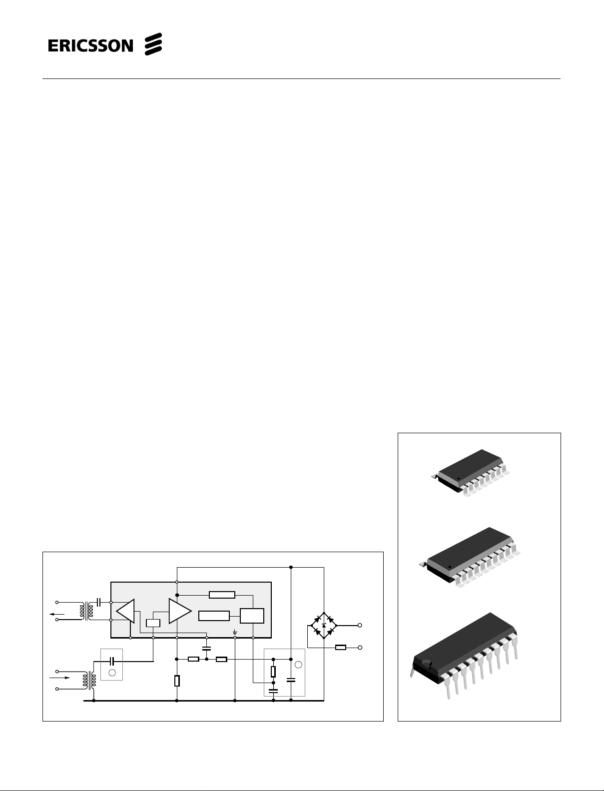
RECEIVE
TRANSMIT
18
17
2
Limiter
6
3
Figure 1. Functional diagram. DIP package.
1
Fast start - up
Reference
15
2
DC
supply
+
4
5,
14,16
1
Telephone
line
PBL38582
20-pin plastic SO
18-pin plastic DIP
1
PBL 385 82
Maximum Ratings
Parameter Symbol Min Max Unit
Line voltage, tp = 2 s V
Line current, continuous DIP I
Line current, continuous SO-20 package I
Line current, continuous SO-16 package I
Operating temperature range T
Storage temperature range T
No input should be set on higher level than pin 15.(+C)
R = 0-4kΩ
L
0 ohm when artificial
line is used
R
feed
+
E = 48.5V
5H+5H
= 400Ω+400Ω
ARTIFICIAL
C
600Ω
LINE
+
V
2
V
1
I
L
+ LINE
PBL 38582
V
L
with external
components
See fig. 4
L
L
L
PBL 38582/2 0 70 mA
L
Amb
Stg
Ω
310
Ω
350
Transmitter
V
3
input
V
018V
0 130 mA
0 100 mA
-40 +70 °C
-55 +125 °C
Receiver
output
4
C = 1µF when artificial line is used
470µF when no artificial line
R = 0 - 4 k
L
5H+5H
R
feed
+
E = 50.0V
= 400Ω+400Ω
Receiver
output
18
17
Transmitter
input
1µF
V
2
V
1
Uz= 15-16V
Ω
+
600Ω
PBL 38582
Limiter
6
R13
R14
- LINE
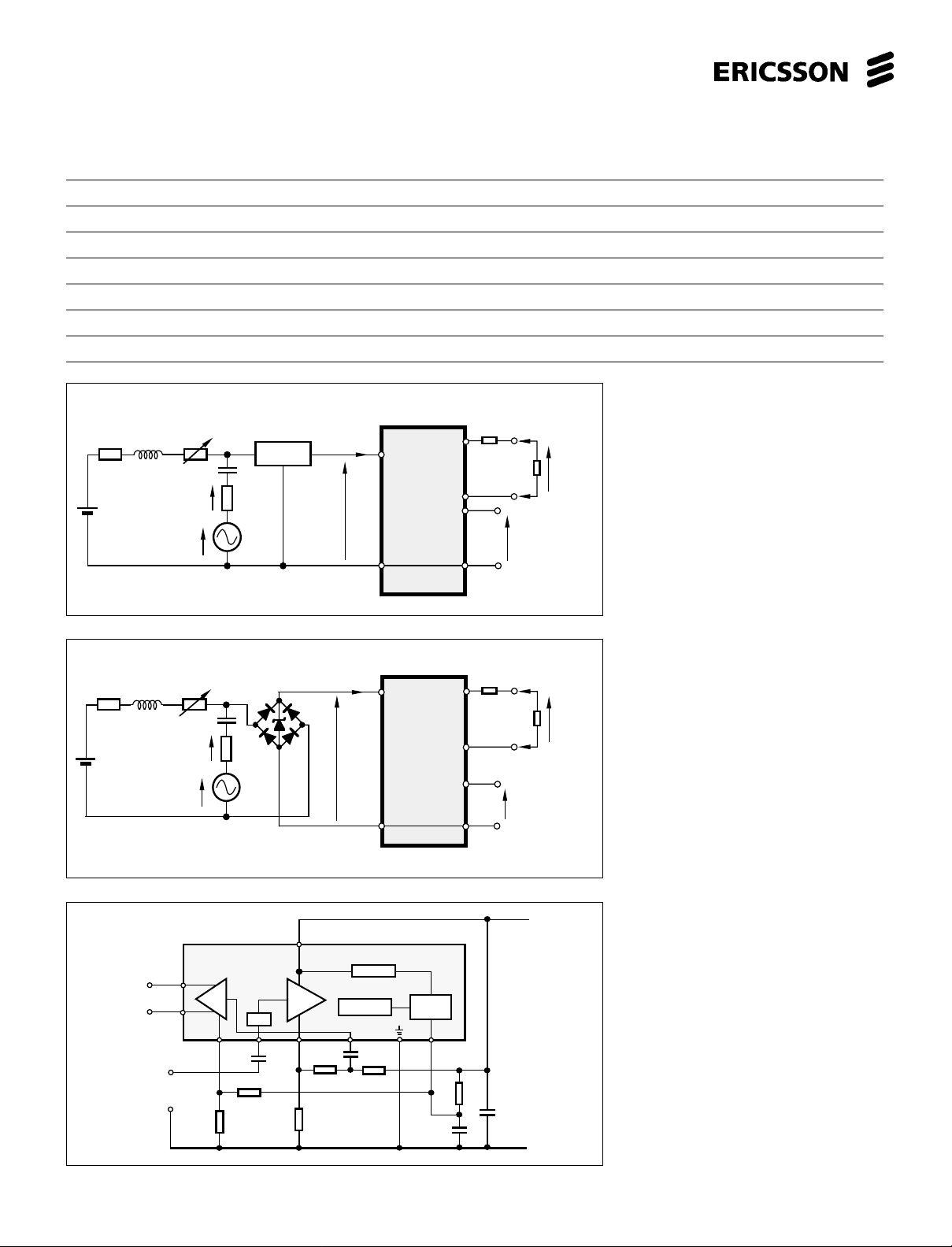
Figure 2. Test set up without
rectifier bridge
I
L
+ LINE
V
L
PBL 38582
with external
components
See fig. 4
- LINE
310
Ω
350
Ω
Transmitter
V
3
input
Receiver
V
output
4
.
Figure 3. Test set up with rectifier
bridge
.
1
Fast start - up
Reference
3
2
C3
R6
15
C4
R1
R2
DC
supply
+
4
14,16
5,
R3
C1
+Line
Figure 4. Circuit with external
components for test set up.
R1 = 6.2 k R2 = 62 k
R3 = 909
C2
-Line
R14 = 10k
C1 = 68 µF C2 = 15 nF
C3 = 0.1µF C4 = 47 nF
Ω
R6 = 75
Ω
DIP package pinning.
2
PBL 385 82
Electrical Characteristics
At T
= + 25° C. No cable and no line rectifier unless otherwise specified.
Amb
I
= 100 mA is not valid for 16-pin SO package.
L
Parameter Ref.fig. Conditions Min Typ Max Unit
Line voltage, VL 2 IL = 15 mA 3.3 3.7 4.1 V
2I
Transmitting gain 20 •10 log (V2 / V3); 1 kHz 24 25 26 dB
Transmitting frequency 2 200 Hz to 3.4 kHz -1 1 dB
response
Transmitter dynamic output 2 200 Hz - 3.4 kHz 1.5 V
Transmitter maximum output 2 200 Hz - 3.4 kHz 3 V
Transmitter output noise 2 Psof-weighting, Rel 1 V
Transmitter input impedance 2 1 kHz 13.5 17 20.5 kohm
pin 3
Receiving gain 20 • 10 log (V
Without gain regulation 2 R
Receiving gain 20 • 10 log (V
With gain regulation 2 R
2R
2R
Receiving range of regulation 2 1 kHz, RL = 0 to 900 ohm 3 5 7 dB
Receiving frequency response 2 200 Hz to 3.4 kHz -1 1 dB
Receiver output impedance 2 1 kHz, without 310Ω resistor 3 ohm
Receiver dynamic output 2 200 Hz - 3.4 kH 0.5 V
note 1 ≤ 2% distortion, IL = 20 - 100 mA
Receiver maximum output 3 Measured with line rectifier 0.9 V
Receiver output noise 2 A-weighting, Rel 1V
= 100 mA 11 13 15 V
L
≤ 2% distortion, IL = 20 - 100 mA
IL = 0 - 100 mA, V3 = 0 - 1 V
, RL = 0 -75 dB
rms
/ V1); 1 kHz
4
= 0 - xxx ohm, R11= 10k -18.5 -16.5 -14.5 dB
L
/ V1); 1 kHz, R11 not used
4
= 0 ohm, -18.5 -16.5 -14.5 dB
L
= 400 ohm -16 -14 -12 dB
L
= 900 ohm - 2.2 kohm -13.5 -11.5 -9.5 dB
L
200 Hz - 3.4 kHz,
IL = 0 - 100 mA, V1= 0 - 50 V
, with cable -85 dB
rms
0 - 5 km, Ø = 0.5 mm,
0 - 3 km, Ø = 0.3 mm
p
p
Psof
p
p
A
Notes:
1. The dynamic output can be nearly doubled if the 310Ω series resistor is omitted.
3

PBL 385 82
1
2
3
4
5
6
7
8
16
14
13
TO
+L
GR
-L
NA
NA
TI
+C
RI
-L
NA
NA
NA
9
12
10
11
-L
RE2
15
RE1
+L
1
18
RE 2
2
TO
3
TI
4
+C
5
-L
6
GR
7
NA
NA
8
NA
9 10
18-pin DIP
17
16
15
14
13
12
11
RE 1
-L
RI
-L
NA
NA
NA
NA
+L
TO
TI
+C
GR
NA
NA
NA
NA
1
2
3
4
-L
5
6
7
8
9
10
20
RE2
19
RE1
18
-L
17
RI
16
-L
15
NA
14
NA
13
NA
12
NA
11
NA
20-pin SO 16-pin SO
Figure 5. Pin configuration.
Pin Descriptions
Refer to figure 5.
DIP SO 20 SO 16 Name Function
1 1 1 +L Output of the transmitter amplifier. Connected to the line through a
polarity guard diode bridge.
2 2 2 TO Output of the transmitter amplifier. Connected through a resistor of 47 to 100 ohm to -L.
Sets the DC-charateristic of the circuit.The output has a low AC output impedance and
the signal is used to drive a side tone balancing network.
3 3 3 TI Input of transmit amplifier. Input impedance 17 k Ω ± 20 %.
4 4 4 +C The positive power supply terminal for most of the circuitry inside the PBL 385 82
(about 1 mA current consumption). The +C-pin is to be connected to a decoupling
capacitor of 47 µF to 150 µF.
6 6 6 GR The control input for the gain regulation in the receiver.
55 5
14 16 12 -L The negative power terminal, connected to the line through a polarity guard diode
16 18 14 bridge.
15 17 13 RI Input of the receive signal amplifier. Input impedance is 38 kohm ± 20 %.
17 19 15 RE2
18 20 16 RE1
77 7 NA
88 8 NA
99 9 NA
10 10 10 NA
11 11 11 NA
12 12 NA
13 13 NA
4
14 NA
15 NA
}
The receive signal amplifier outputs. Output impedance is approximately 3 ohm.
}

Functional description
1
2
+Line
R3
R6
PBL 38 582
+
3
C1
C2
-Line
Rs
≈1Ω
How to connect a
complex network.
Example:
a) b) c)
4
220Ω
820Ω
C
220Ω+820Ω//C
Design procedure; ref. to fig.4.
The design is made easier through that all
settable parameters are returned to ground (-line), this feature differs it from bridge
type solutions.To set the parameters in the
following order will result in that the
interaction between the same is minimized.
1. Set the circuit impedance to the line,
either 600Ω or complex. (R3 and C1). C1
should be big enough to give low
impedance compared with R3 in the
telephone speech frequency band.Too
large C1 will make the start-up slow. See
fig. 10.
2. Set the DC-characteristic that is
required in the PTT specification or in case
of a system telephone,in the PBX
specification (R6).There are also internal
circuit dependent requirements like supply
voltages etc.
3. Set the attac point where the line
length regulation ( if used ) is supposed to
cut in. Note that in some countries the line
length regulation is not allowed. In most
cases the end result is better and more
readily achieved by using the line length
regulation (line loss compensation) than
without.
4. Set the transmitter gain and
frequency response.
5. Set the receiver gain and frequency
response. See text how to limit the max.
swing.
6. Adjust the side tone balancing
network if used.The network in most cases
is just a coarse resistive divider to take
care of the first order of balancing. The fine
balancing is done by the DSP in the system.
7. Set the RFI suppression
components in case necessary.
8. Circuit protection. Apart from any
other protection devices used in the design a good practice is to connect a 15V
1W zener diode across the circuit , from
pin 1 to -Line.
Impedance to the line
The AC- impedance to the line is
set by R3, C1 and C2. Fig.6. The circuits
relatively high parallel impedance will not
influence the line impedance to any
noticeable extent.At low frequencies the
influence of C1 can not be neglected.
Series resistance of C1 that
Figure 6. AC-impedance.
is dependent on the temperature and the
quality of the component will cause some
of the line signal to enter pin 4. This
generates a closed loop in the transmitter
amplifier that in it´s turn will create an
active impedance thus lowering the
impedance to the line. The impedance at
high frequencies is set by C2 that also
acts as a RFI suppressor.
In many specifications the
impedance towards the line is specified as
a complex network. See fig. 6. In case a).
the error signal entering pin 4 is set by the
ratio ≈Rs/R3 (909Ω), where in case b). the
ratio at high frequencies will be Rs/220Ω
because the 820Ω resistor is bypassed by
a capacitor. To help up this situation the
complex network capacitor is connected
directly to ground, case c). making the ratio
Rs/220Ω+820Ω and thus lessening the
error signal. Conclusion: Connect like in
case c) when complex impedance is
specified.
DC - characteristic
The DC - characteristic that a
telephone set has to fulfill is mainly given
by the network administrator. Following
parameters are useful to know when the
DC behaviour of the telephone is to be set:
• The voltage of the feeding system
• The line feeding resistance 2 x.......
ohms.
• The maximum current from the line at
zero line length.
• The min. current at which the telephone
has to work (basic function).
PBL 385 82
• The lowest and highest voltage
permissible across the telephone set.
• The highest voltage that the
telephone may have at different line
currents. Normally set by the
network owners specification.The
lowest voltage for the telephone is
normally set by the voltages that are
needed for the different parts of the
telephone to function. For ex. for
transmitter output amplifier, receiver output amplifier, dialler, speech
switching. R6 will set the slope of the
DC-char. and the rest of the level is
set by some constants in the circuit
as shown in the equation below. The
slope of the DC-char. will also
influence the line length regulation
(when used ) and thus the gain of
both transmitter and receiver. See
the table under gain regulation. R6
also acts as power protection for the
circuit, this must be kept in mind
when low values of R6 are considered. See fig. 7.
V
Line
≈ 2+1. 5 ⋅R6 ⋅
V
telephoneline
≈1. 5V+
I
line
V
line
5

PBL 385 82
V
16
14
12
10
8
6
4
2
20 40 60 80 100 120
V telephone line
V line
V pin 4
V pin 2
I
L
mA
signal to the earphone and thus preventing
an acoustical shock. A resistor in series
with the output can very well be used to
increase the protection level. Note, that
the noise in the receiver is allways transmitter noise that has been more or less
well balanced out by the side tone network.
The RC - network (optional) at the
output is to stabilize against the inductive
load that an earphone represents.
PBL 38 582
+
+
Rx
-
17
(C)
18
The capacitor C is optional
Z
(C)
Z > 5k
Z
Figure 7. DC - characteristics.( R6 = 75Ω)
Transmitter amplifier
The transmitter amplifier in PBL38582
consists of three stages. The first stage is
an amplitude limiter for the input signal at
TI, in order to prevent the transmitted signal to exceed a certain set level and cause
distortion. The second stage amplifies
further the signal from the first and adds it
to a DC level from an internal DC-regulation
loop in order to give the required DC
characteristic to the telephone set. The
output of this stage is TO. The third stage
is a current generator that presents a high
impedance towards the line and has its
gain from TO to +L. The gain of this
amplifier is ZL/R6 where ZL is the
impedance across the telephone line.
Hence, the absolute maximum signal
amplitude that can be transmitted to the
line undistorted is dependent of R6.
(amplitude limiting)
The transmitter gain is set by the
analog (transmitter) signal from the passband circuit and the frequency response is
set by the capacitors at input circuit at pin
3, the low end being influenced by C3 and
the high end by C6. The input signal
source impedance to the transmitter
amplifier input TI should be reasonably low
in order to keep the gain spread down.
Receiver amplifier
The receiver amplifier consists of three
stages, the first stage being an input buffer
that renders the input a high impedance.
The second stage is a gain regulated differential amplifier and the third stage a
balanced power amplifier. The power
amplifier has a differential output with low
DC- offset voltage, therefore a series
capacitor with the load is normally not
necessary. The receiver amplifier uses at
max. swing 4-6 mA peak. This current is
drawn from the +Line. The gain and
frequency response is set at the input RI
with a RC-network. The receiver gain can
be regulated.The range of regulation from
the input to the output is 5 ± 2 dB (19 to
24dB). The balanced earphone amplifie
can not be loaded to full (both current and
signal level ) single ended.The signal would
be distorded when returned to ground.
A methode is shown in fig.8 how to
connect a light load (5k ac. or DC wise) to
the output. It is preferred that both outputs
are loaded the same. The receiver has, as
a principal protection, two series diodes
anti parallel across its output to limit the
Figure 8. Unbalanced Rx loading.
Gain regulation.
The receiver is gain regulated (line
loss compensated).
There is a fixed default compensation
on the chip that can be adjusted or or set to
constant high or low gain mode. The input
impedance at the gain regulation pin 6 is
5.5k ± 20%. The default regulation pattern
is valid when the input is left open. Fig. 9
shows a typical receiver gain pattern versus line length. The following will show,
what to alter, to change the look of the
curve.
a). Adjustable with R12 for the receiver.
b). The attack point of the regulatorcan be adjusted with resistors R13 or R14
to either direction, up or down, on the line
current axis.
c). The angle of elevation of the curve
is mainly set by the value of R6. If the DCcharacteristics is set according to the line
parameters and a correct value for R6 is
chosen the angle is mostly correct but it
can be adjusted with R6. The adjustement
will affect the DC-characteristics as well as
most of the other parameters. This is why
the DC- characteristic is set early in the
design phase.
6

Battery feed R13 R14 R6
Regulation:
48V, 2 • 200Ω ∞ ∞ 47Ω
48V, 2 • 400Ω ∞ ∞ 75Ω
48V, 2 • 800Ω ∞ 180k 100Ω
No regulation:
Set for low gain
All feedings ∞ <22k 47 - 100Ω
Set for high gain 18k ∞ 47Ω
Set for high gain 22k ∞ 75 - 100Ω
dB
c.
a.
b.
High limit
Low limit
Figure 9. Gain regulation principle.
PBL 385 82
I
L
What is balancing the side
tone?
where no balancing has been done is in
the order of 6 - 12 dB.
To understand that the side tone is
influenced by other factors like, the
To understand that side tone balancing
is to counteract the signal, that is
transmitted via the microphone and transmitter to the line, returning to the earphone
via the receiver.
That presence of a strong side tone
signal is disturbing in a way that one quite
instictively lowers ones own voice level
thus lowering the signal level for the other
party. But again, if the balance is too good
(seldom the case) the earphone will feel
”dead”. In practical terms what is expected
is the same amplitude of ones own voice
in the ear as when not talking in a telephone.
The need to lower the side tone level
a).
1
PBL 385 82
Tx Rx
2
b).
R6
c).
R8
R10
Zbal
}
R9
R7
C5
impedance of the line and the signal that
enters the ear acoustically directly from the
mouth and from the mouth through the
material in the handset. The signal that
enters the microphone from the earphone
acoustically will also influence the return
loss factor to the telephone line.
To understand that the side tone network
can be trimmed to form a veritable
”distortion analyser”, so that the distortion
that is present from the microphone, will be
the only signal entering the earphone and
this signal even being small will sound very
bad. It is better to induce some of the
fundamental frequency back by making
15
C4
R11
R12
Figure 10. The side tone suppression principle.
the balance less perfect at that frequency.
This is valid for a network that is trimmed to
only one frequency. It is to strive to trim the
network such that it will attenuate the fundamental and the harmonic frequencies
alike throughout the different line
combinations.
To understand that if one of the two
signals entering the balancing system
from either direction, direct from
microphone or via the line, is clipped, will
result in a very distorted signal entering the
receiver amplifier and thus the earphone.
Further , to remember that side tone is a
small signal that is the difference of two
large signals and that the amplitude of the
distortion can be up to ten times the
amplitude of the fundamental frequency.
A short guidance for under-
Telephone
set side
Line side
standing the side tone
principle. (See fig. 10.)
17
18
Z2
Z1
Assuming the line impedance to be 600Ω.
( theorethical value )
Z1 = Line impedance
Z2 = The telephone set impedance 600Ω
Z1//Z2 = 300Ω
R6 will have a certain value 39 - 100Ω to
give the telephone a specified DCcharacteristic and overcurrent protection.
Assuming that this DC-characteristic
requires R6=60Ω, hence it will be 1/5 of
the Z1//Z2. This will in transmitting mode
result that 1/5 of the ac-signal that is on the
line to appear across R6.
7

PBL 385 82
Note that the signals at points a. and b. are
180 degrees off phase.
10 x R6 ≈ R7 + Zbal Note #1
R7 ≈ Zbal Note#2
The ac-signal at point c. is now 1/10 of the
signal on the line because it is further
divided by two from point b. (R7≈Zbal).
Hence 10 x R1 ≈ R2 to satisfy the balancing
criteria. R12 is to set the receiver gain. (
can also be a volume control potentiometer).
Note #1 These values ensure that the
frequency behaviour of the transmitter is
not influenced. With the ratio 1/10 the
influence is 1 dB, and with ratio 1/20 it´s 0.5
dB.
Note #2 If the R7 is made low ohmic
compared with Zbal, it will load the latter
and result in a bad side tone
perfomannce, again if the R7 is made high
ohmic compared with Zbal will result in a
low signal to balance the side tone with and
make the balancing difficult. Making any of
the impedances unnecessary high will
make the circuit sensitive to RFI. All values
given here are approximate and serve as
starting entities only. The final trimming
of side tone network is a cut and try proposition because a part of the balance lies
in the acoustical path between the
microphone and earphone.
Start up circuit
The circuit contains a start up device
which function is to fast charge capacitor
C1 when the circuit goes into hook- off
condition. The fast charge circuit is a
thyristor function between pins 1 and 4 that
will stop conducting when the current
drainat pin 4 is lower than ≈ 700 µA + the
internal current consumption ( about 1
mA). Care must be taken when connecting
external load to pin 4 in order not to exeed
the ≈ 700 µA limit. Should this happen, it
would result in an inoperative speech
funktion. This circuit can not retrigger before
the voltage level at C1 drops below 2V or
the line voltage is below 1V. See fig. 10.
+Line
1
PBL 38 5 82
Tx
2
R6
DC supply
4
R3
C1
-Line
Figure 11. Fast startup function.
3
1
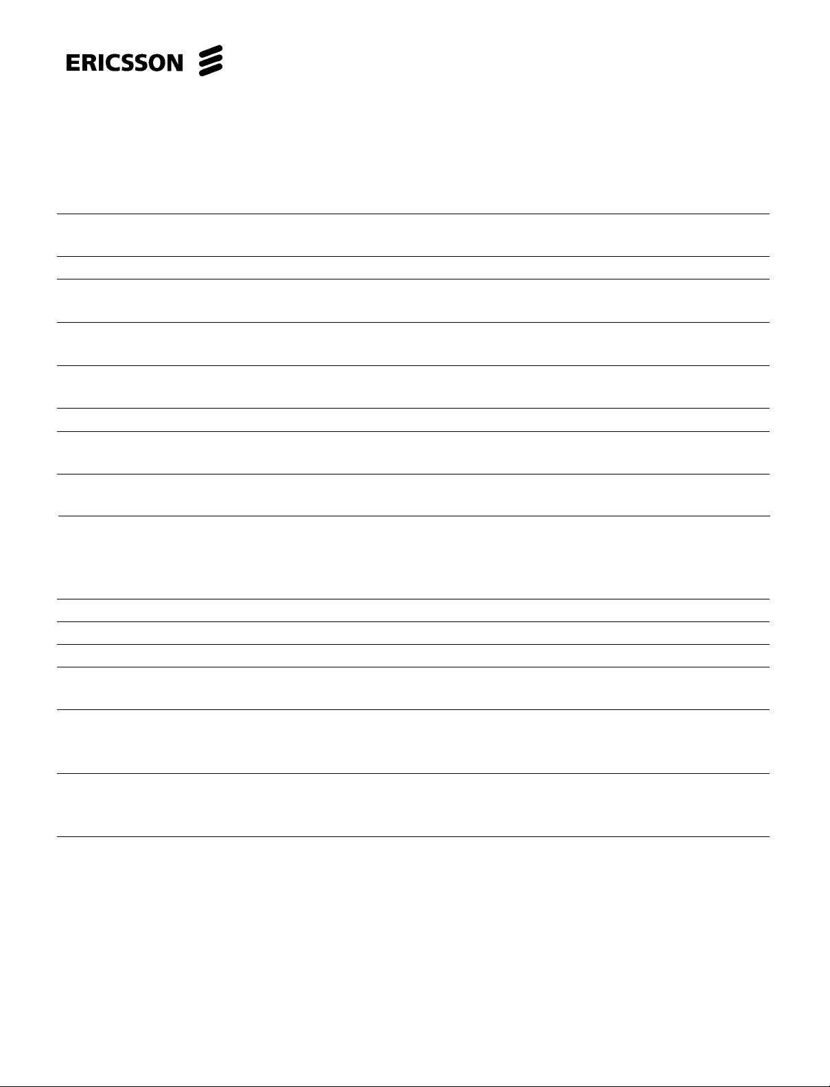
Fast start - up
RECEIVE
C7
1
mF
PBL 38582
18
Reference
6
R14
10k
Limiter
C6
3
2
15
C4 47nF
R1 6.2k R2 62k
R6
75W
>0.5W
TRANSMIT
2
2
C3
0.1mF
17
Figure 12. Typical insulated DECT-set line interface. DIP package.
5,
14,16
DC
supply
+
4
R3
910W
C1
68mF
1
C2 15nF
D1 D2
D5
D3 D4
Telephone
line
8

PBL 385 82
Ordering Information
Package Temp. Range Part No.
Plastic DIP -40 to +70°C PBL 385 82/1NS
Plastic SO20 -40 to +70°C PBL 385 82/1SOS
Plastic SO20 -40 to +70°C PBL 385 82/1SOT Tape & Reel
Plastic SO16 -40 to +70°C PBL 385 82/2SOS
Plastic SO16 -40 to +70°C PBL 385 82/2SOT Tape & Reel
Information given in this data sheet is believed to be
accurate and reliable. However no responsibility is
assumed for the consequences of its use nor for any
infringement of patents or other rights of third parties
which may result from its use. No license is granted
by implication or otherwise under any patent or patent
rights of Ericsson Components. These products are
sold only according to Ericsson Components' general
conditions of sale, unless otherwise confirmed in
writing.
Specifications subject to change without
notice.
IC4 (96087) B-Ue
© Ericsson Components AB
December 1999
Ordering number:
Ericsson Components AB
S-164 81 Kista-Stockholm, Sweden
Telephone: (08) 757 50 00
9
 Loading...