

Ericsson PBL38570-1N, PBL38570-1SO, PBL38570-1SOT Datasheet

PBL 385 70
Universal Speech Circuit
20-pin plastic SO
18-pin plastic DIP
September 1997
Figure 1. Functional diagram. DIP package.
1
Description.
PBL 38570 is a monolithic integrated speech transmission circuit for use in electronic
telephones. It is designed to accomodate either a low impedance dynamic or an electret
microphone. A separate input for DTMF dialling tones that is controlled by a mute signal,
and a signal summing point at the transmitter input, are available.
An internally preset line length compensation can be adjusted with external resistors
to fit into different current feed systems as for ex. 48 V, 2 x 200 ohms, 48 V, 2 x 400 ohms
and 48 V, 2 x 800 ohms. The line length compensation can be shut off in either high or
low gain mode. Application dependent parameters such as line balance, side tone level,
transmitter and receiver gains and frequency responces are set independently by
external components which means an easy adaption to various market needs.
The setting of the parameters if carried out in certain order will counteract the
interaction between the settings.
A number of different DC - supplies are provided to feed microphones and diallers.
Key features.
• Minimum number of external
components, 7 capacitors and 11
resistors.
• Easy adaption to various market
needs.
• Mute control input for operation with
DTMF - generator.
• A separate input for DTMF tones
controlled by mute.
• Transmitter and receiver gain
regulation for automatic loop loss
compensation.
• Extended current and voltage range
5 - 130 mA, down to 2 V.
• Differential microphone input for
good balance to ground.
• Balanced receiver output stage.
• Stabilized DC - supplies for low
current CMOS diallers and electret
microphones.
• 18 - pin DIP and 20 - pin SO packages.
• Short start up time.
• Excellent RFI performance.
PBL 38570
PBL 38570
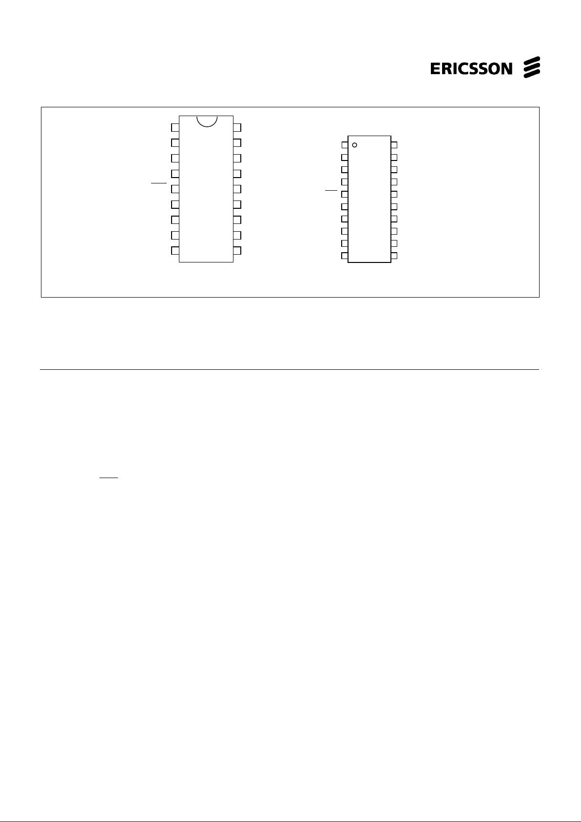
1. Line impedance and radio interference suppression.
2. Transmit gain and frequency response network.
3. Receive gain and frequency response network.
4. Side tone balance network.
5. DC-supply components.
17
14
2311
12
13
18
16
AM
AT
5
AR
15
4
+
10
AD
1
PBL 385 70
79
Sense input
DTMF
input
+
6
Mic.
8
DC-supply
+
Mute
(active low)
DC-output for
external devices
Telephone
line
5
2
4
3
1
Gain
regulation
PBL 385 70
2
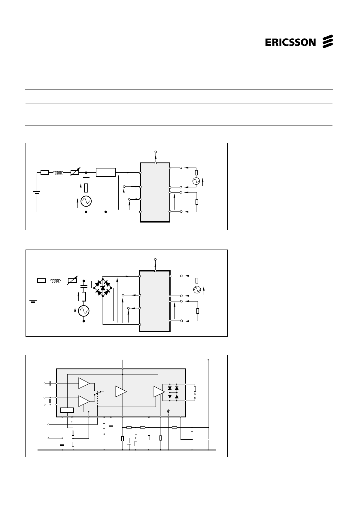
Figure 2. Test set up without rectifier
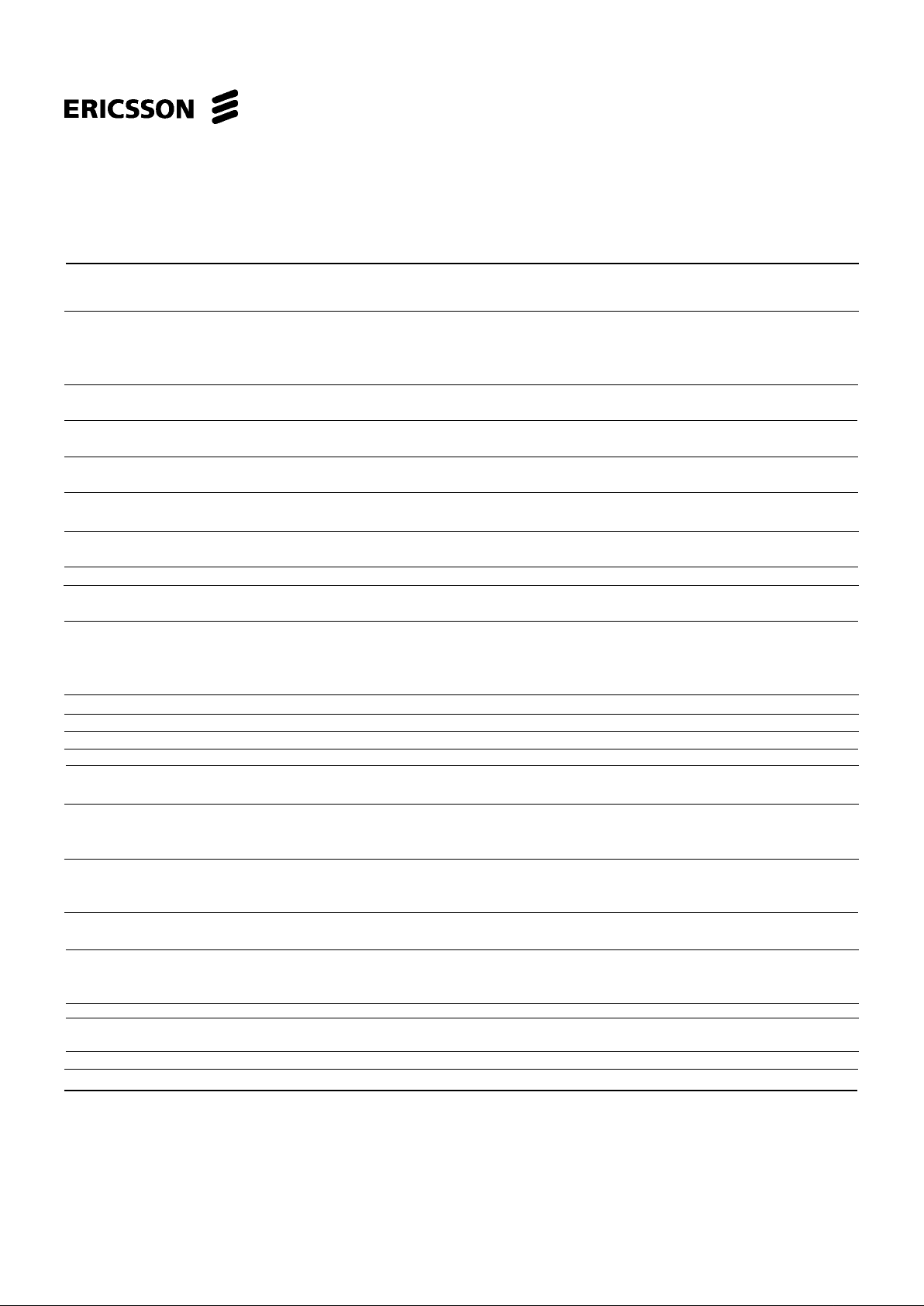
bridge.
Figure 3. Test set up with rectifier
bridge.
Figure 4. Circuit with external components for test set up.
* Not used in test set up.
18 pin DIP package.
Maximum Ratings
Parameter Symbol Min Max Unit
Line voltage, tp = 2 s V
L
018V
Line current, continuous DIP I
L
0 130 mA
Line current, continuous SO package I
L
0 100 mA
Operating temperature range T
Amb
-40 +70 °C
Storage temperature range T
Stg
-55 +125 °C
No input should be set on higher level than pin 4 (+C).
+
= 350Ω
+ LINE
- LINE
ARTIFICIAL
LINE
I
L
V
2
V
1
V
L
R = 0-4kΩ
L
0 ohm when artificial
line is used
MUTE
PBL 385 70
with external
components
See fig. 4
Z
Mic
= 350Ω
Z
Rec
MIC
REC
R
feed
= 400Ω+400Ω
600Ω
C
E = 48.5V
V
3
V
4
I
DC1
C = 1µF when artificial line is used
470µF when no artificial line
V
M
DC2
I
V
DC1
V
DC2
5H+5H
+
I
M
+
+ LINE
- LINE
I
L
V
2
V
1
V
L
R = 0 - 4kΩ
L
MUTE
PBL 385 70
with external
components
See fig. 4
Z
Mic
Z
Rec
MIC
REC
R
feed
= 400Ω+400Ω
600Ω
+
E = 50.0V
V
3
V
4
1µF
V
M
Uz= 15-16V
5H+5H
I
DC1
DC2
I
V
DC1
V
DC2
= 350Ω
= 350Ω
I
M
17
14
2311
12
13
18
16
AM
AT
5
AR
15
4
+
10
AD
1
PBL 385 70
79
Sense input
DTMF
input
+
6
Gain
regulation
Mic.
350Ω
8
DC-supply
+
Mute
(active low)
DC-output for
external devices
2.7k
47µF
*
*
18k
22k
100n
75Ω
910Ω
560Ω
11k
100n
6.2k
11k
10Ω
62k
47µF
15n
Rec.
350Ω
310Ω
220n
-Line
+Line
910Ω
47n
C1
C2
C3
C5
C6
C7
R1
R2
R4
R5
R6
R7
R8
R9
R10
R11
R12
R13
R3
R14
R16
C9
PBL 385 70
3
Electrical Characteristics
At T
Amb
= + 25° C. No cable and line rectifier unless otherwise specified.
Parameter fig. Conditions Min Typ Max Unit
Line voltage, V
L
2I
L
= 15 mA 3.3 3.7 4.1 V
2I
L
= 100 mA 11 13 15 V
Transmitting gain, note 1 20 •
10
log (V2 / V3); 1 kHz
2R
L
= 0 414345dB
2R
L
= 400 Ω 43.5 45.5 47.5 dB
2R
L
= 900 Ω - 2.2 kΩ 46 48 50 dB
Transmitting range of 2 1 kHz, R
L
= 0 to 900 Ω 357dB
regulation
Transmitting frequency 2 200 Hz to 3.4 kHz -1 1 dB
response
Transmitter input impedance 2 1 kHz 13.5 17 20.5 kΩ
pin 3
Transmitter dynamic output 2 200 Hz - 3.4 kHz 1.5 V
p
≤ 2% distortion, IL = 20 - 100 mA
Transmitter max output 2 200 Hz - 3.4 kHz 3 V
p
IL = 0 - 100 mA, V3 = 0 - 1 V
Transmitter output noise 2 Psoph-weighting, Rel 1 V
rms
, RL = 0 -75 dB
Psoph
Microphone input impedance 2 1 kHz 1.7(//2.7) kΩ
pin 12 (14),13 (15) note 3
Receiving gain, note 1 20 •
10
log (V4 / V1); 1 kHz
2R
L
= 0 Ω -18.5 -16.5 -14.5 dB
2R
L
= 400 Ω -16 -14 -12 dB
2R
L
= 900 Ω - 2.2 kΩ -13.5 -11.5 -9.5 dB
Receiving range of regulation 2 1 kHz, R
L
= 0 to 900 Ω 357dB
Receiving frequency response 2 200 Hz to 3.4 kHz -1 1 dB
Receiver input impedance 2 1kHz 30.4 38 45.6 kΩ
Receiver output impedance 2 1 kHz, 3(+310), note 3 Ω
Receiver dynamic output 2 200 Hz - 3.4 kHz 0.5 V
p
note 2 ≤ 2% distortion, IL = 20 - 100 mA
Receiver max output 3 Measured with line rectifier 0.9 V
p
200 Hz - 3.4 kHz, IL = 0 - 100 mA,
V
1
= 0 - 50 V
Receiver output noise 2 A-weighting, Rel 1V
rms
, with cable -85 dB
A
0 - 5 km, Ø = 0.5 mm, 0 - 3 km,
Ø = 0.4 mm
Mute input voltage 2 0.3 V
at mute (active low)
DC-supply voltage 2 I
L
= 20 - 100 mA
I
DC
= 0 mA 2.1 2.35 2.6 V
I
DC
= 2 mA 1.95 2.2 2.6 V
DC-supply current, pin 8. 2 2 mA
DC-output pin 8 input 4 VDC = 2.35 V 0.1 µA
leakage current (no supply)
DTMF transmitting gain 2 VM = 0.3 V, 1 kHz 24.5 26.5 28.5 dB
DTMF input impedance 2 1 kHz 20 25 30 kΩ
Notes
1. Adjustable to both higher and lower values with external components.
2. The dynamic output can be doubled, see applications information.
3. External resistor in the test set up.
Ref.
PBL 385 70
4
Figure 5. Pin configuration.
18-pin DIP
20-pin SO
}
}
+L
TO
TI
+C
Mute
GR
DCS
DCO
DR
RI
-L
MI 2
MI 1
MO
1
2
3
4
5
6
7
8
16
15
14
13
12
11
DCC DI
9 10
RE 2
RE 1
18
17
1
2
3
4
5
6
7
8
19
18
17
16
15
14
13
+L
TO
TI
+C
Mute
GR
DCS
DCO
RE 2
RE 1
DR
RI
-L
MI 2
MI 1
MO
9
12
10
11
DCC
NC
DI
NC
4
5
17
16
20
Pin Descriptions
Refer to figure 5.
DIP SO Name Function
1 1 +L Output of the DC-regulator and transmit amplifier, connected to the line through a polarity
guard diode bridge.
2 2 TO Output of the transmit amplifier, connected through a resistor of 47 to 100 ohm to -L,
sets the DC-characteristics of the circuit. The output has a low AC output impedance and the
signal is used to drive a side tone balancing network.
3 3 TI Input of transmit amplifier. Input impedance 17 kohm ± 20 %.
4 4 +C Positive power supply terminal for most of the circuitry inside the PBL 385 70 (about 1 mA current
consumption). The +C pin must be connected to a decoupling capacitor of 47 µF to 150 µF.
5 5 Mute When low, speech circuit is muted and the DTMF input is enabled. Maximum voltage (at mute) is
0.3 V, current sink requirement of external driver is min. 50 µA.
6 6 GR Control input for the gain regulation circuitry.
7 7 DCS Sense input to the DC-supply.
8 8 DC1 Output from the DC-supply.
9 9 DC2 Control of the DC-supply.
10 12 DI Input for the DTMF-signal. Input impedance is 25 kohm ± 20 %.
11 13 MO Output of the microphone amplifier or DTMF-amplifier.
12 14 MI 1
Inputs to the microphone amplifier. Input impedance 1.7 kohm ± 20 %.
13 15 MI 2
14 16 -L The negative power terminal, connected to the line through a polarity guard diode bridge.
15 17 RI Input of receiver amplifier. Input impedance is 38 kohm ± 20 %.
16 18 DR Control input for the receiver amplifier driving capacity.
17 19 RE 1
Receiver amplifier outputs. Output impedance is approximately 3 ohm.
18 20 RE 2
10 NC
11 NC
 Loading...