

Ericsson PBL38541-1N, PBL38541-1SO, PBL38541-1SOT Datasheet
1
PBL 385 41
PBL 385 41
Universal Speech Circuit
Description.
PBL 38541 is a monolithic integrated speech transmission circuit for use in
electronic telephones or in any other line interface application. High settable supply
current for auxiliary functions, up to 6.0 mA (at high line currents). The circuit is designed
to accomodate either a low impedance dynamic or an electret microphone. Microphone
can be muted separately. Payphone signaling and DTMF dialling tones have a separate
input that is controlled by a mute signal. A signal summing point is available at the
transmitter input. An internally preset line length compensation can be adjusted with
external resistors to fit into different current feed systems as for ex. 48 V, 2 x 200 ohms,
48 V, 2 x 400 ohms and 48 V, 2 x 800 ohms. The line length compensation can be shut
off in either high or low gain mode. Application dependent parameters such as line
balance, side tone level, transmitter and receiver gains and frequency responces are set
independently by external components which means an easy adaption to various market
needs. The setting of the parameters if carried out in certain order will counteract the
interaction between the settings. The circuit provides four different DC - supplies to feed
microphones,diallers and other more current consuming functions like handsfree systems.
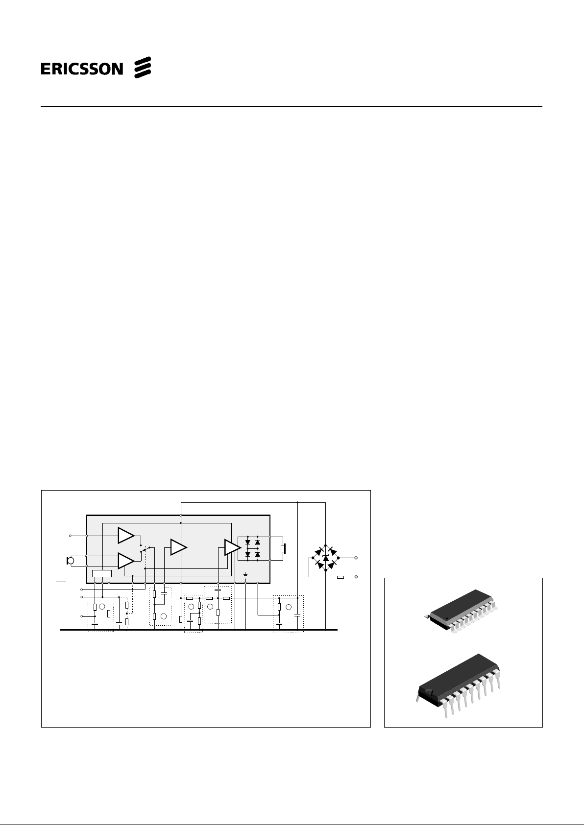
Pin numbers in this datasheet refer to 18-pin DIP package unless otherwhise noted.
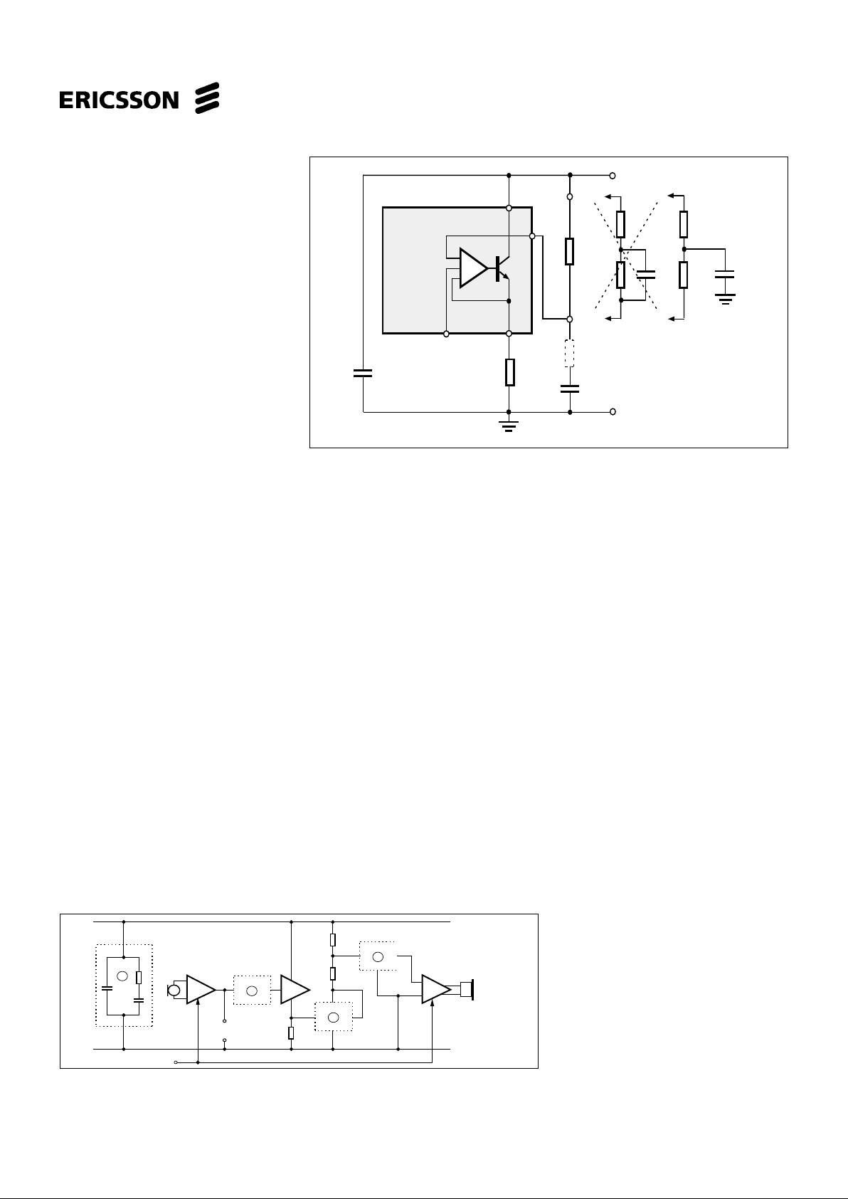
Figure 1. Functional diagram DIP package.
Key features.
• Minimum number of external
components, with two filtered DCsupplies, 7 capacitors and 11
resistors.
• Easy adaption to various market
needs.
• Mute control input for operation with
DTMF - generator.
• A separate signaling input for
payphone and DTMF tones controlled
by mute.
• Transmitter and receiver gain
regulation for automatic loop loss
compensation.
• Extended current and voltage range
4 - 130 mA, down to 2 .2V.
• Differential microphone input for good
balance to ground.
• Balanced receiver output stage.
• One stabilized DC - supply for low
current CMOS diallers and or electret
microphones. One settable current
limited supply with 6 mA max. current.
• Short start up time.
• Excellent RFI performance.
• 18 - pin DIP and 20 - pin SO packages.
17
14
2311
12
13
18
16
AM
AT
5
AR
15
4
+
10
AD
1
PBL 385 41
79
DTMF
input
+
6
Mic.
8
DC-supply
+
Mute
(active low)
DC2 - output for
external devices
Telephone
line
5
2
4
3
1
Gain
regulation
DC1
- output for
external devices
+
1. Impedance to the line and radio interference suppression
2. Transmitter gain and frequency responce network
3. Receiver gain and frequency responce network
4. Sidetone balance network
5. DC supply components
November 1998
20-pin plastic SO
PBL 385 41
PBL 385 41
18-pin plastic DIP
2
PBL 385 41
Figure 2. Test set up without rectifier
bridge.
Figure 3. Test set up with rectifier
bridge.
Figure 4. Circuit with external components for test set up. 2 x 400
Ω
48V.
* Not used in test set up.
DIP package pinning.
Maximum Ratings
Parameter Symbol Min Max Unit
Line voltage, tp = 2 s V
L
018V
Line current, continuous DIP I
L
0 130 mA
Line current, continuous SO package I
L
0 100 mA
Operating temperature range T
Amb
-40 +70 °C
Storage temperature range T
Stg
-55 +125 °C
No input should be set on higher level than pin 4 (+C).
+
= 350Ω
+ LINE
- LINE
ARTIFICIAL
LINE
I
L
V
2
V
1
V
L
R = 0-4kΩ
L
0 ohm when artificial
line is used
MUTE
PBL 385 41
with external
components
See fig. 4
Z
Mic
= 350Ω
Z
Rec
MIC
REC
R
feed
= 400Ω+400Ω
600Ω
C
E = 48.5V
V
3
V
4
I
DC1
C = 1µF when artificial line is used
470µF when no artificial line
V
M
DC2
I
V
DC1
V
DC2
5H+5H
+
I
M
+
+ LINE
- LINE
I
L
V
2
V
1
V
L
R = 0 - 4kΩ
L
MUTE
PBL 385 41
with external
components
See fig. 4
Z
Mic
Z
Rec
MIC
REC
R
feed
= 400Ω+400Ω
600Ω
+
E = 50.0V
V
3
V
4
1µF
V
M
Uz= 15-16V
5H+5H
I
DC1
DC2
I
V
DC1
V
DC2
= 350Ω
= 350Ω
I
M
17
14
2311
12
13
18
16
AM
AT
5
AR
15
4
+
10
AD
1
PBL 385 41
9
DTMF
input
+
6
Gain
regulation
Mic.
350Ω
8
DC-supply
+
Mute
(active low)
DC2 - output for
external devices
2.7k
*
18k
22k
100n
75Ω
910Ω
560Ω
11k
100n
6.2k
11k
10Ω
62k
47µF
15n
Rec.
350Ω
310Ω
220n
-Line
+Line
910Ω
47n
C1
C2
C3
C5
C6
47µF
C7
R1
*
R2a
R4
R5
R6
R7
R8
R9
R10
R11
R12
R13
R3
R14
R16
C9
+
47µF
C11
7
R17
DC1 - output for
external devices
>0.5W
4k
R2b
*
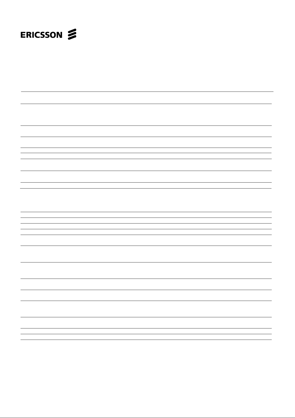
3
PBL 385 41
Electrical Characterisics
At T
Amb
= + 25° C. No cable and line rectifier unless otherwise specified.
Ref.
Parameter fig. Conditions Min Typ Max Unit
Line voltage, V
L
2I
L
= 15 mA 3.3 3.7 4.1 V
2I
L
= 100 mA 11 13 15 V
Transmitting gain, note 1 20 •
10
log (V2 / V3); 1 kHz
2R
L
= 0 41 43 45 dB
2R
L
= 400 Ω 43.5 45.5 47.5 dB
2R
L
= 900 Ω - 2.2 kΩ 46 48 50 dB
Transmitting range of 2 1 kHz, RL = 0 to 900 Ω 3 5 7 dB
regulation
Transmitting frequency 2 200 Hz to 3.4 kHz -1 1 dB
response
Transmitter input impedance, pin 3 2 1 kHz 13.5 17 20.5 kΩ
Microphone input impedance 2 1.7//(2.7) note 3 kΩ
Transmitter dynamic output 2 200 Hz - 3.4 kHz 1.5 V
p
≤ 2% distortion, IL = 20 - 100 mA
Transmitter max output 2 200 Hz - 3.4 kHz 3 V
p
IL = 0 - 100 mA, V3 = 0 - 1 V
Transmitter output noise 2 Psoph-weighting, Rel 1 V
rms
, RL = 0 -75 dB
Psoph
Receiving gain, note 1 20 • 10 log (V4 / V1); 1 kHz
2 R
L
= 0 Ω -18.5 -16.5 -14.5 dB
2 R
L
= 400 Ω -16 -14 -12 dB
2 RL = 900 Ω - 2.2 kΩ -13.5 -11.5 -9.5 dB
Receiving range of regulation 2 1 kHz, RL = 0 to 900 Ω 3 5 7 dB
Receiving frequency response 2 200 Hz to 3.4 kHz -1 1 dB
Receiver input impedance 2 1 kHz, 38 kΩ
Receiver output impedance 2 1 kHz, 3(+310)note 3 Ω
Receiver dynamic output 2 200 Hz - 3.4 kHz 0.5 V
p
note 2 ≤ 2% distortion, IL = 20 - 100 mA
Receiver max output 3 Measured with line rectifier 0.9 V
p
200 Hz - 3.4 kHz, IL = 0 - 100 mA,
V1= 0 - 50 V
Receiver output noise 2 A-weighting, Rel 1V
rms
, with cable -85 dB
A
0 - 3 km, Ø = 0.4 mm
0 - 5 km, Ø = 0.5 mm,
Mute input voltage 2 0.3 V
at mute (active low)
DC
1
-supply voltage 2 IL = 20 - 100 mA
Pin 9 R17 = 4k; I
DC1
=2 mA 3.4 3.7 4.0 V
DC2-supply voltage 2 IL = 20 - 100 mA
Pin 8 I
DC
= 0 mA 2.1 2.35 2.6 V
IDC = 2 mA 1.95 2.2 2.6 V
DC-output pin 8 input 4 VDC = 2.35 V 0.1 µA
leakage current (no supply)
DTMF transmitting gain 2 VM = 0.3 V, 1 kHz 24.5 26.5 28.5 dB
DTMF input impedance 2 1 kHz 20 25 30 kΩ
Notes
1. Adjustable to both higher and lower values with external components.
2. The dynamic output can be doubled, see applications information.
3. External resistor in the test set up.
4. The DC output voltage is reduced at low line voltage (see page 8).
4
PBL 385 41
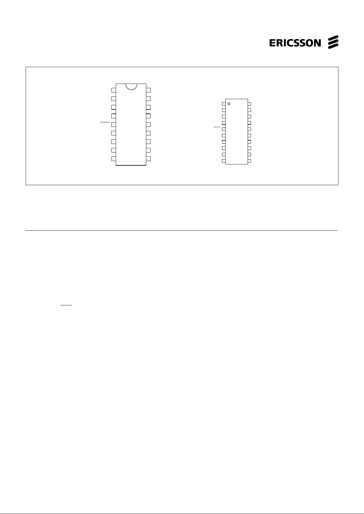
Figure 5. Pin configuration.
18-pin DIP
20-pin SO
Pin Descriptions
Refer to figure 5.
DIP SO Name Function
1 1 +L Output of the DC-regulator and transmitter amplifier, connected to the line through a polarity
guard diode bridge.
2 2 TO Output of the transmitter amplifier, connected through a resistor of 47 to 100 ohm to -L,
sets the DC-resistance of the circuit. The output has a low AC output impedance and the
signal is used to drive a side tone balancing network.
3 3 TI Input of the transmitter amplifier. Input impedance 17 kohm ± 20 %.
4 4 +C Positive power supply terminal for most of the circuitry inside the PBL 385 41 (about 1 mA current
consumption). The +C pin must be connected to a decoupling capacitor of 47 µF to 150 µF.
5 5 Mute When low, speech circuit is muted and the DTMF input is enabled. Maximum voltage (at mute) is
0.3 V, current sink requirement of external driver is 50 µA.
6 6 GR Control input for the gain regulation function.
7 7 DCS 1 Control input to the DC1-supply. A resistor to -line sets the maximum current load of the supply.
8 8 DCO 2 Output of the DC2-supply.
9 9 DCO 1 Output of the DC1-supply.
10 12 DI Input for the DTMF-signal. Input impedance 25 kohm ± 20 %.
11 13 MO Output of the microphone amplifier or DTMF-amplifier.
12 14 MI 1
Inputs to the microphone amplifier. Input impedance 1.7 kohm ± 20 %.
13 15 MI 2
14 16 -L The negative power terminal, connected to the line through a polarity guard diode bridge.
15 17 RI Input of receiver amplifier. Input impedance 38 kohm ± 20 %.
16 18 DR Control input for the receiver amplifier driving capability.
17 19 RE 1
Receiver amplifier outputs. Output impedance is approximately 3 ohm.
18 20 RE 2
10 Not connected
11 Not connected
+L
TO
TI
+C
Mute
GR
DCS
1
DCO
2
DR
RI
-L
MI 2
MI 1
MO
1
2
3
4
5
6
7
8
16
15
14
13
12
11
DCO
1
DI
9 10
RE 2
RE 1
18
17
1
2
3
4
5
6
7
8
19
18
17
16
15
14
13
+L
TO
TI
+C
Mute
GR
DCS
1
DCO
2
RE 2
RE 1
DR
RI
-L
MI 2
MI 1
MO
9
12
10
11
DCO
1
NC
DI
NC
4
5
17
16
20
}
}
5
PBL 385 41
1
2
+Line
R3
R6
PBL 385 41
+
3
C1
C2
-Line
Rs
≈1Ω
How to connect a
complex network.
220Ω+820Ω//Cx
Example:
a) b) c)
4
Cx
220Ω
820Ω
Figure 7. Block connections.
Figure 6. AC-impedance.
Functional description
Design procedure; ref. to fig.4.
The design is made easier through that all
settable parameters are returned to ground (-line), this feature differs it from bridge
type solutions.To set the parameters in the
following order will result in that the
interaction between the same is minimized.
1. Set the circuit impedance to the line,
either resistive (600Ω) or complex. (R3
and C1). C1 should be big enough to give
low impedance compared with R3 in the
telephone speech frequency band.Too
large C1 will make the start-up slow. See
fig. 6.
2. Set the DC-characteristic that is
required in the PTT specification or in case
of a system telephone,in the PBX
specification(R6). Observe the power
dissipated.There are also internal circuit
dependent requirements like supply voltages etc.
3. Set the attac point where the line
length regulation is supposed to cut in
(R1 and R2). Note that in some countries
the line length regulation is not allowed. In
most cases the end result isbetter and
more readily achieved by using the line
length regulation (line loss compensation)
than without. See fig. 13.
4. Set the transmitter gain and
frequency response.
5. Set the receiver gain and frequency
response. See text how to limit the max.
swing to the earphone.
6. Adjust the side tone balancing
network.
7. Set the RFI suppression
components in case necessary. In two
piece telephones the often ”helically”
wound cord acts as an aerial. The
microphone input with its high gain is
especially sensitive.
8. Circuit protection. Apart from any
other protection devices used in the design a good practice is to connect a 15V
1W zener diode across the circuit , from
pin 1 to -Line.
Impedance to the line
The AC- impedance to the line is
set by R3, C1 and C2. Fig.6. The circuits
relatively high parallel impedance will not
influence it to any noticeable extent. At low
frequencies the influence of C1 can not be
neglected. Series resistance of C1 that is
dependent on the temperature and the
quality of the component will cause some
of the line signal to enter pin 4. This
generates a closed loop in the transmitter
amplifier that in it´s turn will create an
active impedance thus lowering the
impedance to the line. The impedance at
high frequencies is set by C2 that also
acts as a RFI suppressor.
In many specifications the
impedance towards the line is specified as
a complex network. See fig. 6. In case a).
the error signal entering pin 4 is set by the
ratio ≈Rs/R3 (910Ω), where in case b). the
ratio at high frequencies will be Rs/220Ω
because the 820Ω resistor is bypassed by
a capacitor. To help up this situation the
complex network capacitor is connected
directly to ground, case c). making the ratio
Rs/220Ω+820Ω and thus lessening the
error signal. Conclusion: Connect like in
case c) when complex impedance is
specified.
DC - characteristic
The DC - characteristic that a
telephone set has to fulfill is mainly given
by the network administrator. Following
parameters are useful to know when the
DC behaviour of the telephone is to be set:
• The voltage of the feeding system
• The line feeding resistance 2 x.......
ohms.
• The maximum current from the line at
zero line length.
• The min. current at which the
telephone has to work (basic
function).
• The lowest and highest voltage
permissible across the telephone set.
• The highest voltage that the telephone
may have at different line currents.
Normally set by the network owners
specification.The lowest voltage for the
telephone is normally set by the voltages that are needed for the different
parts of the telephone to function. For
ex. for transmitter output amplifier,
receiver output amplifier, dialler,
speech switching and loudspeaker
amplifier in a handsfree telephone etc.
+
1
AM AT
AR
2
Transmitter summing
input
Mute
+ Line
- Line
3
4
 Loading...