February 1999
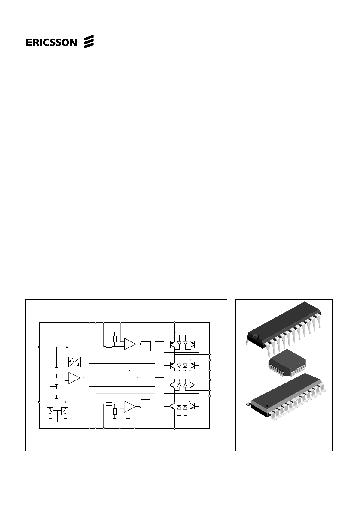
28-pin PLCC package
22-pin plastic DIP package
24-pin SO package
Key Features
• Dual chopper driver in a single
package.
• Operation down to -40°C.
• 750 mA continuous output current
per channel.
• Low power dissipation, 2.0 W at
2 x 500 mA output current.
• Close matching between channels
for high microstepping accuracy.
• Digital filter on chip eliminates
external filtering components.
• Plastic 22-pin batwing DIL package,
24-pin SOIC batwing or 28-pin power
PLCC. All with lead-frame for
heatsinking through PC board
copper.
PBL 3775/1
Dual Stepper Motor Driver
Description
The PBL 3775/1 is a switch-mode (chopper), constant-current driver IC with two
channels, one for each winding of a two-phase stepper motor. The circuit is similar to
Ericsson´s PBL 3773/1. While several of Ericsson´s dual stepper motor drivers are
optimized for micro-stepping applications, PBL 3775/1 is equipped with a disable
input to simplify half-stepping operation.
The PBL 3775/1 contains a clock oscillator, which is common for both driver
channels, a set of comparators and flip-flops implementing the switching control, and
two output H-bridges, including recirculation diodes.
Voltage supply requirements are + 5 V for logic and + 10 to + 45 V for the motor.
The close match between the two driver channels guarantees consistent output
current ratios and motor positioning accuracy.
PBL3775/1
PBL
3775/1
RC
PBL 3775/1
M
A1
M
B1
M
B2
M
A2
GNDC
2
V
R2
Phase
2
V
CC
C
1
V
R1
Phase
1
E
1
E
2
V
CC
SRQ
Logic
S
R
Q
+
–
Logic
+
–
V
MM2
V
MM1
Dis
1
Dis
2
+
–
Figure 1. Block diagram
PBL 3775/1

PBL 3775/1
2
Maximum Ratings
Parameter Pin No. (DIP) Symbol Min Max Unit
Voltage
Logic supply 12 V
CC
07V
Motor supply 4, 19 V
MM
045V
Logic inputs 9, 10, 13, 14 V
I
-0.3 6 V
Analog inputs 7, 8, 15, 16 V
A
-0.3 V
CC
V
Current
Motor output current 1, 3, 20, 22 I
M
-850 +850 mA
Logic inputs 9, 10, 13, 14 I
I
-10 mA
Analog inputs 7, 8, 15, 16 I
A
-10 mA
Temperature
Operating junction temperature T
J
-40 +150 °C
Storage temperature T
S
-55 +150 °C
Power Dissipation (Package Data)
Power dissipation at T
BW
= +25°C, DIP and PLCC package P
D
5W
Power dissipation at T
BW
= +125°C, DIP package P
D
2.2 W
Power dissipation at T
BW
= +125°C, PLCC package P
D
2.6 W
Recommended Operating Conditions
Parameter Symbol Min Typ Max Unit
Logic supply voltage V
CC
4.75 5 5.25 V
Motor supply voltage V
MM
10 40 V
Output emitter voltage V
E
1.0 V
Motor output current I
M
-750 +750 mA
Operating junction temperature T
J
-20 +125 °C
Rise and fall time logic inputs t
r,
, t
f
2 µs
Oscillator timing resistor R
T
2 12 20 kohm
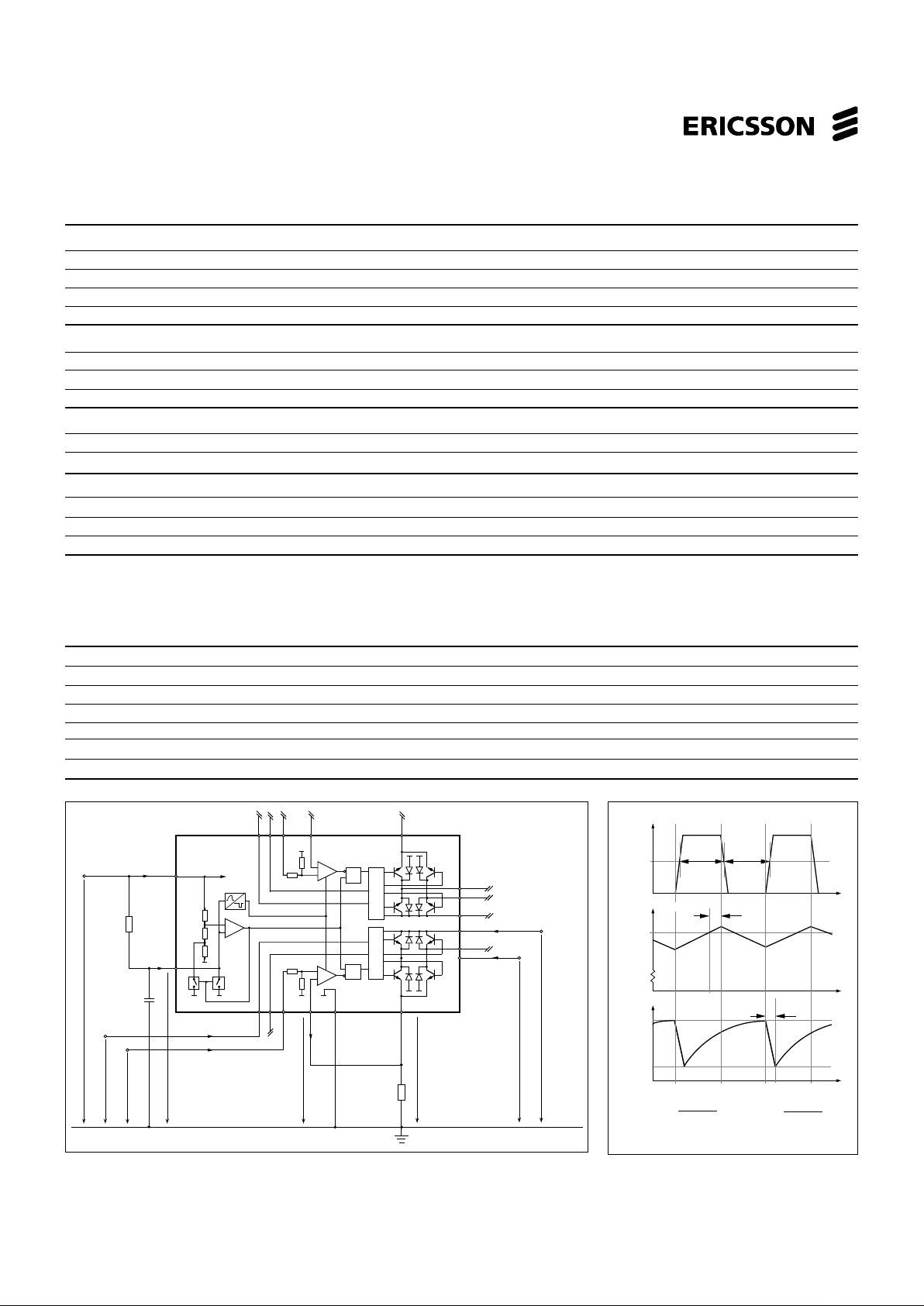
Figure 3. Definition of terms.
Figure 2. Definition of symbols.
V
R
t
d
t
50 %
t
on
t
off
| V – V |
MA MB
t
t
V
RC
t
b
V ( I )
E
M
f =
s
t
ontoff
+
1
D =
t
t
on
off
+
t
on
I I
M OL
I
CC
I I I
I IH IL
I
A
4 700 pF
V
CC
V
V
V
I
IH
IL
V
V
A
R
V
V
V
CH
C
A
I
I
C
A
V
E
V
MM
R
S
R
T
12 kW
I
MM
C
T
I
R
V
RC
I
RC
V
MA
V
M
RC
PBL 3775/1
19
11
12
M
A1
M
B1
M
B2
M
A2
GNDC2V
R2
Phase
2
V
CC
C
1VR1
Phase
1
E
1
E
2
V
CC
22
20
14
15
SRQ
16
5, 6, 17, 18
Logic
21
S
R
Q
+
–
Logic
+
–
4
1
3
2
87
9
V
MM2
V
MM1
Dis
1
10
Dis
13
2
+
–

PBL 3775/1
3
Electrical Characteristics
Electrical characteristics over recommended operating conditions, unless otherwise noted. - 20° C ≤ Tj ≤ + 125° C.
Ref.
Parameter Symbol fig. Conditions Min Typ Max Unit
General
Supply current I
CC
2 Note 4. 55 70 mA
Supply current I
CC
2 Dis1= Dis2= HIGH. 7 10 mA
Total power dissipation P
D
8VMM= 24 V, IM1= IM2= 500 mA. 2.0 2.3 W
Notes 2, 3, 4.
Total power dissipation P
D
8VMM= 24 V, IM1= 700 mA, IM2= 0 mA. 1.7 2.0 W
Notes 2, 3, 4.
Thermal shutdown junction temperature 160 °C
Turn-off delay t
d
3TA = +25°C, dVC/dt ≥ 50 mV/µs, 1.1 2.0 µs
I
M
= 100 mA. Note 3.
Logic Inputs
Logic HIGH input voltage V
IH
2 2.0 V
Logic LOW input voltage V
IL
2 0.6 V
Logic HIGH input current I
IH
2VI = 2.4 V 20 µA
Logic LOW input current I
IL
2VI = 0.4 V -0.2 -0.1 mA
Analog Inputs
Threshold voltage V
CH
2VR=5 V 480 500 520 mV
Input current I
A
2VR= 5 V 500 µA
|V
C1—VC2
| mismatch V
Cdiff
21mV
Motor Outputs
Lower transistor saturation voltage 10 I
M
= 500 mA 0.4 0.8 V
Lower transistor leakage current 2 V
MM
=41 V,TA = +25°C. Dis1= Dis2= HIGH. 100 µA
Lower diode forward voltage drop 11 I
M
= 500 mA 1.1 1.3 V
Upper transistor saturation voltage 12 I
M
= 500 mA. 1.1 1.4 V
Upper diode forward voltage drop 13 I
M
= 500 mA. 1.1 1.4 V
Upper transistor leakage current 2 V
MM
=41 V,TA = +25°C. Dis1= Dis2= HIGH.
.
100 µA
Chopper Oscillator
Chopping frequency f
s
3CT = 4 700 pF, RT = 12 kohm 21.5 23.0 24.5 kHz
Digital filter blanking time t
b
3CT = 4 700 pF. Note 3. 1.0 µs
Thermal Characteristics
Ref.
Parameter Symbol fig. Conditions Min Typ Max Unit
Thermal resistance Rth
J-BW
DIL package. 11 °C/W
Rth
J-A
14 DIL package. Note 2. 40 °C/W
Rth
J-BW
PLCC package. 9 °C/W
Rth
J-A
14 PLCC package. Note 2. 35 °C/W
Rth
j-c
SO package 13 °C/W
Rth
j-a
SO package 42 °C/W
Notes
1. All voltages are with respect to ground. Currents are positive into, negative out of specified terminal.
2. All ground pins soldered onto a 20 cm
2
PCB copper area with free air convection, T
A
= + 25° C.
3. Not covered by final test program.
4. Switching duty cycle D = 30 %, f
s
= 23.0 kHz.
