

February 1999
PBL 3771/1
PBL 3771/1
Precision Stepper Motor Driver
Description
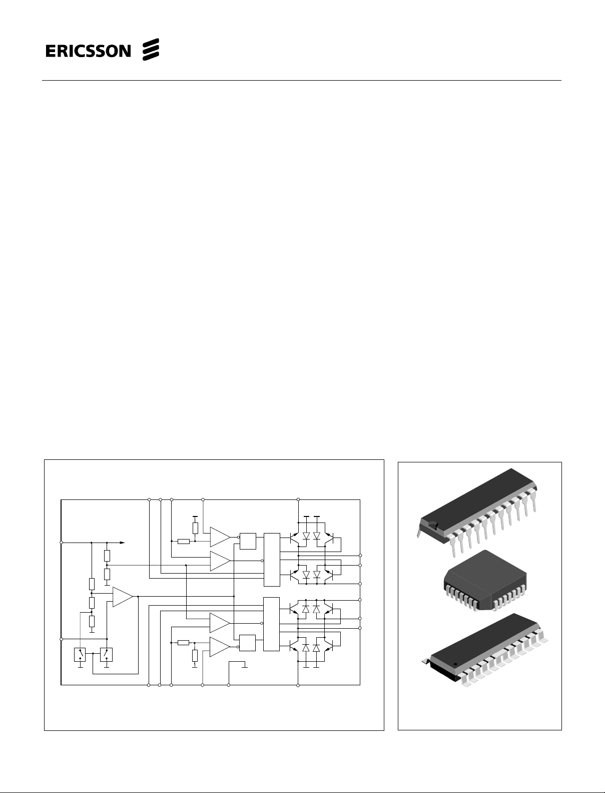
The PBL 3771/1 is a switch-mode, constant-current driver IC (chopper) with two
channels, one for each winding of a two-phase stepper motor. The circuit is especially
developed for use in microstepping applications in conjunction with the matching dual
DAC (Digital-to-Analog Converter) PBM 3960. A complete driver system consists of
these two ICs, a few passive components and a microprocessor for generation of the
proper control and data codes required for microstepping.
The PBL 3771/1 contains a clock oscillator, which is common for both driver
channels; a set of comparators and flip-flops implementing the switching control; and
two H-bridges with internal recirculation diodes. Voltage supply requirements are +5 V
for logic and +10 to +45 V for the motor. Maximum output current is 650 mA per
channel.
A special logic function is used to select slow or fast current decay in the output
stage for improved high-speed microstepping.
The close match between the two driver channels guarantees consistent output
current ratios and motor positioning accuracy.
Key Features
• Dual chopper driver in a single
package.
• 650 mA output current per channel.
• Close matching between channels for
high microstepping accuracy.
• Selectable slow/fast current decay for
improved high-speed microstepping.
• Improved low-level linearity.
• Specially matched to Dual DAC
PBM 3960.
• Selection of packages, 22-pin
“batwing” DIP, 24 pin "batwing" SOIC
or 28-lead PLCC with lead-frame for
heat-sinking through PC board
copper.
PBL 3771/1
V
CC
RC
V
CC
+
–
Figure 1. Block diagram.
Phase
Phase
VR1CD
1
1
C
1
–
+
+
–
–
+
+
–
R
S
SRQ
Q
Logic
Logic
E
1
M
A1
M
B1
V
MM1
V
MM2
M
B2
M
A2
PBL
3771/1
PBL 3771/1
VR2CD
2
2
GNDC
2
E
2
28-pin PLCC package
22-pin plastic DIP package
24-pin SO package
1
PBL 3771/1
50 %
V
CH
t
on
t
off
V
E
| V – V |
MA MB
t
d
t
t
f =
s
tont
off
+
D =
t
t
on
off
+
1
t
on
Maximum Ratings
Parameter Pin no. (DIL) Symbol Min Max Unit
Voltage
Logic supply 11 V
Motor supply 3, 20 V
Logic inputs 7, 8, 15, 16 V
Comparator inputs 10, 13 V
Reference inputs 9, 14 V
Current
Motor output current 1, 4, 19, 22 I
Logic inputs 7, 8, 15, 16 I
Analog inputs 10, 13 I
Oscillator charging current 12 I
Temperature
Operating junction temperature T
Storage temperature** T
** Circuit only. The packaging can handle max 60°C
Recommended Operating Conditions
CC
MM
I
C
R
M
I
A
RC
J
S
07V
045V
-0.3 6 V
-0.3 V
CC
V
-0.3 7.5 V
-700 +700 mA
-10 mA
-10 mA
5mA
-40 +150 °C
-55 +150 °C
Parameter Symbol Min Typ Max Unit
Logic supply voltage V
Motor supply voltage V
Motor output current *** I
Junction temperature **** T
Rise time logic inputs t
Fall time logic inputs t
Oscillator timing resistor R
*** In microstepping mode, “sine/cosine” drive where I
= 650 • cos(θ) and I2 = 650 • sin(θ) mA, otherwise 500 mA/channel both
1
CC
MM
M
J
r
f
T
4.75 5 5.25 V
10 40 V
-650 650 mA
-20 +125 °C
2 µs
2 µs
2 15 20 kohms
channels fully on.
****See operating temperature chapter.
4
1
3
20
22
19
Pin numbers refer to
DIL-package
M
A1
M
B1
V
MM1
V
MM2
M
B2
I I
M OL
M
A2
I
MM
V
V
MM
M
V
MA
Phase
1
PBL 3771/1
V
I
CC
CC
11
15 kW
R
T
I
RC
RC
12
3 300 pF
V
CC
C
T
I I I
I IH IL
V
I
V
IH
V
V
IL
V
I
A
A
R
7
V
CC
+
–
16
Phase
2
15 14
1
1
10
98
–
R
+
S
+
–
–
+
SRQ
+
–
5, 6, 17, 18
13
VR2CD
2
GNDC
2
I
C
I
A
820 pF
C
1 kW
C
V
CH
V
C
C
VR1CD
E
1
2
Q
Logic
Logic
21
E
2
R
C
V
E
R
S
Figure 2. Definitions of symbols.
2
Figure 3. Definition of terms.
PBL 3771/1
Electrical Characteristics
Electrical characteristics over recommended operating conditions, unless otherwise noted. -20°C - TJ - +125°C.
Parameter Symbol fig. Conditions Min Typ Max Unit
General
Supply current I
Total power dissipation P
Turn-off delay t
Logic Inputs
Logic HIGH input voltage V
Logic LOW input voltage V
Logic HIGH input current I
Logic LOW input current I
Reference Inputs
Input resistance R
Input current I
Turn-off voltage V
Comparator Inputs
Threshold voltage V
| V
- V
CH1
| mismatch V
CH2
Input current I
Motor Outputs
Lower transistor saturation voltage I
Lower transistor leakage current V
Lower diode forward voltage drop I
Upper transistor saturation voltage I
Upper transistor leakage current V
Upper diode forward voltage drop I
Chopper Oscillator
Chopping frequency f
Ref.
CC
D
VMM = 40 V, IM1= 450 mA, IM2= 0 mA. 1.4 1.6 W
38 50 mA
Notes 2, 3.
V
= 40 V, IM1 = IM2 = 318 mA. 1.6 1.8 W
MM
Notes 2, 3.
3Ta = +25°C, dVC/dt ≥ 50 mV/µs. 1.0 1.5 µs
d
Note 3.
IH
IL
IH
IL
R
R
TO
CH
CH,diff
C
s
VI = 2.4 V 20 µA
VI = 0.4 V -0.4 mA
Ta = +25°C 5 kohms
Ta = +25°C, VR = 2.5 V. 0.5 1.0 mA
RC = 1 kohms, VR = 2.5 V 430 450 470 mV
RC = 1 kohms 1 mV
= 500 mA 1.00 1.20 V
M
= 41 V, VE = VR = 0 V, VC = V
MM
= 500 mA 1.10 1.25 V
M
= 500 mA 1.20 1.35 V
M
= 41 V, VE = VR = 0 V, VC = V
MM
= 500 mA 1.00 1.25 V
M
3CT = 3300 pF, RT = 15 kohms 25.0 26.5 28.0 kHz
2.0 V
20 29 38 mV
-10 1 µA
CC
CC
0.8 V
300 µA
300 µA
Thermal Characteristics
Parameter Symbol fig. Conditions Min Typ Max Unit
Thermal resistance Rth
Notes
1. All voltages are with respect to ground. Currents are positive into, negative out of specified terminal.
2. All ground pins soldered onto a 20 cm
3. Not covered by final test program.
4. Switching duty cycle D = 30%, f
Ref.
13 DIL package. 11 °C/W
J-BW
Rth
13 DIL package. Note 2. 40 °C/W
J-A
Rth
13 PLCC package. 9 °C/W
J-BW
Rth
13 PLCC package. Note 2. 35 °C/W
J-A
Rth
13 SO package. 13 °C/W
J-BW
Rth
13 SO package. Note 2. 42 °C/W
J-A
2
PCB copper area with free air convection.
= 26.5 kHz.
S
3
 Loading...