

Ericsson KRD 103 117/1, KRD 103 117/3 Maintenance Manual

ericssonz
Maintenance Manual
NPC-200
Portable Radio
KRD 103 117/1 (VHF)
KRD 103 117/3 (UHF)
Ericsson Inc.
Private Radio Systems
Mountain Vie w Road
Lynchburg, Virginia 24502
AE/LZB 119 1658 R1A
1-800-528-7711 (Outside US A , 804-528-7711) Printed in U.S.A.
Copyright© March 1996, Ericsson Inc.
TABLE OF CONTENTS
Page
SPECIFICATIONS . . . . . . . . . . . . . . . . . . . . . . . . . . . . . . . . . . . . . . . . . . . . . . . . . . 2
GENERAL . . . . . . . . . . . . . . . . . . . . . . . . . . . . . . . . . . . . . . . . . . . . . . . . . . . . . . . 2
CIRCUIT DESCRIPTION . . . . . . . . . . . . . . . . . . . . . . . . . . . . . . . . . . . . . . . . . . . . . . 2
SYNTHESIZING . . . . . . . . . . . . . . . . . . . . . . . . . . . . . . . . . . . . . . . . . . . . . . . . 3
RECEIVER . . . . . . . . . . . . . . . . . . . . . . . . . . . . . . . . . . . . . . . . . . . . . . . . . . . 3
Antenna Switch F401 . . . . . . . . . . . . . . . . . . . . . . . . . . . . . . . . . . . . . . . . . 3
First RF Amplifier (Q101) . . . . . . . . . . . . . . . . . . . . . . . . . . . . . . . . . . . . . . . 3
First Mixer (D101) . . . . . . . . . . . . . . . . . . . . . . . . . . . . . . . . . . . . . . . . . . . 3
First IF Pre-Amplifier (Q2) . . . . . . . . . . . . . . . . . . . . . . . . . . . . . . . . . . . . . . 4
IF IC (IC1) . . . . . . . . . . . . . . . . . . . . . . . . . . . . . . . . . . . . . . . . . . . . . . . 4
Squelch Circuit (IC1) . . . . . . . . . . . . . . . . . . . . . . . . . . . . . . . . . . . . . . . . . 4
TRANSMITTER . . . . . . . . . . . . . . . . . . . . . . . . . . . . . . . . . . . . . . . . . . . . . . . . 4
Microphone Amplifier (Q701) . . . . . . . . . . . . . . . . . . . . . . . . . . . . . . . . . . . . . 4
High Pass Filter/Pre-Emphasis/Limiter Amplif ier . . . . . . . . . . . . . . . . . . . . . . . . . . . 4
MIC Mute (Q702 And Q703) . . . . . . . . . . . . . . . . . . . . . . . . . . . . . . . . . . . . . 4
Low Pass Filter (IC703) . . . . . . . . . . . . . . . . . . . . . . . . . . . . . . . . . . . . . . . . 4
TX Pre-Amplifier (Q508) . . . . . . . . . . . . . . . . . . . . . . . . . . . . . . . . . . . . . . . 4
Power Module And Power Controller (IC501, L401, D401, Q501, Q506 And Q507) . . . . . . . . 4
Transmit Inhibit (Q502 And Q503) . . . . . . . . . . . . . . . . . . . . . . . . . . . . . . . . . . 4
Antenna Switch (D402 And D403) . . . . . . . . . . . . . . . . . . . . . . . . . . . . . . . . . . 4
TABLE OF CONTENTS - Cont.
Page
REGULATORS . . . . . . . . . . . . . . . . . . . . . . . . . . . . . . . . . . . . . . . . . . . . . . . . . 5
LOGIC SECTION . . . . . . . . . . . . . . . . . . . . . . . . . . . . . . . . . . . . . . . . . . . . . . . 5
Microprocessor (IC601) . . . . . . . . . . . . . . . . . . . . . . . . . . . . . . . . . . . . . . . 5
EEPROM (IC604) . . . . . . . . . . . . . . . . . . . . . . . . . . . . . . . . . . . . . . . . . . 5
Receive Tone Decoder (IC705 , IC 60 2 And Q601) . . . . . . . . . . . . . . . . . . . . . . . . . . 5
2-Tone Decode r . . . . . . . . . . . . . . . . . . . . . . . . . . . . . . . . . . . . . . . . . . . . 5
Transmit CTCSS Tone Or DCSS Encoder (IC602) . . . . . . . . . . . . . . . . . . . . . . . . . 5
Tone Generator (IC601) . . . . . . . . . . . . . . . . . . . . . . . . . . . . . . . . . . . . . . . 5
Memory Back-Up . . . . . . . . . . . . . . . . . . . . . . . . . . . . . . . . . . . . . . . . . . . 5
Reset Circuitry . . . . . . . . . . . . . . . . . . . . . . . . . . . . . . . . . . . . . . . . . . . . 5
ALIGNMENT
VHF . . . . . . . . . . . . . . . . . . . . . . . . . . . . . . . . . . . . . . . . . . . . . . . . . . . . . . . 6
UHF . . . . . . . . . . . . . . . . . . . . . . . . . . . . . . . . . . . . . . . . . . . . . . . . . . . . . . . 11
TEST MODE
VHF . . . . . . . . . . . . . . . . . . . . . . . . . . . . . . . . . . . . . . . . . . . . . . . . . . . . . . . 8
UHF . . . . . . . . . . . . . . . . . . . . . . . . . . . . . . . . . . . . . . . . . . . . . . . . . . . . . . . 12
VOL TA GE CHARTS
VHF . . . . . . . . . . . . . . . . . . . . . . . . . . . . . . . . . . . . . . . . . . . . . . . . . . . . . . . 8
UHF . . . . . . . . . . . . . . . . . . . . . . . . . . . . . . . . . . . . . . . . . . . . . . . . . . . . . . . 13
ASSEMBLIES
VCO BOARD . . . . . . . . . . . . . . . . . . . . . . . . . . . . . . . . . . . . . . . . . . . . . . . . . 15
PLL BOARD . . . . . . . . . . . . . . . . . . . . . . . . . . . . . . . . . . . . . . . . . . . . . . . . . . 18
JUMPER BOARD . . . . . . . . . . . . . . . . . . . . . . . . . . . . . . . . . . . . . . . . . . . . . . . 21
MAIN BOARD . . . . . . . . . . . . . . . . . . . . . . . . . . . . . . . . . . . . . . . . . . . . . . . . . 22
ANT BOARD . . . . . . . . . . . . . . . . . . . . . . . . . . . . . . . . . . . . . . . . . . . . . . . . . 26
RF BOARD . . . . . . . . . . . . . . . . . . . . . . . . . . . . . . . . . . . . . . . . . . . . . . . . . . . 27
SWITCH BOARD . . . . . . . . . . . . . . . . . . . . . . . . . . . . . . . . . . . . . . . . . . . . . . . 29
PAR TS LIST . . . . . . . . . . . . . . . . . . . . . . . . . . . . . . . . . . . . . . . . . . . . . . . . . . . . . 32
OUTLINE DIAGRAMS
SUB BOARD . . . . . . . . . . . . . . . . . . . . . . . . . . . . . . . . . . . . . . . . . . . . . . . . . . 34
SCHEMA TI C DIAGRAMS
VCO BOARD . . . . . . . . . . . . . . . . . . . . . . . . . . . . . . . . . . . . . . . . . . . . . . . . . 36
PLL BOARD . . . . . . . . . . . . . . . . . . . . . . . . . . . . . . . . . . . . . . . . . . . . . . . . . . 38
JUMPER BOARD . . . . . . . . . . . . . . . . . . . . . . . . . . . . . . . . . . . . . . . . . . . . . . . 40
MAIN BOARD . . . . . . . . . . . . . . . . . . . . . . . . . . . . . . . . . . . . . . . . . . . . . . . . . 41
SUB BOARD . . . . . . . . . . . . . . . . . . . . . . . . . . . . . . . . . . . . . . . . . . . . . . . . . . 43
RF BOARD . . . . . . . . . . . . . . . . . . . . . . . . . . . . . . . . . . . . . . . . . . . . . . . . . . . 45
SWITCH BOARD . . . . . . . . . . . . . . . . . . . . . . . . . . . . . . . . . . . . . . . . . . . . . . . 47
WIRING DIAGRAMS . . . . . . . . . . . . . . . . . . . . . . . . . . . . . . . . . . . . . . . . . . . . . . . . 49
ILLUSTRATIONS
Figure 1 - Radio Block Diag ram . . . . . . . . . . . . . . . . . . . . . . . . . . . . . . . . . . . . . . . . . . . 3
Figure 2 - Test Setup, Transmitter . . . . . . . . . . . . . . . . . . . . . . . . . . . . . . . . . . . . . . . . . . 5
Figure 3 - Test Setup, Receiver . . . . . . . . . . . . . . . . . . . . . . . . . . . . . . . . . . . . . . . . . . . . 7
Figure 4 - Alignment Points, VHF . . . . . . . . . . . . . . . . . . . . . . . . . . . . . . . . . . . . . . . . . . 7
Figure 5 - Alignement Points, UHF . . . . . . . . . . . . . . . . . . . . . . . . . . . . . . . . . . . . . . . . . 12
This manual covers Ericsson and General Electric products manufactured and sold by Ericsson Inc.
NOTICE!
Repairs to this equipment shou ld be made only by an authorized service technician or facility designated by the supplier.
Any repairs, alterations or substitutio n of recommended parts made by the user to this equipment not approved by the
manufacturer could void the user’s authority to operate the equipment in addition to the manufacturer’s warranty.
NOTICE!
This manual is published by
Ericsson Inc.
, without any warranty. Improvements and changes to this manual necessitated
by typographical errors, inaccuracies of current information, or improvements to programs and/or equipment, may be made
by
Ericsson Inc.
, at any time and without notice. Such changes will be incorporated into new editions of this m anual. No
part of this manual may be reproduced or transmitted in any form or by any means, electronic or mechanical, including
photocopying and recording, for any purpose, without the express written permission of
Ericsson Inc.
The software contained in this device is copyrighted. Unpublished rights are reserved under the copyright laws of the
United States.
NOTICE!
AE/LZB 119 1658 R1A
1

GENERAL
The NPC-200 VHF Portable Radio Unit operates in the
148-174 MHz frequency band with a power output of 5 or 1
watt (selectable). It has programmable features that permit a diverse range of features for the user.
The NPC-200 UHF Portable Radio Unit operates in the
438-470 MHz frequency band with a power output of 4 or 1
watt (selectable). It has programmable features that permit a diverse range of features for the user.
General operating procedures are contained in the applicable Operator’s Manual.
CIRCUIT DESCRIPTION
The NPC-200 Portable Radio Unit Block Diagram is
shown in Figure 1. The radio cons is t s of t h e f oll owing boards.
• Main
The receiver and transmitter sections, logic section and
regulators.
• Sub
The microphone amplifier, pre-emphasis and limiter,
microphone mute circuit, low pass filter, 2-tone decoder
and CTCSS bandpass filter.
• RF
The first RF amplifier and first mixer sections of the
receiver.
• VCO
Two voltage controlled oscillators for the receiver and
transmitter.
• PLL
The phase locked loop with a prescaler, reference crystal
oscillator and charge pump circuit.
• Switch
The transmit harmonic filter and antenna switch.
SYNTHESIZER
The synthesizer produces a stable RF frequency that is the
transmit frequency in the transmit mode and the receive first
local frequency in the receive mode.
The synthesizer consists of a phase locked loop (PLL) with
a prescaler, a reference crystal oscillator, a voltage controlled
oscillator (VCO), a transmit local oscillator and a charge pump
circuit.
When the operating channel of the radio is changed, the
microprocessor IC601 provides PLL IC301 with channel fre-
quency information. IC301 has three counters, a fully pr ogra mmable reference counter, "N" and "A" counters. IC601-13 supplies serially 16-bit and 19-bit of data to IC301-10. IC601-14
supplies clock pulses to IC301-9. IC601-49 supplies latch enable pulse to IC301-11. The appropriate counter latch receives
this data according to the last data bit (control bit) of each data
string entered.
The 12.8 MHz reference oscillator frequency (X301) is divided by the reference counter. The dividing ratio is 1/2560 &
1/2048 for 5 kHz or 6.25 kHz channel step (VHF) or 1/1024
for 12.5 kHz channel step (UHF). The internal prescaler divides the VCO frequency supplied to the PLL into a kHz-order
frequency. The resulting frequency is then divided by the "N"
and "A" counters. The internal phase detector circuit compares
the output of the reference counter to the output of the "N" and
"A" counters and issues error signals at pins 15 and 16. These
error signals pass through the charge pump circuitry (Q301)
and force the VCO frequency higher or lower until a LOCK
condition occurs.
The VCO circuit consists of Q201 for the receiver, Q204
for the transmitter and Q202 for the buffer-amplifier. Q203 enables the receive VCO in the receive mode while Q205 enables
the transmit VCO in the transmit mode.
The VCO output signal enters the phase detector (pin 8 of
IC301) through a buffer-amplifier Q302 and keeps it phase so
no frequency changes are detected. The internal phase detector
of the PLL IC senses a phase difference between the divided
VCO frequency and the reference oscillator frequency. A logical low level is set at pin 7 of IC301 to in dicate an out-of-lock
condition of the PLL. This signal is sent to the transmit inhibit
circuit through inverters Q303 and Q504. When the PLL is in
the locked condition, pin 7 of IC301 is set to a logical high.
The synthesizer frequency stability over temperature is
maintained within ± 5.0 PPM between -30°C and +60°C.
The transmit audio signal and the transmit sub-audible signal are applied to the variable capacitor diodes (D202 through
RT202 and RT201 in the VCO section and D302 in the PLL
section). RT202 adjusts the maximum de viation and RT201 adjust a balance of modulation between the VCO and the reference oscillataor. CT301 in the PLL section adjusts the
oscillation frequency of X301.
In the receive mode the VCO oscillates 59.85 MHz below
the receive frequency. The receive mixer circuitry produces the
first IF frequency (5 9.85 MHz) from the received signal and
the receive local frequency (VCO output).
SPECIFICA TIONS*
VHF GENERAL
Regulatory Approval
FCC AMWUL087
DOC 287 195 103
Channels 16
Frequency Range 146-174 MHz
Channel Spacing 30 kHz (5 kHz/6.25 kHz step programmabl e )
Size 144 mm (H) x 60 mm (W) x 45 mm (D)
Weight 460 grams
Operating Temp er atu re -30°C to +60°C
VHF TRANSMITTER
Output Power 5.0 or 1.0 W att (selectable)
Frequency Stability ± 3 PPM
Spurious Emission -65 dBc
Hum and Noise 40 dB
Maximum Deviation ± 4.5 kHz (@100 mV input with CTCSS tone)
VHF RECEIVER
Sensitivity (12 dB SINAD) 0.25 µV
Squelch Sensitivity 0.15 µV
Intermodulation Rejection 70 dB
Spurious Response 80 dB
Adjacent Channel Selectivity 73 dB
Hum and Noise 42 dB
Audio Frequency Response +6 dB at 500 Hz, -6 dB at 2000 Hz @ 1 kHz reference
UHF GENERAL
Regulatory Approval
FCC AMWUL086
DOC 287 195 102
Channels 16
Frequency Range 438-470 MHz
Channel Spacing 25 kHz (12.5 kHz step programmable)
Size 141 mm (H) x 60 mm (W) x 45 mm (D)
Weight 460 grams
Operating Temp er atu re -30°C to +60°C
UHF TRANSMITTER
Output Power 4.0 or 1.0 W att (selectable)
Frequency Stability ± 3 PPM
Spurious Emission -65 dBc
Hum and Noise 40 dB
Maximum Deviation ± 4.5 kHz (@100 mV input with CTCSS tone)
UHF RECEIVER
Sensitivity (12 dB SINAD) 0.25 µV
Squelch Sensitivity 0.15 µV
Intermodulation Rejection 70 dB
Spurious Response 80 dB
Adjacent Channel Selectivity 70 dB
Hum and Noise 42 dB
Audio Frequency Response +6 dB at 500 Hz, -6 dB at 2000 Hz @ 1 kHz reference
* These specifications are intended primarily for use of the service technician. Refer to the appropriate Specifications
Sheet for the complete specifications.
AE/LZB 119 1658 R1A
2
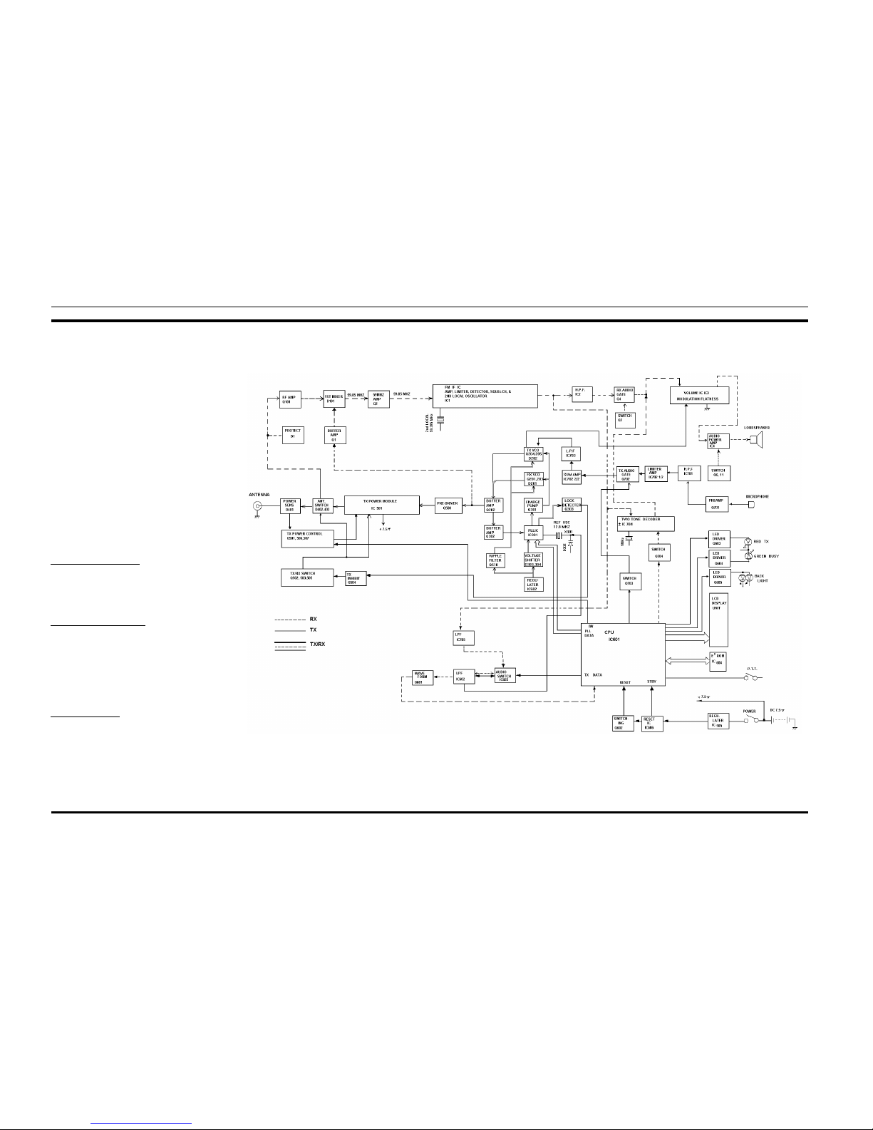
Figure 1 - Radio Block Diagram
RECEIVER
The receiver converts the received RF signal to an audio sig-
nal. The receiver contains the following:
• Antenna switch
• First RF amplifier
• First IF mixer
• First IF pre-amplifier
• IF IC
• De-emphasis
• Highpass filter
• Audio muting
• Volume controller
• Audio power amplifier
• Squelch control
The receiver is a double-conversion type with intermediate
frequencies of 59.85 MHz and 455 kHz. The receiver frequency
range is from 146 to 174 MHz and the bandwid th, without
alignment, is 28 MHz (VHF) or 438 to 470 MHz and the bandwidth, without alignment, is 32 MHz (UHF). The filters in the
receive section perform the receiver characteristics such as selectivity, image and spurious rejection and reduction of other
undesirable frequencies.
Antenna Switch (FT401)
The antenna switch in the receive mode permits RF signal to
pass to the receiver. In the transmit mode the circuit switches of f
the receiver and allows the RF signal from the transmitter to
feed the antenna through the transmit harmonic filter.
First RF Amplifier (Q101)
The antenna switch sends the received signal to Q101
through the bandpass filter. The received signal is filtered to reduce undesired frequenc i es ou t s ide the frequency band.
Q101 amplifies the filtered signal to recover the losses of
the antenna switch and the filters and to increase sensitivity.
Then this amplified signal is sent to the receive mixer through a
bandpass filter.
First MIxer (D101)
The received channel frequency is mixed with the first local
oscillator frequency to produce the first IF frequency (59.85
MHz). The first IF signal is sent through the 59.85 MHz crystal
bandpass filters (FT1 and FT2) to reduce adjacent channel undesired frequencies.
AE/LZB 119 1658 R1A
3

First IF Pre-Amplifier (Q2)
The filtered IF signal is applied to the first IF pre-amplifier Q2 to recover the losses of the filters and increase the
sensitivity of the received signal. Then it is sent to pin 24 of
the IF IC.
IF IC (IC1)
IC1 is a bipolar monolithic integrated circuit that provides all the functions of a comprehensive FM IF system.
This IC contains a second local oscillator, second IF mixer,
second IF amplifier, second IF limiting amplifier and a quadrature FM detector.
The second mixer combines the first IF signal with the
second local frequency (59.395 MHz) to produce the second
IF signal at 455 kHz.
The second IF signal is supplied to 455 kHz ceramic filters FT3 and FT4 to reduce noise near the second IF. The
signal is then applied to the second IF amplifier and limiting
amplifier. The limiting amplifier limits the signal to a specific level, removing any amplitude noise by clipping the
455 kHz signal. The limited 455 kHz signal is fed to the
quadrature detector and releases a demodulated audio signal
at pin 15 of IC1. This signal contains CTCSS tone (or
DCSS) and voice audio, or just a white noise at no rf signal
input.
De-Emphasis/Highpass Filter (R21, C33 And
IC2)
The output audio signal (with sub-audible data) at pin 15
of IF IC goes through de-emphasis cirucit (R21 and C33)
and highpass filter IC2. The de-emphasis circuit performs a
specific audio frequency response. The highpass filter attenuates the low frequency signal of CTCSS (or DCSS) contained in the demodulated signal.
RX Audio Muting (Q4 And Q7)
The audio output signal from the highpass filter is sent to
the audio frequency muting circuit Q4. The microprocessor
(pin 47) sends a mute control signal to Q4 through inverter
Q7.
The audio signal passes through the mute circuit when
the microprocessor sends a logical low level signal to the
mute circuit.
Volume Controller (IC3)
The audio signal is sent to the volume controller (pin 4 of
IC3). The microprocessor provides serial data to IC3 such as
clock, data and enable signals to control the audio output
level to the audio amplifier. Another volume controller (pin
14 of IC3) is connected to R218 of the transmit VCO and
controls the modulation flatness by the microprocessor.
The microprocessor (pin 10) generates a tone to indicate
radio conditions such as channel busy lockout, time out
timer and switch tone. This tone is applied to the volume
controller.
Audio Amplif ier ( IC4)
Pin 9 of IC4 receives and amplifies the audio signal from
the volume controller (pin 6 of IC3). Audio power output delivered to the internal speaker is normally more than 0.5
watts at 4 ohms. Pin 3 of IC4 releases the amplitude received
audio and sends it to the external speaker jack J3 then applies it to the internal speaker.
Squelch Circuit (IC1)
The IF IC also has a noise amplifier for squelch controller. RT1 adjust the input level of noise from the output of the
discriminator to set the squelch threshold level. Pin 19 of
IC1 sends the squelch signal to pin 56 of the microprocessor.
If the radio received a carrier, pin 19 of IC1 sends a logical low signal to the microprocessor.
TRANSMITTER
The transmitter converts an audio message to an RF signal and amplifies the RF signal to 5 watts at the antenna terminal. The transmitter frequency range is 146 to 174 MHz
and the bandwidth without alignment is 28 MHz (VHF) or
438 to 470 MHz and the bandwidth, without alignment, is
32 MHz (UHF). The transmitter contains the following circuits:
• Microphone amplifier
• Pre-emph asis and limiter
• Low pass filter
• Modulation buffer
• Pre-amplifier
• FM modulator
• Pre-driver
• RF power amplifier
• RF power controller
• Transmit inhibit
• Antenna switch
When the PTT switch is pressed, the negative side of the
microphone is grounded and DC bias voltage is applied to the
internal microphone to activate it. The microprocessor (pin 6)
detects the pressed PTT switch and switches Tx/Rx control
(pin 52) to the Tx mode (a logical low).
Microphone Amplifier (Q701)
The speech audio from the microphone enters the base of
Q701 and is amplified. Then it is released to the high pass filter
(IC701).
High Pass Filter/Pre-Emphasis /Limi ter Ampl ifier
The output signal of the microphone amplifier enters the
pre-emphasis/pre-amplifier (C703, Q701). The high pass filter
(IC701) removes any components in the sub-audible range (below 300 Hz) that would interfere with the CTCSS or DCSS
tone.
The output signal of the high pass filter enters the pre-emphasis/limiter amplifier (IC702) to provide limiting modulation.
MIC Mute (Q702 And Q703)
The output of the limiter is sent to the microphone mute
circuit Q702. The microprocessor (pin 48) sends a mute control signal to Q702 through an inverter Q703.
The audio signal passes through the mute circuit when the
microprocessor sends a logical low level to the mute circuit.
Low Pass Filter (IC703)
The limiter output is supplied to the low pass filter IC703
through a sum-amplifier IC702. The limiter output contains
high frequencies above 3 kHz. The low pass filter filters in
these high frequencies and releases them to pin 1 of IC703 and
then to the synthesizer.
TX Pre-Amplifier (Q508)
The output of the synthesizer is supplied to the pre-amplifier Q508. The Tx pre-amplifier increases the transmit signal to
a level sufficient to drive the power module.
Power Module And Power Controller (IC501,
L401, D401, Q501, Q506 And Q507)
The power amplifier circuit amplifies the output of the synthesizer to the proper output wattage (normally 5 watts at the
antenna connector). The transmit power detect circuit (L401
and D401) is connected to the output of the antenna switch
(D403) and monitors the transmit power.
The power control circuitry is a closed negative feedback
loop system (IC501, D401, Q501, Q506, Q507, IC501). It
monitors the transmit power and increases the control current
to the power module (pin 3 of IC501). If the RF output power
decreases, the transmit power is stabilized to the level adjusted
by RT501.
In the low power transmission, the microprocessor (pin 9 of
IC601) sends a logical low signal to the power control circuit
(base of Q501 through R513). The threshold level of the transmit power controller changes to the low power level. The
power amplifier circuit amplifies the output of the synthesizer
and the transmit local oscillator to the proper output wattage
(normally 1 watt at the antenna connector).
Transmit In hi bi t (Q502 An d Q503)
While the PLL is out of lock, pin 7 of PLL IC301 releases a
logical low to the transmit inhibit circuit Q503 through inverters Q303 and Q504. Since the output of Q503 turns Q502
off, no DC power is applied to the first stage of the power amplifier and the power controller to prevent transmission on an
improper frequency.
When the PLL is locked, pin 7 of IC301 becomes logical
high. This signal is supplied to Q503. The base of Q503 is
pulled to the transmit 5V line. The output of Q503 forces the
base of Q502 to ground; then the DC power is supplied to the
first stage of the power amplifier.
Antenna Switch (D402 And D403)
In the transmit mode, D402 and D403 receive the voltage,
transmit battery (7.5V). The circuit switches off the receiver
and allows RF signals to flow from the transmitter to the antenna, passing through the transmit harmonic filter that reduces
second and third harmonic frequencies generated within t he RF
amplifier.
AE/LZB 119 1658 R1A
4
REGULATORS
Transistor Q507 and the power module (pin 6 of IC501) are
directly connected to the battery through a fuse F1. When the
power switch of the radio is turned off, the current drain is almost zero.
When the power switch of the radio is turned ON, IC605
supplies 5.6V to most of the sections and IC502 supplies 5.6V
to the VCO and synthesizer section.
In the receive mode, pin 11 of the micropro ce ssor releases a
logical low level and turns transistor Q5 on. Q5 supplies 5.6V
to the receiver section.
In the transmit mode, pin 51 of the microprocessor releases
a logical low level and turns transistor Q505 on. Q505 supplies
5.6V to the transmitter section.
Components F1, D3, D4 and C50 reduce the damage to
other parts in the radio should a short circuit occur within the
radio or the polarity of the DC voltage is reversed.
LOGIC SECTION
The logic section contains the following:
• Microprocessor
• EEPROM memory
• Rx Tone Decoder
• 2-Tone Decoder
• Tx Tone Encoder
• Tone Generator
• Memory Back-up
• Reset Circuit
Microprocessor (IC601)
The microprocessor controls many of the transmit and receive functions. The microprocessor operates according to the
software instructions stored in the internal Read Only Memory
(ROM).
EEPROM (IC604)
The Electrically Erasable Programmable Read Only Memory (EEPROM) can be reprogrammed through the external microphone and speaker jacks J2 and J3.
IC604 stores the customer parameters such as channel information and function parameter. Since this device is a non-
volatile memory, IC604 retains all information in the
EEPROM even when po wer is removed.
The programming adapter is connected to the external microphone and speaker jacks J2 and J3. When the external
speaker output J3 is set to a logical high for a few seconds
from the programming adapter, that signal passes to pin 55 of
IC601 through R37 and D2. The radio enters into external programming mode. During programming, several commands and
data are exchanged throug h J2 between pins 19 and 20 of the
microprocessor.
The microprocessor sends serial data to the EEPROM
IC604 to store custormer data such as clock (pin 14), data (pin
13) and ROM enable (pin 50).
Receive T one Decoder (IC705, IC602 And Q601)
This circuit contains switched capacitor low pass filter
IC602 that is used in both transmit and receive modes. IC603
switches IC602 to function as either receive tone filter or transmit tone filter. The two op-amps in IC602 are comparators to
convert the analog waveform to digital waveform.
In the receive mode, the Tx/Rx control (pin 51 of IC601)
supplies a logical high signal to pins 5 and 6 of IC603. The
analog switches (pins 3 and 4, 8 and 9) in IC603 turn on. The
receive tone from the IF IC (pin 15 of IC1) is supplied to the
band pass filter IC705 through the gate of IC603 (pins 3 and
4).
When the radio receives DCSS data, the microprocessor
(pin 18 of IC601) sends a logical high to pin 13 of IC603. The
gate of IC603 (pins 1 and 2) turns on. The received DCSS code
is sent to the low pass filter (pin 8 of IC602).
Clock pulses from the microprocessor (pin 12) are applied
to pin 10 of IC705 and pin 9 of IC602, providing the cut-off
frequency of the filter as f
c
= f
clk
x 50.
The output signal of IC705 enters the low pass filter (pin 8
of IC602). The low pass filter only passes the desired tone and
filters out high frequencies contained in the receive data signal.
Filtered data is applied to pin 3 of IC602 and supplied to
op-amp #1 (pin 13 of IC602) through the gate of IC603 (pins 8
and 9). In this op-amp, receive data is amplified to approximately 1.2 Vp-p of level at pin 14 of IC602 (ad justed by
RT601). The amplified data is supplied t o a co mp arator (pin 14
of IC602, op-amp #2).
When the voltage at pin 14 of IC602 becomes greater than
that at pin 1, a logical low is released at pin 2 of IC602. When
the voltage at pi n 14 of IC602 decrea ses lower than pin 1, a
logical high is released at pin 2 of IC602. Voltage at pin 1 of
IC602 provides a reference level of the comparator around
the center of the data waveform.
Digitized data (square wave) is released at pin 2 of I C602
and applied to the microprocessor (pin 16) for decoding.
2-Tone Decoder
The received signal is also sent to the 2-tone decoder (pin
13 of IC704). The microprocessor provides serial data to
IC704 such as clock, data and enable signals to set tone information. The result of IC704 i s se nt to pi n 38 of IC601.
Transmit CTCSS Tone Or DCSS Encoder
(IC602)
In the transmit mode, the microprocessor sets the Tx/Rx
control (pin 52) to a logical low to turn Q505 on. The Tx 5V
is sent to pin 12 of IC603. The analog switch (pins 10 and
11) in IC603 turns on. The transmit tone or DCSS square
wave signal from the microprocessor (pin 17 of IC1) is supplied to the low pass filter (pin 8 of IC602) through the gate
of IC603 (pins 10 and 11).
Clock pulses from the microprocessor (pin 12) are applied to pin 9 of IC602, providing cut-off frequency of the
low pass filter the same as the decoder.
Filtered CTCSS tones or DCSS signals (pin 3 of IC602)
are applied to the sum-amplifier (pin 6 of IC702) through
RT701 (adjusts transmit deviation of the tone).
Tone Generator (IC601)
The microprocessor generates beep tone at pin 10 and
alerts the user of certain conditions in the radio. The generated tone is supplied to the volume controller (pin 4 of IC3)
to monitor from the speaker and and transmit sum-amplifier
(pin 6 of IC702) to modulate.
Memory Back-Up
Regulator IC605 supplies voltage to pins 72 aand 73 of
the microprocessor through D601. It also charges C618
through R616.
The microprocessor retains in Random Access Memory
(RAM) selected channel, deleted channels and scan status
while the power switch is turned off.
When the microprocessor senses that power is turned off
(pin 21 of IC601 goes low), the current drain into the microprocessor is decreased to save battery power, while the
power is turned off (standby mode).
When the power switch is off, the stored charged in
C618 keeps the microprocessor "alive" during the standby
mode.
Reset Circuitry
IC606 contains a Schmitt-Trigger circuit that maintains
the output voltage at appro ximately 0.7 V until the input
voltage reaches approximately 4.25V. When the input voltage exceeds 4.15V, IC606 releases an output voltage of the
same level after a del ay of approximately 200 microseconds.
When the output voltage of IC606 is high, a positive rising pulse is supplied to Q602 through C613. Q602 then releases a short duration, low pulse that is sent to pin 25 of
IC601. The microprocessor resets and normal operation begins.
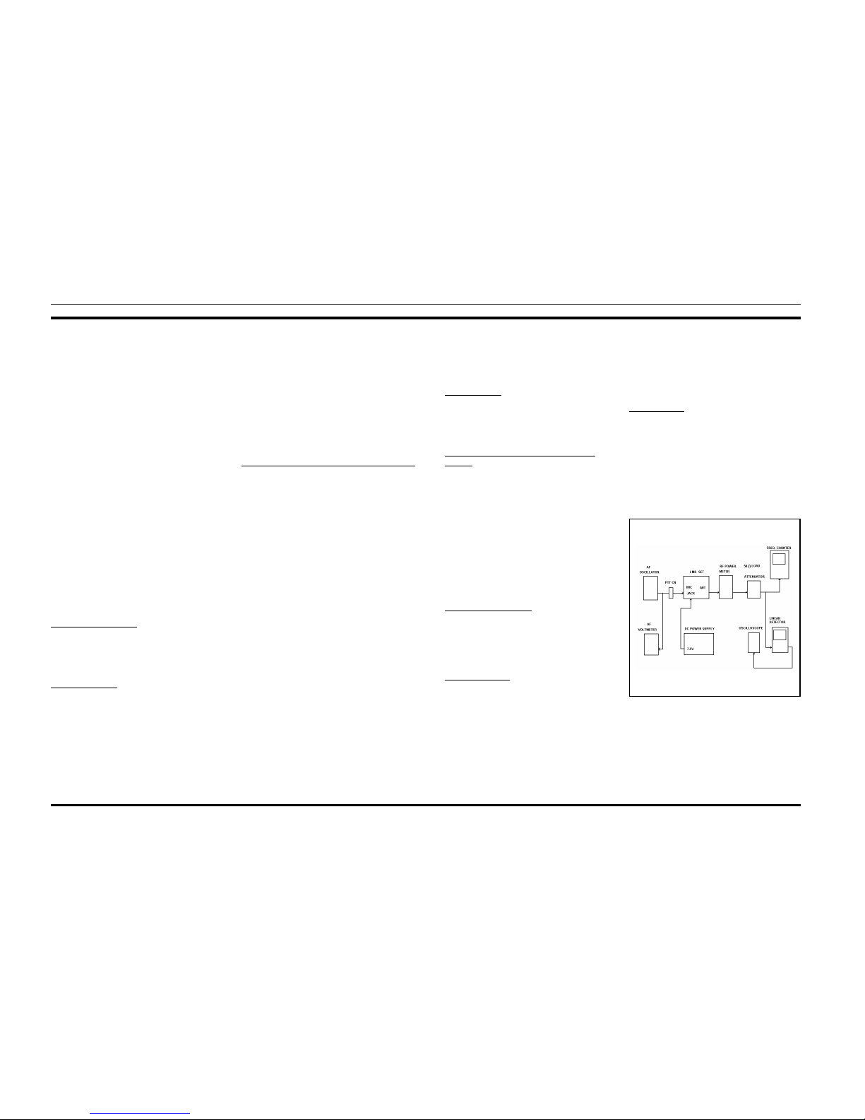
Figure 2 - Test Setup, Transmitter
AE/LZB 119 1658 R1A
5

VHF ALIGNMENT
ALIGNMENT OF TRANSMITTER - VHF
TEST EQUIPMENT REQUIRED
a. DC POWER SUPPLY (7.5V, more than 3A)
b. RF WATTMETER (more than 1 0 Watt)
c. DUMMY LOAD FOR SPEAKER (50 Ω more than 10 Watt)
d. FM LINEAR DETECTOR
e. FREQUENCY COUNTER
f. AF OSCILLATOR
ALIGNMENT CONDITION
a. CHANNEL : 1
b. MODE : TX
c. MODULATION FREQUENCY : 1 kHz
d. LOAD IMPEDANCE : 50 Ω
ALIGNMENT PROCEDURE
See Figure 2 for setup of test equ i pm en t .
STEP TEST CONDITION MEASUREMENT ADJUSTMENT REMARKS
1
NO MODULATION
RF W ATTMETE R RT501 4.8 W ± 0.05 W *
2 FREQUENCY
COUNTER
CT301 161.000 MHz ± 100 Hz
3
MOD : 1 kHz
LEVEL : 100 mV
FM LINEAR
DETECTOR
HPF: OFF
LPF: OFF
DE-EMPHASIS: OFF
RT20 2 ± 4.0 kHz DEV ± 0.01 kHz
4CH6
NO MODULATION
↑
RT70 1 ± 700 Hz DEV ± 10 Hz
(Tone Freq. = 67.0 Hz)
5CH7
↑
RT20 1 ± 700 Hz DEV ± 10 Hz
(Tone Freq. = 250.3 Hz)
6CH6
↑
--------- If DEVIATION is not ± 700 Hz
DEV ± 30 Hz back to STEP 5.
7CH1
MOD : 1 kHz, 100 mV
↑
RT20 2
(CHECK)
± 4.0 kHz DEV ± 0.05 kHz
8CH4
NO MODULATION
↑
RT70 1
(CHECK)
± 700 Hz DEV ± 30 Hz
(Tone Freq. = 167.9 Hz)
*
POWER ADJUSTMENT TIME IS LESS THAN 5 SE CONDS.
ALIGNMENT OF RECEIVER - VHF
TEST EQUIPMENT REQUIRED
a. DC POWER SUPPLY (7.5V, MORE THAN 2A)
b. RF SIGNAL GENERATOR
c. DUMMY LOAD FOR SPEAKER (8 Ω, more than 1 Watt)
d. SINAD METER
e. AF OSCILLATOR
f. OSCILLOSCOPE
ALIGNMENT CONDITION
a. CHANNEL : 2
b. MODE : RX
c. SQUELCH (RT001 : SW. VR) : C.C.W.
d. RF SSG MODULATION : 1 kHz, ± 3 kHz DEV.
e. RF SSG FREQUENCY : 146.05 MHz
f. AUDIO SIGNAL OUTPUT LEVEL : 50 mW (0.63 Vrms)
(AT SPEAKER TERMINAL)
ALIGNMENT PROCEDURE
See Figure 3 for setup of test equ i pm en t .
STEP TEST CONDITION MEASUREMENT ADJUSTMENT REMARKS
1
RF SSG
LEVEL :0.10 uV
OSCILLOSCOPE
(AUDIO OUTPUT)
RT001 ADJUST RT001 TO THE POINT
WHERE AUDIO OUTPUT WAVEFORM WILL APPEAR
2
CHANNEL: 4
RF SSG
LEVEL: 1 mV
MOD: 167.90 Hz
DEV: ± 700 Hz
TP601 RT601 ADJUST RT6 01 TO
0.9Vp-p
0.9Vp-p
*RED LED FLASHING DURING
ADJUST
AE/LZB 119 1658 R1A
6
VHF ALIGNMENT
Figure 3 - Test Setup, Receiver
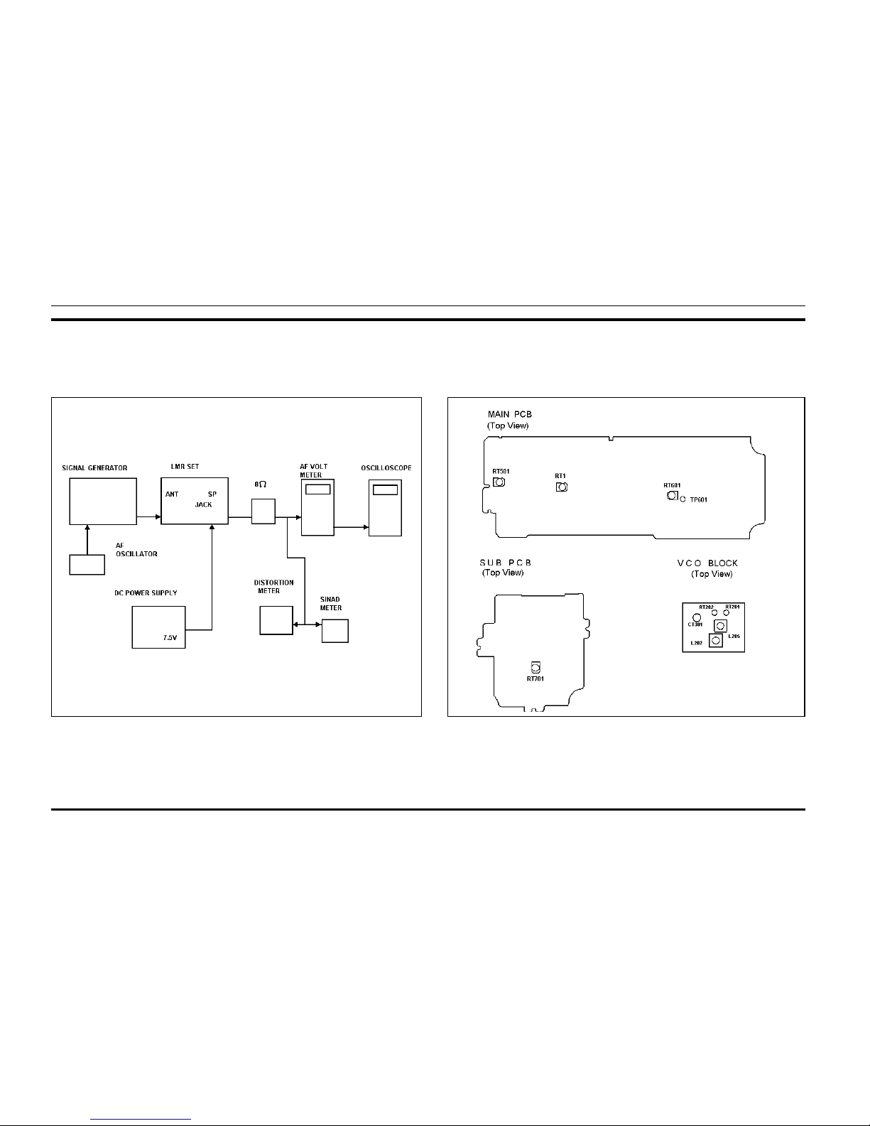
Figure 4 - Alignment Points, VHF
ALIGNMENT PROCEDURE
AE/LZB 119 1658 R1A
7
VHF
TEST MODE (VHF)
DETAIL OF TEST MODE ROM
CH
RX TX
2-TONE VOX USES
FREQ.
(MHz)
CTCSS/DCS
(Hz) (-)
FREQ.
(MHz)
CTCSS/DCS
(Hz) (-)PW
R
1 160.0500 - - - - - - - - - - - - - 161.0000 - - - - - - - - - - - --HI - - - - - - - OFF ALIGNMENT OF TX/RX
2 146.0500 - - - - - - - - - - - - - 146.5000 - - - - - - - - - - - --HI - - - - - - - OFF ALIGNMENT OF TX/RX
3 173.9500 - - - - - - - - - - - - - 173.5000 - - - - - - - - - - - --HI - - - - - - - OFF ALIGNMENT OF TX/RX
4 160.0500 CTCSS 167.9 161.0000 CTCSS 167.9 HI - - - - - - - OFF ALIGNMENT OF CTCSS
5 160.0500 DCS CODE 172 161.0000 DCS CODE 172 HI - - - - - - - OFF ALIGNMENT OF DCS
6 160.0500 CTCSS 67.0 161.0000 CTCSS 67.0 HI - - - - - - - OFF ALIGNMENT OF CTCSS
7 160.0500 CTCSS 250.3 161.0000 CTCSS 250.3 HI - - - - - - - OFF ALIGNMENT OF CTCSS
8 160.0500 - - - - - - - - - - - - - 161.0000 - - - - - - - - - - - --LO 288.5
1433.4
ON CONFIRM OF 2-TONE
TX LOW
9 146.0500 - - - - - - - - - - - - - 146.5000 - - - - - - - - - - - --LO - - - - - - - ON TX LOW
10 173.9500 - - - - - - - - - - - - - 173.5000 - - - - - - - - - - - --LO - - - - - - - ON TX LOW
11 146.0500 CTCSS 67.0 146.5000 CTCSS 67.0 HI - - - - - - - OFF - - - - - - - - - - - - 12 146.0500 CTCSS 250.3 146.5000 CTCSS 250.3 HI - - - - - - - OFF - - - - - - - - - - - - 13 173.9500 CTCSS 67.0 173.5000 CTCSS 67.0 HI - - - - - - - OFF - - - - - - - - - - - - 14 173.9500 CTCSS 250.3 173.5000 CTCSS 250.3 HI - - - - - - - OFF - - - - - - - - - - - - 15 150.0500 CTCSS 67.0 150.0500 CTCSS 67.0 HI - - - - - - - OFF FIELD TEST
16 150.5000 CTCSS 250.3 150. 5000 CTCSS 250.3 HI - - - - - - - OFF FIELD TEST
PC PROGRAMMING
TIME OUT TIMER OFF
PRIORITY CHANNEL CH 1
DROP OUT DELAY 1 SEC
SCAN ON
BUSY CHANNEL LOCKOUT OFF
TRANSISTOR
VOLTAGE CHART (VHF)
Q
PIN NO.
RX
[V]TX[V]
REMARKS
Q001 C 5.0 0.0
B0.70.0
E0.00.0
Q002 C 1.0 0.0
B0.70.0
E0.00.0
Q004 S 2.8 0.6
G0.00.0
D0.90.6
Q005 C 5.5 0.0
B4.95.6
E5.65.6
Q006 C 0.9 0.9
B7.57.1
E7.57.2
Q007 C 0.0 0.0
B5.05.0
E0.00.0
Q011 C 7.5 7.1
B0.00.0
E0.00.0
Q501 C1 0.0 0.6
C2 0.0 0.0
B1 0.0 4.5
B2 0.0 4.5
E0.05.0
Q502 C 0.0 7.2
B7.56.4
E7.57.2
Q503 C 7.5 6.4
B0.04.6
E0.03.9
Q504 C 0.0 4.6
B0.00.0
E0.00.0
Q505 C 0.0 5.6
B5.55.0
E5.65.6
Q506 C 7.0 6.4
B0.00.6
E0.00.0
Q
PIN NO.
RX
[V]TX[V]
REMARKS
Q507 C 0.0 3.0
B7.06.6
E7.57.2
Q508 C 0.0 4.9
B0.00.7
E0.00.0
Q510 C 5.6 5.6
B5.55.5
E4.84.8
Q601 C1 0.0 0.0
C2 5.2 5.2
B1 2.3 2.6
B2 2.3 2.6
E2.32.6
Q602 C 5.0 5.0
B0.00.0
E0.00.0
Q603 C 7.5 7.5
B0.00.0
E0.00.0
Q604 C 7.5 7.5
B0.00.0
E0.00.0
Q605 C 7.5 7.5
B0.00.0
E0.00.0
Q701 C 1.6 1.6
B0.70.7
E0.10.1
Q702 S 3.2 3.2
G0.00.0
D3.23.2
Q704 C 1.8 1.8
B5.25.2
E5.65.6
AE/LZB 119 1658 R1A
8

VHF
VOLTAGE CHART - (VHF)
IC001
PIN NO.
RX
[V]TX[V]
REMARKS
15.40.0
24.70.0
35.50.0
44.20.0
55.50.0
65.00.0
75.00.0
84.40.0
95.50.0
10 5.5 0.0
11 5.1 0.0
12 0.0 0.0
13 4.6 0.0
14 5.5 0.0
15 0.9 0.0
16 1.0 0.0
17 0.7 0.0
18 0.7 0.0
19 5.4 0.0
20 NC 0.0
21 0.2 0.0
22 5.5 0.0
23 0.0 0.0
24 1.0 0.0
IC002
PIN NO.
RX
[V]TX[V]
REMARKS
13.00.6
23.00.4
33.00.2
40.00.0
53.00.2
63.00.6
72.80.6
85.60.6
IC003
PIN NO.
RX
[V]TX[V]
REMARKS
10.00.0
2NCNC
3NCNC
40.00.0
50.00.0
60.00.0
7NCNC
80.00.0
90.00.0
10 0.0 0.0
11 0.0 0.0
12 NC NC
13 NC NC
14 0.0 0.0
15 0.0 0.0
16 0.0 0.0
17 NC NC
18 NC NC
19 NC NC
20 5.6 5.6
IC004
PIN NO.
RX
[V]TX[V]
REMARKS
10.90.9
20.00.0
30.60.6
40.00.0
50.80.8
60.80.8
70.00.0
80.60.6
90.00.0
IC501
PIN NO.
RX
[V]TX[V]
REMARKS
1 0.0 1.2 INPUT
2 0.0 7.3 Vs1
3 0.0 3.6 Vcontrol
4 0.0 7.3 Vs2
5 7.5 7.5 Vs3
6 0.0 0.0 OUTPUT
VOLTAGE CHART - (VHF)
IC502
PIN NO.
RX
[V]TX[V]
REMARKS
10.00.0
27.57.2
35.65.6
IC502
PIN NO.
RX
[V]TX[V]
REMARKS
12.32.6
2 - - - - DATA LINE
32.12.3
42.32.6
52.32.6
65.25.2
72.32.6
82.32.6
9 - - - - CLOCK LINE
10 0.0 0.0
11 NC NC
12 0.0 0.0
13 2.3 2.6
14 2.3 2.6
IC603
PIN NO.
RX
[V]TX[V]
REMARKS
12.32.6
22.32.5
32.32.5
42.32.3
55.00.0
65.00.0
70.00.0
82.12.3
92.12.4
10 2.3 2.6
11 1.6 2.6
12 0.0 5.6
13 0.0 5.0
14 5.2 5.2
IC604
PIN NO.
RX
[V]TX[V]
REMARKS
10.00.0
2 - - - - CLOCK LINE
3 - - - - DATA LINE
4 - - - - COMMON PIN3
50.00.0
6NCNC
7NCNC
85.25.2
IC605
PIN NO.
RX
[V]TX[V]
REMARKS
10.00.0
27.57.2
35.65.6
IC606
PIN NO.
RX
[V]TX[V]
REMARKS
15.25.2
20.00.0
35.15.1
IC701
PIN NO.
RX
[V]TX[V]
REMARKS
13.23.2
23.23.2
33.13.1
40.00.0
53.13.1
63.23.2
73.23.2
85.65.6
IC702
PIN NO.
RX
[V]TX[V]
REMARKS
13.23.2
23.23.2
33.23.2
40.00.0
53.23.2
63.23.2
73.23.2
85.65.6
AE/LZB 119 1658 R1A
9
VHF
VOLTAGE CHART - (VHF)
IC703
PIN NO.
RX
[V]TX[V]
REMARKS
13.23.2
23.23.2
33.13.1
40.00.0
53.13.1
63.23.2
73.13.1
85.65.6
PCB:SWITCH
PIN NAME
RX
[V]TX[V]
REMARKS
GND 0.0 0.0
DET 0.0 4.6 ADJUSTABLE
GND 0.0 0.0
RX 0.0 0.8
TX7.5V 0.0 7.2
GND 0.0 0.0
TX 0.0 0.0
PCB:RF
PIN NAME
RX
[V]TX[V]
REMARKS
GND 0.0 0.0
IN 0.0 0.0
GND 0.0 0.0
RX5.6V 5.5 0.0
LOCAL 0.0 0.0
GND 0.0 0.0
IF OUT 0.0 0.0
GND 0.0 0.0
PCB:RF
PIN NAME
RX
[V]TX[V]
REMARKS
OUT 0.0 0.0
GND 0.0 0.0
GND 0.0 0.0
MOD 0.0 0.0
BAL - - - - NOT ON
MAIN PCB
UNLOCK 0.0 0.0
CLOCK - - - - CLOCK LINE
DATA - - - - DATA LINE
PLL_EN 0.3 0.3
5V 5.0 5.0
Tx5 0.0 5.6
Rx5 5.5 0.0
VCO5 4.8 4.8
REF
NO.
POLARITY RX
[V]TX[V]
REMARKS
C23 + 5.5 0.0
C37 + 3.0 0.6
C53 + 0.0 0.0
C54 +
−
0.6
0.0
0.6
0.0
C55 + 9.0 0.9
C63 + 0.6 0.6
C64 + 0.8 0.8
C65 +
−
0.8
0.6
0.8
0.6
C507 + 0.0 0.6
C515 + 0.0 7.1
C530 + 5.5 5.5
C532 + 5.6 5.6
C602 + 7.5 7.2
C603 + 5.6 5.6
C608 + 2.3 2.6
C610 + 2.3 2.6
C618 + 5.1 5.1
C619 + 5.2 5.2
C623 + 5.2 5.2
C633 + 5.2 5.2
C702 + 5.2 5.2
C707 + 4.4 4.4
C716 + 3.3 3.3
C717 + 3.2 3.2
C718 +
−
3.2
3.2
3.2
3.2
C729 +
−
3.3
2.3
3.3
2.3
C731 +
−
3.1
0.0
3.1
0.0
C732 +
−
3.3
2.0
3.3
2.3
C738 + 7.5 7.4
C752 + 1.8 1.8
C755 + 0.9 0.9
C758 + 5.6 5.6
C765 + 5.6 5.6
C768 + 3.0 3.0
VOLTAGE CHART - (VHF)
AE/LZB 119 1658 R1A
10
UHF ALIGNMENT
ALIGNMENT OF TRANSMITTER - (UHF)
TEST EQUIPMENT REQUIRED
a. DC POWER SUPPLY (7.5V, more than 3A)
b. RF WATTMETER (more than 1 0 Watt)
c. DUMMY LOAD FOR SPEAKER (50 Ω more than 10 Watt)
d. FM LINEAR DETECTOR
e. FREQUENCY COUNTER
f. AF OSCILLATOR
ALIGNMENT CONDITION
a. CHANNEL : 1
b. MODE : TX
c. MODULATION FREQUENCY : 1 kHz
d. LOAD IMPEDANCE : 50 Ω
ALIGNMENT PROCEDURE
See Figure 2 for setup of test equ i pm en t .
STEP TEST CONDITION MEASUREMENT ADJUSTMENT REMARKS
1
NO MODULATION
RF W ATTMETER RT501 3.8W ± 0.05W *
2 FREQUENCY
COUNTER
CT301 461.000 MHz ± 100 Hz
3
MOD : 1 kHz
LEVEL : 100 mV
FM LINEAR
DETECTOR
HPF: OFF
LPF: OFF
DE-EMPHASIS: OFF
RT20 2 ± 4.0 kHz DEV ± 0.01 kHz
4CH6
NO MODULATION
↑
RT70 1 ± 700 Hz DEV ± 10 Hz
(Tone Freq. = 67.0 Hz)
5CH7
↑
RT20 1 ± 700 Hz DEV ± 10 Hz
(Tone Freq. = 250.3 Hz)
6CH6
↑
--------- If DEVIATION is not ± 700 Hz DEV
± 30 Hz back to STEP 5.
7CH1
MOD : 1 kHz, 100 mV
↑
RT20 2
(CHECK)
± 4.0 kHz DEV ± 0.05 kHz
8CH4
NO MODULATION
↑
RT70 1
(CHECK)
± 700 Hz DEV ± 30 Hz
(Tone Freq. = 167.9 Hz)
*
POWER ADJUSTMENT TIME IS LESS THAN 5 SE CONDS.
ALIGNMENT OF RECEIVER - (UHF)
TEST EQUIPMENT REQUIRED
a. DC POWER SUPPLY (7.5V, more than 2A)
b. RF SIGNAL GENERATOR
c. DUMMY LOAD FOR SPEAKER (8 Ω, more than 1 Watt)
d. SINAD METER
e. AF OSCILLATOR
ALIGNMENT CONDITION
a. CHANNEL : 2
b. MODE : RX
c. SQUELCH (RT001 : SQ. VR) : C.C.W.
d. RF SSG MODULATION : 1 kHz, ± 3 kHz DEV.
e. RF SSG FREQUENCY : 438.05 MHz
f. AUDIO SIGNAL OUTPUT LEVEL : 50 mW (0.63 Vrms)
(AT SPEAKER TERMINAL)
ALIGNMENT PROCEDURE
See Figure 3 for setup of test equ i pm en t .
STEP TEST CONDITION MEASUREMENT ADJUSTMENT REMARKS
1
RF SSG
LEVEL :0.15 uV
OSCILLOSCOPE
(AUDIO OUTPUT)
RT001 ADJUST RT001 TO THE POINT
WHERE AUDIO OUTPUT WAVEFORM WILL APPEAR
2
CHANNEL: 4
RF SSG
LEVEL: 1 mV
MOD: 167.90 Hz
DEV: ± 700 Hz
TP601 RT601 ADJUST RT6 01 TO
0.9Vp-p
0.9Vp-p
AE/LZB 119 1658 R1A
11

UHF ALIGNMENT
Figure 5 - Alignement Points, UHF
TEST MODE (UHF)
DETAIL OF TEST MODE ROM
CH
RX TX
2-TONE VOX USES
FREQ.
(MHz)
CTCSS/DCS
(Hz) (-)
FREQ.
(MHz)
CTCSS/DCS
(Hz) (-)
P
W
R
1 460.0500 - - - - - - - - - - - - - 461.0000 - - - - - - - - - - - - - HI - - - - - - - OFF ALIGNMENT OF TX/RX
2 438.0500 - - - - - - - - - - - - - 438.5000 - - - - - - - - - - - - - HI - - - - - - - OFF ALIGNMENT OF TX/RX
3 469.9500 - - - - - - - - - - - - - 469.5000 - - - - - - - - - - - - - HI - - - - - - - OFF ALIGNMENT OF TX/RX
4 460. 0500 CTCSS 167.9 461.0000 CTCSS 167.9 HI - - - - - - - OFF ALIGNMENT OF CTCSS
5 460.0500 DCS CODE 172 461.0000 DCS CODE 172 HI - - - - - - - OFF ALIGNMENT OF DCS
6 460.0500 CTCSS 67.0 461.0000 CTCSS 67.0 HI - - - - - - - OFF ALIGNMENT OF CTCSS
7 460.0500 CTCSS 250.3 461.0000 CTCSS 250.3 HI - - - - - - - OFF ALIGNMENT OF CTCSS
8 460.0500 - - - - - - - - - - - - - 461.0000 - - - - - - - - - - - - - LO 288.5
1433.4
ON CONFIRM OF 2-TONE
TX LOW
9 438. 0500 - - - - - - - - - - - - - 438.5000 - - - - - - - - - - - - - LO - - - - - - - ON TX LOW
10 469.9500 - - - - - - - - - - - - - 469.5000 - - - - - - - - - - - - - LO - - - - - - - ON TX LOW
11 438.0500 CTCSS 67.0 438.5000 CTCSS 67.0 HI - - - - - - - OFF - - - - - - - - - - - - 12 438.0500 CTCSS 250.3 438.5000 CTCSS 250.3 HI - - - - - - - OFF - - - - - - - - - - - - 13 469.9500 CTCSS 67.0 469.5000 CTCSS 67.0 HI - - - - - - - OFF - - - - - - - - - - - - 14 469.9500 CTCSS 250.3 469.5000 CTCSS 250.3 HI - - - - - - - OFF - - - - - - - - - - - - 15 450.0500 CTCSS 67.0 450.0500 CTCSS 67.0 HI - - - - - - - OFF FIELD TEST
16 450.5000 CTCSS 250.3 450.5000 CTCSS 250.3 HI - - - - - - - OFF FIELD TEST
PC PROGRAMMING
TIME OUT TIMER OFF
PRIORITY CHANNEL CH 1
DROP OUT DELAY 1 SEC
SCAN ON
BUSY CHANNEL LOCKOUT OFF
AE/LZB 119 1658 R1A
12

UHF
TRANSISTOR
VOLTAGE CHART (UHF)
Q
PIN NO.
RX
[V]TX[V]
REMARKS
Q001 C 5.0 0.0
B0.70.0
E0.00.0
Q002 C 1.0 0.0
B0.70.0
E0.00.0
Q004 S 2.8 0.6
G0.00.0
D0.90.6
Q005 C 5.5 0.0
B4.95.6
E5.65.6
Q006 C 0.9 0.9
B7.57.1
E7.57.2
Q007 C 0.0 0.0
B5.05.0
E0.00.0
Q011 C 7.5 7.1
B0.00.0
E0.00.0
Q501 C1 0.0 0.6
C2 0.0 0.0
B1 0.0 4.5
B2 0.0 4.5
E0.05.0
Q502 C 0.0 7.2
B7.56.4
E7.57.2
Q503 C 7.5 6.4
B0.04.6
E0.03.9
Q504 C 0.0 4.6
B0.00.0
E0.00.0
Q505 C 0.0 5.6
B5.55.0
E5.65.6
Q506 C 7.0 6.4
B0.00.6
E0.00.0
Q
PIN NO.
RX
[V]TX[V]
REMARKS
Q507 C 0.0 3.0
B7.06.6
E7.57.2
Q508 C 0.0 4.9
B0.00.7
E0.00.0
Q510 C 5.6 5.6
B5.55.5
E4.84.8
Q601 C1 0.0 0.0
C2 5.2 5.2
B1 2.3 2.6
B2 2.3 2.6
E2.32.6
Q602 C 5.0 5.0
B0.00.0
E0.00.0
Q603 C 7.5 7.5
B0.00.0
E0.00.0
Q604 C 7.5 7.5
B0.00.0
E0.00.0
Q605 C 7.5 7.5
B0.00.0
E0.00.0
Q701 C 1.6 1.6
B0.70.7
E0.10.1
Q702 S 3.2 3.2
G0.00.0
D3.23.2
Q704 C 1.8 1.8
B5.25.2
E5.65.6
VOLTAGE CHART - (UHF)
IC001
PIN NO.
RX
[V]TX[V]
REMARKS
15.40.0
24.70.0
35.50.0
44.20.0
55.50.0
65.00.0
75.00.0
84.40.0
95.50.0
10 5.5 0.0
11 5.1 0.0
12 0.0 0.0
13 4.6 0.0
14 5.5 0.0
15 0.9 0.0
16 1.0 0.0
17 0.7 0.0
18 0.7 0.0
19 5.4 0.0
20 NC 0.0
21 0.2 0.0
22 5.5 0.0
23 0.0 0.0
24 1.0 0.0
IC002
PIN NO.
RX
[V]TX[V]
REMARKS
13.00.6
23.00.4
33.00.2
40.00.0
53.00.2
63.00.6
72.80.6
85.65.6
IC003
PIN NO.
RX
[V]TX[V]
REMARKS
10.00.0
2NCNC
3NCNC
40.00.0
50.00.0
60.00.0
7NCNC
80.00.0
90.00.0
10 0.0 0.0
11 0.0 0.0
12 NC NC
13 NC NC
14 0.0 0.0
15 0.0 0.0
16 0.0 0.0
17 NC NC
18 NC NC
19 NC NC
20 5.6 5.6
IC004
PIN NO.
RX
[V]TX[V]
REMARKS
10.90.9
20.00.0
30.60.6
40.00.0
50.80.8
60.80.8
70.00.0
80.60.6
90.00.0
IC501
PIN NO.
RX
[V]TX[V]
REMARKS
10.02.4
20.07.1
30.03.0
40.07.1
57.57.2
67.57.2
70.00.0
AE/LZB 119 1658 R1A
13
UHF
VOLTAGE CHART - (UHF)
IC502
PIN NO.
RX
[V]TX[V]
REMARKS
10.00.0
27.57.2
35.65.6
IC502
PIN NO.
RX
[V]TX[V]
REMARKS
12.32.6
2 - - - - DATA LINE
32.12.3
42.32.6
52.32.6
65.25.2
72.32.6
82.32.6
9 - - - - CLOCK LINE
10 0.0 0.0
11 NC NC
12 0.0 0.0
13 2.3 2.6
14 2.3 2.6
IC603
PIN NO.
RX
[V]TX[V]
REMARKS
12.32.6
22.32.5
32.32.5
42.32.3
55.00.0
65.00.0
70.00.0
82.12.3
92.12.4
10 2.3 2.6
11 1.6 2.6
12 0.0 5.6
13 0.0 5.0
14 5.2 5.2
IC604
PIN NO.
RX
[V]TX[V]
REMARKS
10.00.0
2 - - - - CLOCK LINE
3 - - - - DATA LINE
4 - - - - COMMON PIN3
50.00.0
6NCNC
7NCNC
85.25.2
IC605
PIN NO.
RX
[V]TX[V]
REMARKS
10.00.0
27.57.2
35.65.6
IC606
PIN NO.
RX
[V]TX[V]
REMARKS
15.25.2
20.00.0
35.15.1
IC701
PIN NO.
RX
[V]TX[V]
REMARKS
13.23.2
23.23.2
33.13.1
40.00.0
53.13.1
63.23.2
73.23.2
85.65.6
IC702
PIN NO.
RX
[V]TX[V]
REMARKS
13.23.2
23.23.2
33.23.2
40.00.0
53.23.2
63.23.2
73.23.2
85.65.6
VOLTAGE CHART - (UHF)
REF
NO.
POLARITY RX
[V]TX[V]
REMARKS
C23 + 5.5 0.0
C37 + 3.0 0.6
C53 + 0.0 0.0
C54 +
−
0.6
0.0
0.6
0.0
C55 + 9.0 0.9
C63 + 0.6 0.6
C64 + 0.8 0.8
C65 +
−
0.8
0.6
0.8
0.6
C507 + 0.0 0.6
C515 + 0.0 7.1
C530 + 5.5 5.5
C532 + 5.6 5.6
C602 + 7.5 7.2
C603 + 5.6 5.6
C608 + 2.3 2.6
C610 + 2.3 2.6
C618 + 5.1 5.1
C619 + 5.2 5.2
C623 + 5.2 5.2
C633 + 5.2 5.2
C702 + 5.2 5.2
C707 + 4.4 4.4
C716 + 3.3 3.3
C717 + 3.2 3.2
C718 +
−
3.2
3.2
3.2
3.2
C729 +
−
3.3
2.3
3.3
2.3
C731 +
−
3.1
0.0
3.1
0.0
C732 +
−
3.3
2.0
3.3
2.3
C738 + 7.5 7.4
C752 + 1.8 1.8
C755 + 0.9 0.9
C758 + 5.6 5.6
C765 + 5.6 5.6
C768 + 3.0 3.0
IC703
PIN NO.
RX
[V]TX[V]
REMARKS
13.23.2
23.23.2
33.13.1
40.00.0
53.13.1
63.23.2
73.13.1
85.65.6
PCB:SWITCH
PIN NAME
RX
[V]TX[V]
REMARKS
GND 0.0 0.0
DET 0.0 4.6 ADJUSTABLE
GND 0.0 0.0
RX 0.0 0.8
TX7.5V 0.0 7.2
GND 0.0 0.0
TX 0.0 0.0
PCB:RF
PIN NAME
RX
[V]TX[V]
REMARKS
GND 0.0 0.0
IN 0.0 0.0
GND 0.0 0.0
RX5.6V 5.5 0.0
LOCAL 0.0 0.0
GND 0.0 0.0
IF OUT 0.0 0.0
GND 0.0 0.0
SYNTHE. UNIT
PIN NAME
RX
[V]TX[V]
REMARKS
OUT 0.0 0.0
GND 0.0 0.0
GND 0.0 0.0
MOD 0.0 0.0
BAL - - - - NOT ON
MAIN PCB
UNLOCK 0.0 0.0
CLOCK - - - - CLOCK LINE
DATA - - - - DATA LINE
PLL_EN 0.3 0.3
5V 5.0 5.0
Tx5 0.0 5.6
Rx5 5.5 0.0
VCO5 4.8 4.8
AE/LZB 119 1658 R1A
14
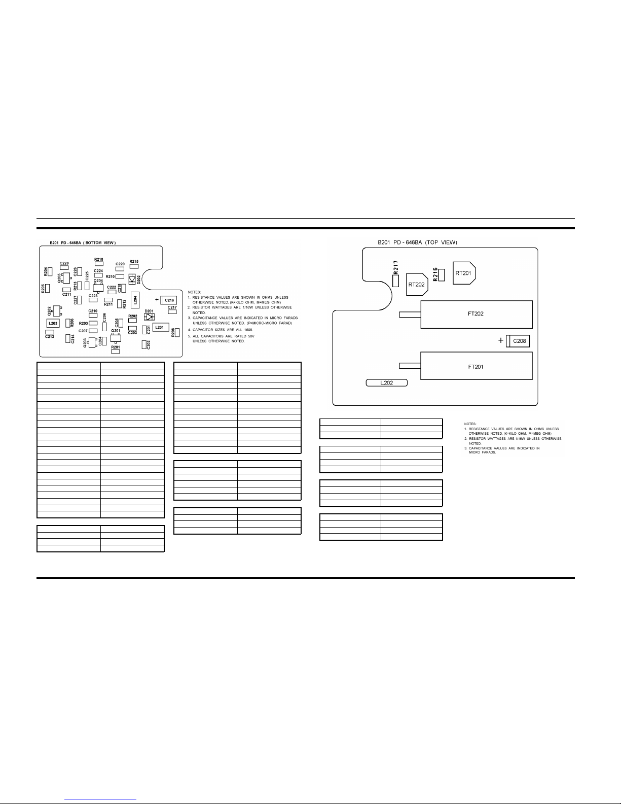
VCO BOARD (UHF)
TOP VIEW
(E24-12157, Sh. 1, Rev. 0)
ASSEMBLIES
C201 15P / CH
C202 3P / CJ
C203 3P / CJ
C204 0.001 / B
C205 10P / CH
C206 10P / CH
C207 0.001 / B
C210 2P / CK
C211 330P / CH
C213 330P / CH
C214 12P / CH
C216 35V0.1 (T) C-227
C217 330P / CH
C218 15P / CH
C220 330P / CH
C222 4P / CH
C223 0.001 / B
C224 12P / CH
C225 10P / CH
C226 0.001 / B
C227 2P / CK
C228 330P / CH
D201 HVU350
D202 HVU350
R201 3.9K
R202 4.7K
R203 330
R204 100
R205 220
R206 47K
R208 1K
R210 100
R211 3.9K
R212 4.7K
R213 330
R215 47K
R218 1K
Q201 2SC4226 - R24
Q202 2SC4226 - R24
Q203 DTC124XU
Q204 2SC4226 - R24
Q205 DTC124XU
L201 0.1uH LZ - 116
L203 0.018uH LZ - 087
L204 0.1uH LZ - 116
VCO BOARD (UHF)
BOTTOM VIEW
(E24-12155, Sh. 1, Rev. 1)
C208 7V10 (T) C - 241
R216 10K
R217 22K
RT201 47KB RT - 550
RT202 47KB RT - 550
FT201 FK - 049
FT202 FK - 049
L202 LE - 351 1/2T
AE/LZB 119 1658 R1A
15
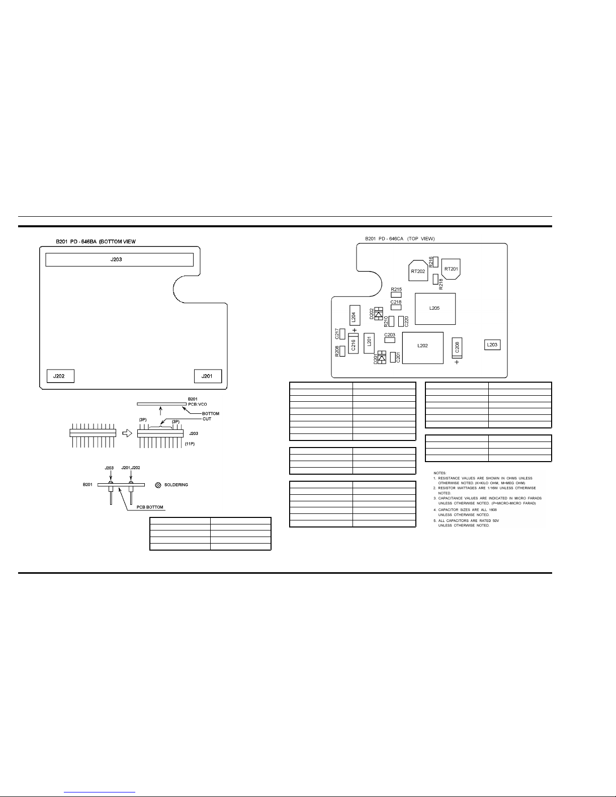
VCO BOARD (UHF)
BOTTOM VIEW
(E24-12154, Sh. 2, Rev. 0)
ASSEMBLIES
J201 PG - 156 2P
J202 PG - 156 2P
J203 PG - 156 11P
C201 18P / CH
C203 5P / CH
C208 7V10 (T) C - 241
C216 35V0.1 (T) C-227
C217 330P / CH
C218 100P / CH
C220 330P / CH
D201 MA376
D202 MA366
R208 1K
R210 100
R215 33K
R216 0
R218 5.6K
VCO BOARD (UHF)
TOP VIEW
(E24-12267, Rev. 1)
L201 0.75uH LZ - 140
L202 LF - 257
L203 0.068uH LZ - 087
L204 0.75uH LZ - 140
L205 LF - 258
RT201 47KB RT - 550
RT202 47KB RT - 550
AE/LZB 119 1658 R1A
16
 Loading...